International Journal of Scientific & Engineering Research Volume 2, Issue 3, March-2011 1
ISSN 2229-5518
Preparation, Verification and Finding Out of the Critical Current of Thin Sample of YBCO Compounds
Shaikh Md. Rubayiat Tousif, Shaiyek Md. Buland Taslim
Abstract— This paper is all about superconductors. It deals with the current state of high temperature superconductors (HTS), the application of these materials and possible breakthroughs in the field. It also provides information about how to synthesize YBCO compounds and explains the material from structural point of view. It describes the method of verifying the prepared material is a superconductor or not by observing Meisner effect at 77K. Finally, it describes the technique of finding out the critical current by finding out the resistances of a thin prepared sample of YBCO for temperatures between 77 and 300K.
Keywords—Applications, Critical current, Resistance measuremetns, Structure, Synthesis
—————————— • ——————————
1 INTRODUCTION
He discovery of superconductivity above liquid- nitrogen temperature in cuprate materials (.High- Temperature Superconductors. .HTS.) raised an un- precedented scientific euphoria16 and challenged re- search in a class of complicated compounds which other- wise would have been encountered on the classical re- search route of systematic investigation with gradual in- crease of materials complexity only in a far future. The plethora of preparational degrees of freedom, the inhe- rent tendency towards inhomogeneities and defects, in combination with the very short SC coherence length of the order of the dimensions of the crystallographic unit cell did not allow easy progress in the preparation of these materials. Nevertheless, after enormous preparation efforts HTS arrived meanwhile at a comparatively mature materials quality that allows now a clearer experimental insight in the intrinsic physics which is still awaiting a satisfactory theoretical explanation. The present situation of HTS materials science resembles in many aspects the history of semiconductors half a century ago. The new dimension in the development of HTS materials, in par- ticular in comparison with the case of silicon, is that HTS are multi-element compounds based on complicated se- quences of oxide layers. In addition to the impurity prob- lem due to undesired additional elements, which gave early semiconductor research a hard time in establishing reproducible materials properties, intrinsic local stoichi- ometry defects arise in HTS from the insertion of cations in the wrong layer and defects of the oxygen sublattice. As additional requirement for the optimization of the SC properties, the oxygen content has to be adjusted in a
————————————————
• Shaiyek Md. Buland Taslim is currently pursuing masters degree program in electric power engineering in Royal Institute of Techolgy (KTH) Swe- den, PH-01913531992. E-mail: buland_taslim@yahoo.com
• Shaikh Md. Rubayiat Tousif is working as a Lecturer in American Interna-
tional University-Bangladesh (AIUB), Bangladesh, PH-01913531993.
compound-specific off-stochiometric ratio, but neverthe- less with a spatially homogeneous microscopic distribu- tion of the resulting oxygen vacancies or interstitials. To- day, reproducible preparation techniques for a number of HTS material species are available which provide a first materials basis for applications. As a stroke of good for- tune, the optimization of these materials with respect to their SC properties seems to be in accord with the efforts to improve their stability in technical environments in spite of the only metastable chemical nature of these sub- stances under such conditions.
This article talks about various aspects of the high temperature superconductor (YBCO compounds). It in- cludes the current state of superconductivity, application of these HTS materials and the reason behind their beha- biour. Most importantly it describes experimental proce- dures of systhezing and finally finding electrical proper- ties of an already prepared material.
2 APPLICATIONS
Besides the scientific interest, the search for applica- tions has always been a driving force for superconductor materials science. Right from the discovery, it had been envisioned that SC coils with high persistent current might be used to generate strong magnetic fields. How- ever, in the first generation of SC materials (.type-I.) su- perconductivity was easily suppressed by magnetic fields: The agnetic self-field generated by the injected cur- rent prevented high-field as well as high-current applica- tions. A first step towards this goal was the discovery of type-II superconductors where the magnetic penetration
depth A- exceeds the SC coherence length �. This
enables a coexistence of superconductivity and magnetic
fields, which are allowed to penetrate into the SC bulk in
the quantized form of vortices. The concomitant substan-
E- mail: tousif@aiub.edu
IJSER © 2011
http://www.ijser.org
International Journal of Scientific & Engineering Research Volume 2, Issue 3, March-2011 2
ISSN 2229-5518
tial reduction of the loss of SC condensation energy that has to be paid for magnetic field penetration facilitates the survival of superconductivity even in strong magnetic fields, at least up to a certain critical field Hc2 where the SC state no longer survives the .vortex swiss cheesing.. The last ingredient required for technically applicable “.hard” superconductors was the discovery and engineer- ing of pinning centers which fix penetrated magnetic flux and prevent its Lorentz force driven flow through the superconductor that otherwise generates power dissipa- tion.
Today, NbTi and Nb3Sn conductors are the basis of a billion Euro SC wire industry which delivers magnets that cannot be realized by means of conventional metal wire conductors, e. g., for Magnetic Resonance Imaging (MRI) systems and High-Energy Physics (HEP) particle accelerators. The enormously high critical fields Hc2 ~ 100
T of HTS indicate their potential for extremely high-field applications. However, HTS vortex physics has turned out to be much more complex than what had been known from classical superconductors. This implies strong re- strictions for high-field, high-temperature HTS magnet hopes8. Nevertheless, in spite of earlier concerns about the ceramic nature of HTS, flexible9 HTS-based conduc- tors are steadily progressing towards applications where a substantial size decrease justifies the cryogenic efforts. HTS current leads are just being introduced worldwide in HEP accelerators to transport kA-sized feed currents at a substantially reduced heat leakage from a liquid-nitrogen (.LN2.) temperature region to LHe cooled SC NbTi coil systems.
Nb-based SC rf-cavities represent another recent tech- nological progress of HEP accelerators: An extremely high quality factor provides here a much better transfer of acceleration energy to the particle bunches than in con- ventional cavities11. Miniaturized microwave filters, e. g., for mobile phone base stations, are at present the most advanced HTS electronics application: The low loss of thin film HTS resonator stripes with a typical size 50 µm *
1 cm allows a complex coupling of a large number of such resonators on a chip which enables filters with sharp fre- quency cut-offs.
Josephson junctions, well-defined weak links of SC re-
gions, can be coupled to .Superconducting QUantum In-
terferometric Devices. (.SQUIDs.), magnetic flux detectors
with quantum accuracy that are the most sensitive mag-
netic field detectors presently available. SQUIDs based on
Nb/AlOx/Nb Josephson junctions achieve today at LHe temperature a magnetic noise floor ~ 1 fT/FHz which enable diagnostically relevant magnetic detection of hu- man brain signals (.magnetoencephalography, .MEG.). HTS SQUIDs at liquid nitrogen operation have ap- proached this magnetic sensitivity within one order of magnitude and are already in commercial use for the nondestructive evaluation (NDE) of defects in complex computer chips and aircrafts.
In the 1970s and 1980s, IBM as well as a Japanese con- sortium including Fujitsu, Hitachi, and NEC tested in large projects the fast switching of Josephson junctions from the SC to the normal state with respect to a post-
semiconductor computer generation. Unfortunately, the switching from the normal to the SC state turned out to limit the practical performance to several GHz instead of the theoretical ~1 THz12. Meanwhile, new device con- cepts based on the transport of single magnetic flux quan- ta reestablished the feasibility of THz operation. The hot- test topic of present Josephson circuit investigations is the realization of quantum computing with “Qubits” en- coded by the SC wave function around µm-sized loops containing single or even half flux quanta. At present, among all demonstrated Qubit realizations a SC electron- ics implementation appears to have the largest potential of upscalability to the size of several kQubit, which is required for first real applications: The lithographic re- quirements of ~ 1 µm minimum feature size are already common practice in present semiconductor circuits.
For all these applications of superconducitvity, the ne- cessity of cryogenics is at least a psychological burden. Nevertheless, with the present progress of small cryocoo- lers SC devices may evolve within foreseeable future to push-button black-box machines that may be one day as common practice as nowadays vacuum tube devices in ordinary living rooms.
3 SYSNTHESIS
Relatively pure YBCO was first synthesized by heating a mixture of the metal carbonates at temperatures be- tween 1000 to 1300 K.
4 BaCO3 + Y2(CO3)3 + 6 CuCO3 + (1/2-x) O2 - 2
YBa2Cu3O7-x + 13 CO2
Modern syntheses of YBCO use the corresponding oxides and nitrates.
The superconducting properties of YBa2Cu3O7-x are sensitive to the value of x, its oxygen content. Only those materials with 0 � x � 0.65 are superconducting below Tc, and when x ~ 0.07 the material superconducts at the highest temperature of 95 K, or in highest magnetic fields:
120 T for B perpendicular and 250 T for B parallel to the
CuO2 planes.
In addition to being sensitive to the stoichiometry of
oxygen, the properties of YBCO are influenced by the
crystallization methods used. Care must be taken to sinter YBCO. YBCO is a crystalline material, and the best super- conductive properties are obtained when crystal grain boundaries are aligned by careful control of annealing
and quenching temperature rates.
Numerous other methods to synthesize YBCO have
developed since its discovery by Wu and his coworkers,
such as chemical vapor deposition (CVD), sol-gel, and
aerosol methods. These alternative methods, however,
still require careful sintering to produce a quality prod-
uct.
However, new possibilities have been opened since the
discovery that trifluoroacetic acid (TFA), a source of fluo-
IJSER © 2011 http://www.ijser.org
International Journal of Scientific & Engineering Research Volume 2, Issue 3, March-2011 3
ISSN 2229-5518
rine, prevents the formation of the undesired barium car- bonate (BaCO3). Routes such as CSD (chemical solution deposition) have opened a wide range of possibilities, particularly in the preparation of long length YBCO tapes. This route lowers the temperature necessary to get the correct phase to around 700 °C. This, and the lack of de- pendence on vacuum, makes this method a very promis- ing way to get scalable YBCO tapes.
3.1 Sample Fabrication
First of all a suitable recipe must be found out to pre- pare YBCO compound in the laboratory. The recipe should follow the basic synthesis process described in the previous section.
After finding a suitable recipe and ingredients. The appropriate materials are mixed up. It is better to use the (ceramic) mortar and pistil to mix the powders. Enough powders are used to make about two, 1 cm3 pellets.
Next, the powders are annealed in air. Then the powd- ers are placed into the alumina crucible and the Fisher Muffle oven is used. Metal "tongs" gloves and eye protec- tion are taken when the crucible is inserted into the hot oven.
After the annealing period, a black, superconducting YBCO powder is obtained. Next, Powder is pressed into an, approximately, 1 cm diameter pellet. This is accom- plished with the hydraulic "press" in Chemistry.
After powder is pressed into one or two pellets, the pallets must be annealed in oxygen. This final anneal is accomplished in the Lindberg tube furnace. This anneal is an easy, since this furnace is controlled electronically, and may be programmed for an entire temperature/time se- quence.
After the fabrication of the sample, the Meisner effect is verified by levitating a magnet.
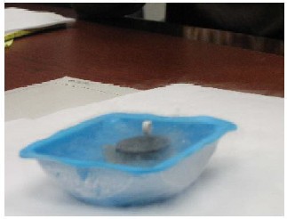
Fig.1 Demonstration of levitation of magnet by superconducting pel- let. The black disk in the blue tray of liquid nitrogen at 77 K (-320.8º F). The object floating in the mist is a small permanent magnet.
Necessary laboratory preparation must be taken dur-
ing the whole experimental procedure.
4 STRUCTURE OF YBCO COMPOUNDS
YBCO crystallises in a defect perovskite structure consisting of layers. The boundary of each layer is defined by planes of square planar CuO4 units sharing 4 vertices. The planes can some times be slightly puckered. Perpen- dicular to these CuO2 planes is CuO4 ribbons sharing 2 vertices. The yttrium atoms are found between the CuO2 planes, while the barium atoms are found between the CuO4 ribbons and the CuO2 planes. This structural feature is illustrated in the figure.
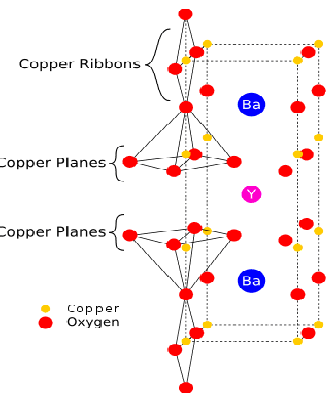
Fig.2 Structure of YBCO compound
Although YBa2Cu3O7 is a well-defined chemical com- pound with a specific structure and stoichiometry, mate- rials with less than seven oxygen atoms per formula unit are non-stoichiometric compounds. The structure of these materials depends on the oxygen content. This non- stoichiometry is denoted by the YBa2Cu3O7-x in the chemi- cal formula. When x = 1, the O(1) sites in the Cu(1) layer are vacant and the structure is tetragonal. The tetragonal form of YBCO is insulating and does not superconduct. Increasing the oxygen content slightly causes more of the O(1) sites to become occupied. For x < 0.65, Cu-O chains along the b-axis of the crystal are formed. Elongation of the b-axis changes the structure to orthorhombic, with lattice parameters of a = 3.82, b = 3.89, and c = 11.68 Å. Optimum superconducting properties occur when x ~
IJSER © 2011 http://www.ijser.org
International Journal of Scientific & Engineering Research Volume 2, Issue 3, March-2011 4
ISSN 2229-5518
0.07 and all of the O(1) sites are occupied with few vacan- cies.
In experiments where other elements are substituted at the Cu and Ba sites evidence has shown that conduction occurs in the Cu(2)O planes while the Cu(1)O(1) chains act as charge reservoirs, which provide carriers to the CuO planes. However, this model fails to address super- conductivity in the homologue Pr123 (praseodymium instead of yttrium). This (conduction in the Copper planes) confines conductivity to the a-b planes and a large anisotropy in transport properties is observed. Along the c-axis, normal conductivity is 10 times smaller than in the a-b plane. For other cuprates in the same general class, the anisotropy is even greater and inter-plane transport is highly restricted.
Furthermore, the superconducting length scales show similar anisotropy, in both penetration depth (.Aab �
150 nm .Ac � 800 nm) and coherence length, (sab � 2 nm, sc
� 0.4 nm). Although the coherence length in the a-b plane
is 5 times greater than that along the c-axis it is quite
small compared to classic superconductors such as nio- bium (where s � 40 nm). This modest coherence length means that the superconducting state is more susceptible to local disruptions from interfaces or defects on the order of a single unit cell, such as the boundary between twinned crystal domains. This sensitivity to small defects complicates fabricating devices with YBCO, and the ma- terial is also sensitive to degradation from humidity.
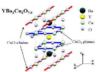
Fig. 3 Crystal structure of YBa2Cu3O7 ("YBCO").The pres- ence of the CuO chains introduces an Ortho-rhombic distortion of the unit cell.
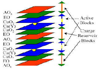
Fig. 4 General structure of a cuprate HTS.
5 RESISTANCE MEASUREMENTS
The idea was to measure the resistance of a YBCO sample from room temperature down to the boiling temperature of liquid nitrogen (77 K). This may be accomplished with two different sample holders. The choice of method de- pends on the availability of the equipment. The can be many methods for this purpose but here only two me- thods are talked about. Method 1 uses the "helium dip- per" while method 2 uses the RMC closed-cycle helium refrigerator. The basic steps for either method are the same: (1) the YBCO thin film sample is mounted on a copper block whose temperature may be varied, (2) a temperature sensor mounted on the copper block is used to determine film temperature, and (3) four spring- loaded, pressure contacts are pushed against the sample and connected to a circuit that will enable to measure the sample resistance. Then the sample temperature was va- ried and the resulting resistances were recorded.
5.1 4-Probe Resistance Cryogenic Dipper
This holder uses a diode temperature sensor, similar to the one in the Janis model DT liquid nitrogen cryostat. If a temperature controller is available, it could be used to monitor the temperature. If not, a 10 )lA current source can be used and the diode voltages are measured.
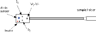
Fig.5 4-Probe Dipper
The "sleeve" must be removed and the sample holder must be inspected. An Ohmmeter is used to determine how the contacts are wired to the BNC connectors at the
IJSER © 2011 http://www.ijser.org
International Journal of Scientific & Engineering Research Volume 2, Issue 3, March-2011 5
ISSN 2229-5518
top of the "dipper."2
The nuts are loosened that hold the contact assembly
down and the contacts are lifted so that there is sufficient
space to slide the thin-film YBCO sample between the
contacts and the copper holder. An insulator is being
sandwiched between YBCO sample and the copper hold- er. Using tweezers and a small screw-driver, the YBCO sample under the contact assembly is positioned. The four contacts are made sure to be used are placed square-
ly on the YBCO film. Gradually the nuts are tighten so that the contacts are forced down against the sample.3
Final adjustment of the contact pressure should be made while monitoring the resistance between all pairs of contacts with an Ohmmeter. With good contacts, the re- sistance between any two is made no more than a few hundred ohms. The contacts and reposition the film are raised if necessary to achieve this.
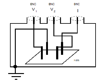
Fig.6 W iring diagram for dipper.
A lock-in amplifier is used to perform the standard 4- probe resistance measurement on the film. Also a large ballast resistor (RB > 10 kQ) in series with the oscillator output of the lock-in to establish a constant current of (roughly) 10 )lA.4 Send this current through the film us- ing two of the contacts is used. The voltage drop (with the lock-in) across the other two film contacts is measured.
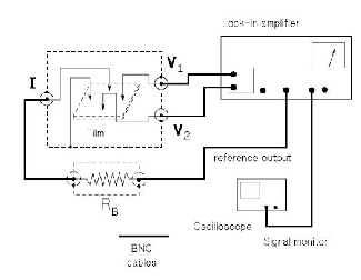
Fig.7 W iring diagram to measure film resistance using a lock-in am- plifier.
While monitoring the film resistance with the lock-in, the "sleeve" must be carefully slide back over the sample holder. Constant attention must be paid to the lock-in reading as the dipper is moved subsequently. It is easy for the contacts to degrade when the sample holder is jarred.
The diode temperature sensor on the dipper is used to measure sample temperature. This is done by hooking up either of the Lake Shore temperature controllers (if avail- able) or by using a 10 )lA current source while measuring the diode voltage. As the sample temperature is lowered periodically the lock-in voltage (proportional to the resis- tance of the YBCO sample) is recorded and temperature (or diode voltage, from which temperature may be de- termined). If available, a p. c. with a 2-channel A/D board or an X-Y recorder can be used to simultaneously record both of these voltages.
The top flange from the helium storage dewar is re- moved and replace it with the dipper/flange.
The pressure relief valve on the helium storage dewar must be opened. As the is dipper slowly lowered into the dewar the cryogenic fluid is boiled, generating gas pres- sure that must be released.
The dipper is slowly lowered into the cryostat, con- stantly monitoring the lock-in voltage and temperature. Ideally a continuous stream of data (X-Y recorder or digi- tized data) is obtained. The sporadic data are also record- ed.
From the obtained data, film resistance versus tem- perature down to 77 K for a measurement current of 10
)lA can be plotted. The onset temperature, Tc, and the
R=0 temperature can be determined too.
IJSER © 2011 http://www.ijser.org
International Journal of Scientific & Engineering Research Volume 2, Issue 3, March-2011 6
ISSN 2229-5518
 ray hits. Measurments conducted in Prof. T. Zhou's lab.
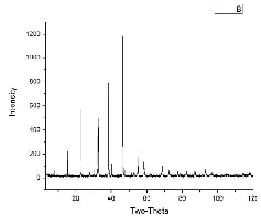
Fig. 8. X-Ray Diffraction pattern of the powder YBCO sample.
Figure 8 shows the X-Ray diffraction pattern of the powder YBCO sample. The YBCO compound prepared following the procedure described in the topic sample fabrication if passed through the X-Ray diffraction tube will give a reading as figure 8.
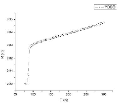
Fig. 9. Resistance as a function of temperature for the sample can be converted to resistivity using the measured sample dimensions.
Figure 9 shows resistance as a function of temperature for the sample can be converted into resistivity using the sample dimensions. Resistance is founf out following the method described in resistance measurement topic.
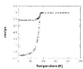
Fig.11. Magnetization measurements in a 100 G field to determine the superconducting fraction of the sample. The zero field cooled portion of the plot can be used to extract the superconducting frac- tion. Measurements were conducted at Prof. M. Greenblatt's Lab. at Rutgers University.
Figure 10 and 11 shows different other readings taken on the sample materials.
ACKNOWLEDGMENT
We would like to thank Prof. Sekh Abdur Rob for his continuous support and motivation to carry out our work. He has provided us with tremendous encourage- ment with his knowledge of superconductivity. We are truly grateful towards him.
REFERENCES
[1] Roland Hott2, Reinhold Kleiner3, Thomas Wolf2 and Ger- trud Zwicknagl4. 2005. “Superconducting Materials — A Topical Overview”, Publisher: Springer Berlin Heidelberg.
[2] High-Temperature Superconductivity in Cuprates. The Nonlinear Mechanism and Tunneling Measurements Series: Fundamental Theories of Physics, Vol. 125, Mourachkine, A.
2002, 340 p., Hardcover
[3] Engel, S., Thersleff, T., Hühne, R., Schultz, L., Holzapfel, B. Enhanced flux pinning in YBCO layers by the formation of nano- sized BaHfO3 precipitates using the chemical deposition method. [4] Knoth, K., Engel, S., Apetrii, C., Falter, M., Schlobach, B., Hühne, R., Oswald, S., Schultz, L., Holzapfel, B. Chemical solution deposition of YBa2Cu3O7-x coated conductors.
[5] Falter, M., Demmler, K., Häßler, W., Schlobach, B., Holzapfel, B., Schultz, L. Chemical solution deposition (CSD) of YBa2Cu3O7-x films and oxide buffer layers by dip coating.
[6] http://hyperphysics.phy-astr.gsu.edu/hbase/Solids/scond.html
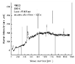
Fig.10. Raw Raman data with sharp singlepoint spikes from cosmic
IJSER © 2011 http://www.ijser.org