International Journal of Scientific & Engineering Research, Volume 5, Issue ŝ, Ju¢-2014
ISSN 2229-5518
Power and Delay Characterization on
Full Adder Performance
Bhuvaneshwari.N.K.
—————————— ——————————
1 Introduction
293
Adder is one of the most important
components of a CPU (central processing unit), Arithmetic logic unit (ALU), floating point unit and address generation like cache or memory access unit use it. In addition, Full- adders are important components in other applications such as digital signal processors (DSP) architectures and microprocessors. Arithmetic functions such as
‘addition’, ‘subtraction’, ‘multiplication’ and
‘division’ are some examples, which use ‘adder’ as
a main building block. As a result, design of a
high-performance full-adder is very useful and important*2+.
As we know there are different types of adders. It includes the CMOS standard adder, the mirror adder, the multiplexer-based adder, the transmission gate based adder, the hybrid full adder, the majority full adder etc*3+. Here, the popular adder structures are implemented in the
CMOS 45-nm, 90-nm and 180-nm process
technology and analyzed for performance, power, area and delay. The adders selected for the implementation are the standard adder, the data driven dynamic logic and the split-path data driven dynamic logic. Each of the full adders are classified according to the logic function that is realized. Using this approach we have presented an analysis of the possible impact of logic function choice and not just circuit choice on the performance of the final adder*3+.
Three different adder functions are realized using the proposed data driven dynamic logic (D3L) and split-precharge data driven dynamic logic (sp-D3L). These implemented full adders can find its application in a ripple carry adder (RCA) and Wallace Tree multiplier to carry out the delay, power and power-delay product on the performance of full adders as well as the systems that employ them*3+.
————————————————
IJSER © 2014 http://www.ijser.org
International Journal of Scientific & Engineering Research, Volume 5, Issue ŝǰȱ ¢ȬŘŖŗŚ
ISSN 2229-5518
294
The performance of a full adder circuit
depends on the logic function realized using the particular design style. For instance, a standard CMOS implementation allows circuits to achieve a reasonable power delay product (PDP). Dynamic implementations on the other hand may yield an extremely fast design but end up paying higher costs in the overall power consumption*3+. D3L and sp-D3L are two design styles which allow high performance dynamic circuit design without the additional power consumption in the clock distribution network. Thus these styles form interesting implementation strategies for realizing high performance, power-efficient full adders*3+.
2 PROPOSED FULL ADDERS
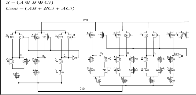
During the design of an adder we have to make two choices in regard to different design abstraction levels. One is responsible for the adder’s architecture implemented with the one-bit full adder as a building block. The other defines the specific design style at transistor level to implement the one-bit full adder*1+. The one-bit full adder used is a three-input two-output block. The inputs are the two bits to be summed A and B, and the carry bit Ci, which derives from the calculations of the previous digits. The outputs are the result of the sum operation and the resulting value of the carry bit Cout.
IJSER © 2014 http://www.ijser.org
International Journal of Scientific & Engineering Research, Volume 5, Issue ŝǰȱ ¢ȬŘŖŗŚ
ISSN 2229-5518
295
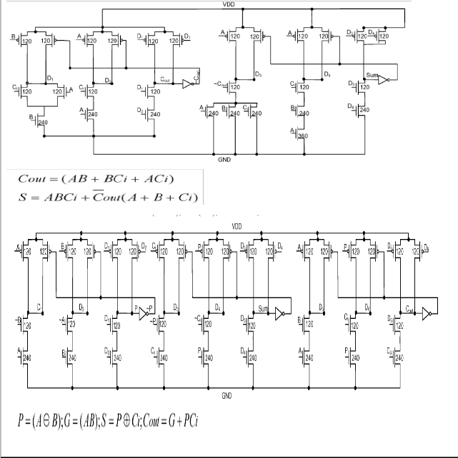
Fig. a. sp-D3L implementation of three full adder functions.
For the simulation of a full adder, there
are two important facts. One is the type of design style ued for the implementation and the other is the realized logic function. The first figure represents the standard CMOS implementation which allows the circuit to achieve a good power delay product. The number of transistors used for the CMOS standard adder is 40. The circuit is analysed by assigning a 1 bit value for the inputs. Here, if the circuit makes use of more number of transistors then the circuit gives more delay. So,
the sizing of the transistors plays a very important
role. Hence, the sizing of the transistors is done in the next two adders, i.e. the Dynamic implementations. The Dynamic implementations are fast but the power consumption is high. The second and third figure is the D3L and sp-D3L are the two design styles for realizing the high performance, power efficient full adders. And in sp-D3L adder, we make use of the GENERATE and PROPOGATE signals for the best performance of the adder circuit.
IJSER © 2014 http://www.ijser.org
International Journal of Scientific & Engineering Research, Volume 5, Issue ŝǰȱ ¢ȬŘŖŗŚ
ISSN 2229-5518
296
The sizing of the transistors plays a very
important role in the optimization of the circuit performance, power consumption, noise margins, fan-in, fan-out etc. so, the sizing of the transistors gives a best power-delay product by maintaining the drivability of the adders. So, the D3L adders are sized to reduce the delay. The adder circuits are implemented in CMOS 90nm and 180nm technology. The main drawback of these adders is the high power consumption due to large number of transistors and multiple paths to the ground. Here the table represents the comparision of the full adders in terms of delay, power and power delay product.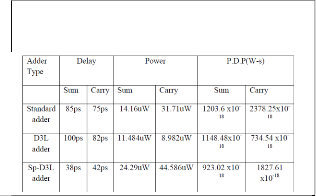
The power, delay and the P.D.P in the earlier paper is done in IBM 90nm process *3+ and the values are tabulated in the below table table 1.
Table 1. The Sum and Carry Delays, Power and the P.D.P for all the three adders in 90nm IBM technology.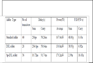
Table 3. The Sum and Carry Delays, Power and the P.D.P for all the three adders in 90nm CMOS technology.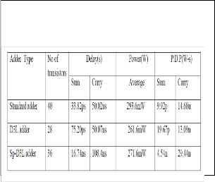
Table 4. The Sum and Carry Delays, Power and the P.D.P for all the three adders in 180nm CMOS technology.
Now, the adders are designed and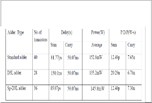
simulated in Cadence Virtuoso using GPDK tool kit under laboratory conditions and compared and tabulated below in table 2, table3 and table4.
Table 2. The Sum and Carry Delays, Power and the P.D.P for all the three adders in 45nm CMOS technology.
3 RESULT
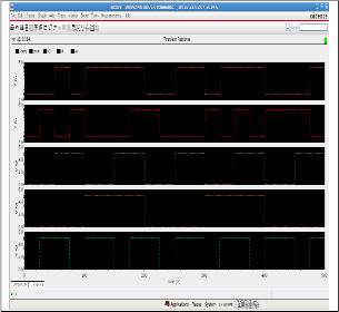
![]()
When we compare the three different adders, the D3L adder uses less number of transistors than the other two adders. Hence, the delay of the D3L adder is less and the consumption of the power too, is less when compared to the other adders. So, the P.D.P is less for the D3L adder. When compared to 90nm CMOS technology, 180nm has more delay, consumes less power. The adder with more number of transistors has more delay and consumes more power than the adder with the less number of transistors. And the comparision is done in the table.
Below represents the simulation results of the proposed full adders.
IJSER © 2014 http://www.ijser.org
International Journal of Scientific & Engineering Research, Volume 5, Issue ŝǰȱ ¢ȬŘŖŗŚ
ISSN 2229-5518
The sp-D3L adders implemented here has the speed advantage however it consumes more power. The power consumption can be reduced, but the pre-charge propogation path delay affects the speed performance of the adder.
ACKNOWLEDGMENT
I wish to thank Dr. V. Shridhar, P.E.S. College of Engineering, Mandya, for helping me to finalize the nature and site of project and for his valuable guidance, constant encouragement, support and suggestions for improvement.
REFERENCES
297
The Standard, D3L and sp-D3L adder in
45nm technology has a average sum delay of
81.77ps, 150.1ns and 85.07ps respectively and
average carry delay of 50.07ns. These adders consumes the average power of 152.8mW,
135.2mW and 145.8mW respectively. The Standard, D3L and sp-D3L adder in 90nm technology has a average sum delay of 33.82ps, 75.20ps and 16.74ns respectively and average carry delay of 50.02us,
50.07ns and 108.4ns respectively. These adders consumes the average power of 293.6mW,
261.6mW and 271.6mW respectively. And at last, The Standard, D3L and sp-D3L adder in 180nm technology has a average sum delay of 286ps,
284.6ps and 16.72ns respectively and average carry delay of 50.26ns, 50.64ns and 91.74ns respectively. These adders consumes the average power of
167.9mW, 136.8mW and 179.2mW respectively.
4 CONCLUSION
The new split path Data Driven Dynamic Logic Implementation of the full adder is strong in terms of both performance-power-efficiency and drivability. This is very efficient when low power constraints are mandatory. Due to small, identically loaded gates the full adders designed using PROPOGATE and GENERATE functions, the full adder is observed to be the best in the performance.
*1+ Massimo Alioto and Gaetano Palumbo.
*2+ “On the Design of High-Performance CMOS 1- Bit Full Adder Circuits.” International Conference on VLSI, Communication & Instrumentation (ICVCI) 2011. Proceedings published by International Journal of Computer Applications® (IJCA).
*3+ Sohan Purohit and Martin Margala, “Investigating the Impact of Logic and Circuit Simulation on Full Adder performance”, IEEE Trans. on Very Large Scale Integr.(VLSI)Syst.,vol.20, no.7, July 2012.
*4+ Yingtao Jiang, Abdulkarim Al-Sheraidah, Yuke Wang, Edwin Sha, and Jin-Gyun Chung “A Novel Multiplexer-Based Low-Power Full Adder.” IEEE transactions on circuits and systems, vol. 51, no. 7, july 2004.
*5+ K. Navi, O. Kavehie, M. Rouhulamini, A. Sahafi, and S. Mehrabi, “A novel CMOS full adder,” in Proc. 20th Int. Conf. VLSI Design, 2007, pp. 303–
307.
*6+W.R.Rafati,S.M.Fakhraie,and K.C.Smith,“Low-
752–755.
IJSER © 2014 http://www.ijser.org