International Journal Of Scientific & Engineering Research, Volume 3, Issue 6, June-2012 1
ISSN 2229-5518
Abstract— Multilevel inverter technology has emerged recently as a very important alternative in the area of high -power medium-voltage energy control. In multi level inverters the most important topologies like diode-clamped inverters (neutral-point clamped), capacitor-clamped (flying capacitor), and cascaded multi cell with separate dc sources. Diode-clamped inverter results in the low frequency voltage ripple in the NP, which is the point between the two dc-link capacitors. This explores the fundamental limitations of the NP voltage balancing problem for different loading conditio ns of three-level voltage source converters. It also represents that the most relevant control and modulation methods developed for the space-vector modulation technique. Design of L and LCL filter is done for three level diode clamped inverter connected to grid. Three phase VSI are switched by these PW M pulses to improve the output waveforms of the three level diode clamped inverter connected to grid using filters. The procedure for designing an LCL- filter is proposed and verified by simulations. This paper proposed method PW M waveforms are generated by SVPW M technique using MATLAB/SIMULINK and L and LCL filter is designed connected to grid.
—————————— ——————————
The area of multilevel power conversion can still be considered young. In 1980, early interest in multilevel power conversion technology was triggered by the work of Nabae, etal., who introduced the neutral-point-clamped (NPC) inverter topology. It was immediately realized that this new converter had many advantages over the more conventional two-level inverter. Subsequently, in the early nineties the concept of the three-level converter was extended further and some new multilevel topologies were proposed. At the present time, the majority of research and development effort seems to concentrate on the development of three classes of converters: the diode-clamped multilevel converter, the multilevel converter with cascaded single-phase H-bridge inverters, and the multilevel converter known as the flying capacitor converter, or sometimes as the imbricated cells multilevel converter. As mentioned, the three-level NPC converter was the first widely popular multilevel topology.
The introduction of the NPC converter, the original topology was extended to a higher number of levels using the same principle of diode-clamped intermediate voltage levels.
The concept of space voltage vectors corresponding to various switching states has been applied to study the impact of various switching states on the capacitor charge balancing in almost every paper discussing the SVM approach. An advantage of the SVM is the instantaneous control of switching states and the freedom to select vectors in order to balance the NP. Additionally, one can realize output voltages with almost any average value by
using the nearest three vectors, which is the method that results in the best spectral performance. The primary
constraint in devising SVM (as is the case with in most multilevel modulation techniques) involves minimizing the harmonic content of the output PWM waveform while at the same time maintaining the capacitor charge balance. With respect to modeling and control of three level converters, the dominant approach is to divide and conquer. The phase legs are treated essentially as voltage sources while the charge balance becomes part of the modulator, which selects between the redundant switching states in order to maintain the charge balance in the split dc-link capacitors.
In this paper Simulink model of a three-level converter that included the NP voltage using SVPWM technique is done and the design of L and LCL filters was developed and connected to grid using MATLAB/Simulink [8] to give pure sinusoidal waveform to grid.
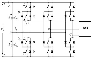
Switching states that are shown in Fig.1 can represent the operating status of the switches in the three-level NPC inverter. When switching state is ‘1’, it is indicated that upper two switches in leg A connected and the inverter terminal voltage VAZ, which means the voltage for terminal A with respect to the neutral point Z, is +E, whereas ‘-1’ denotes that the lower two switches are on, which means VAZ = -E. When switching state ‘0’, it indicates that the inner two switches S2 and S3 are connected and VAZ =0 through the clamping diode, depending on the direction of the load current ia.
IJSER © 2012 http://www .ijser.org
International Journal Of Scientific & Engineering Research, Volume 3, Issue 6, June-2012 2
ISSN 2229-5518
Fig 1: Three-level Neutral Point Clamped inverter [1].
When DZ1 is turn on, the load current will be positive and the terminal A will be connected to the neutral point Z through the conduction of DZ1 and S2. Table 1 shows switching status for leg A. Leg B and leg C have the same concept.
Table.1 Definition of Switching States
represented by three letters in square brackets for the inverter phases A, B, and C. The voltage has four groups.
a. Zero vector (V1, V2, V3), representing three switching states [1 1 1], [-1 -1 -1] and [0 0 0]. The magnitude of V1, V2, and V3 is Zero.
b. Small vector (V4 to V15), all having a magnitude of Vd/3.
Each small sector has two switching states, one containing
[1] and the other containing [-1] and they classified into P- or N- type small vector.
c. Medium vectors (V17, V19, V21, V23, V15, V27 ), whose magnitude is ![]() Vd.
Vd.
d. Large vectors (V16, V18, V20, V22, V24, V26), all having a
magnitude of ![]() Vd.
Vd.
The space vector diagram that is shown in Figure.4 can be used to calculate the time for each sector (I to VI). Each sector has four regions (1 to 4), with the switching states of all vectors.
By using the same strategy that was used in chapter two, the
sum of the voltage multiplied by the interval of choose space vector equals the product of the reference voltage Vref and sampling period TS. To illustrate, when reference voltage is located in region 2 of sector I then the nearest vectors to reference voltage areV5 ,V17, and V7 as shown in Fig. 2, and the next equations explain the relationship between times and voltages :-
Space vector pulse width modulation (SVM) is quite different from the PWM methods. With PWMs, the inverter can be thought of as three separate push-pull driver stages which create each phase waveform independently. SVM however treats the inverter as a single unit. Specifically the inverter can be driven to eight unique states. Modulation is accomplished by switching the state of inverter. SVM is a digital modulation technique where the objective is to generate PWM load line voltages. This is done in each sampling period by properly selecting the switching states of inverter and calculation of the appropriate time period for each state.
Three switching states [1], [0] and [-1] can represent the operation of each leg. By taking all three phases into account, the inverter has a total of 27 possible switching states. Table 3 shows the possibility of three phase switching states that are![]()
![]()
![]()
![]()
![]()
![]()
![]()
![]() , (1)
, (1) ![]()
![]()
![]()
![]()
![]()
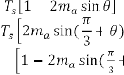
![]() (2)
(2)
Where Ta, Tb and Tc are the times for V5, V17 and V7
respectively.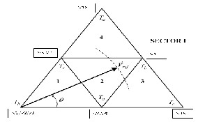
Fig 2: Voltage vector and their times[4].
![]()
![]()
From Fig. 2 voltage sectors V5 ,V7 andV17 can be observed as follow:-![]()
![]()
![]()
![]()
![]()
, ![]() ,
, ![]() ,
,
IJSER © 2012 http://www .ijser.org
(3)
International Journal Of Scientific & Engineering Research, Volume 3, Issue 6, June-2012 3
ISSN 2229-5518
By substituting equation (3) into (1), we get![]()
![]()
![]()
![]()
![]()
![]()
![]()
![]()
![]()
![]()
3 = ( + ) (4)
From equation (4) real part and imaginary part can be
determined by following Equations![]()
![]()
![]()
![]()
![]()
![]()
![]()
![]()
![]()
![]() (5)
(5) ![]()
![]() (6)
(6)
By solving equation (5) & (6) with the equation for total time
TS = Ta + Tb + Tc, for 0 ≤ Ѳ ≤ π/3.
![]()
![]()
![]()
![]()
![]()
![]()
![]()
![]()
![]()
![]()
![]() (7) Where ma is the modulation index and can be expressed as follow:-
(7) Where ma is the modulation index and can be expressed as follow:-
The relationship can be observed between Vref Location and time shown in fig 3. By assuming the location of Vref at point
Q located at the center of region 3. Because the distances for the nearest vectors V5 and V7 , V17 from Q are the same, the times for these vectors should be identical.![]()
![]()
![]() (8)
(8)
The maximum value for V ref can be derived at medium
vector voltage![]()
![]()
![]() (9)
(9)
And the modulation index can be given as below
0 ≤ ![]() ≤ 1
≤ 1
The equations for the calculation of times for Vref in sector I
can are given in table 4 as below.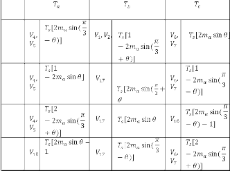
Table 2: Time calculation for Vref in sector I
Reg ion
1
2
)−1]
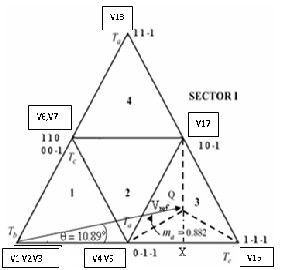
Fig 3: An example to determine the relationship between the location of V ref and times[6].
Three triangles in region 3 are equilibrium triangles. From triangle V0 ,X, and Q Vref =0.5Vd , and θ = 10.89o . By substituting in equation (6), ma = 0.8 and Ta = Tb = Tc =0.3333Ts from the equations in table.4.
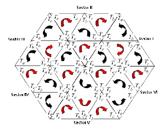
By considering the switching transition and using sequences direction, shown in Fig.4. and Fig.5, the direction of the switching sequences for all regions in six sectors can be derived and the switching orders are known, which are obtained for each region located in sectors I to VI, if all switching states in each region are used.
3
]
4
]
The calculated times remain same for sectors (II to VI) shown in
Table 2.
IJSER © 2012 http://www .ijser.org
International Journal Of Scientific & Engineering Research, Volume 3, Issue 6, June-2012 4
ISSN 2229-5518
UGm – amplitude of grid voltage, Im – amplitude of current,
ω - angular frequency of the grid.
The application of a LCL low pass filter (Fig.6) with a relatively small filter size and a good decoupling of the filter performance from grid impedance variations provides a good performance. It can be seen that the ac filter can be smaller / less heavy for a three-level topology for any desired current ripple value or harmonic spectrum. Due to the quadratic dependency of ripple current and losses the application of a three-level converter will result in substantially smaller losses in any given inductance.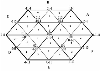
Fig 4: Switching sequence for three-level SVPWM inverter[4] 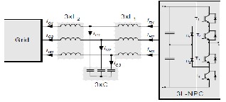
Fig 6: Diagram of a three-phase LCL-filter connected between grid and 3L-NPC PWM rectifier.
This topology consists on just an inductive filter L connected in series with the converter. Although being the topology with the fewer number of components the system dynamics is poor due to the voltage drop across the inductor causing long time responses.
Fig 5: Sectors and their regions for three-level inverter [10]
The reduction of the current harmonics around switching frequency and multiplication of switching frequency is done to achieve compliance with grid codes as IEEE 519-1992. High inductance values can achieve this goal; however, inductor is bulky, expensive and will limit the converter dynamics as well as the total operating range. The voltage drop across the inductance is controlled by the fundamental component of the PWM converter voltage with its maximal amplitude limited by the DC-link voltage. Consequently, a high current through the inductance requires either a high dc-link voltage or a low inductance. The maximal inductance can be determinate to![]()
L< (10)
Grid side inductance =100 [mH] Converter side inductance =100[mH] Capacitor (star connection) =5 *μF+
Table 3: modulation index versus THD (%) for LCL filter
Where
udc – dc- link voltage,
IJSER © 2012 http://www .ijser.org
Table 4: Modulation index versus THD (%) for L filter
International Journal Of Scientific & Engineering Research, Volume 3, Issue 6, June-2012 5
ISSN 2229-5518
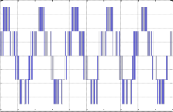
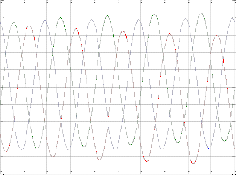
The output line to line voltage waveform for three phases three level inverter in figure 9.
800
600
400
200
0
-200
-400
-600
-800
0 0.01 0.02 0.03 0.04 0.05 0.06 0.07 0.08 0.09 0.1 time(s)
Table 3 & 4 gives the variation of modulation index versus total harmonic distortion [THD] for LCL and L filter.
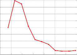
Figure 7 and figure 8 shows the variation of Total Harmonic
Distortion (%) versus modulation of LCL & L Filters.
Fig 9: The output line to line voltage waveform for three phase three level inverter
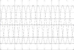
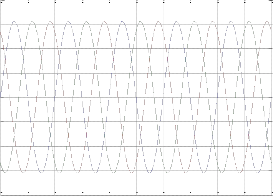
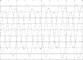
Figure 10 and figure 11 shows the grid side Phase voltage and current of LCL filter respectively. Figure 12 and figure 13 grid side Phase voltage and current of L filter respectively.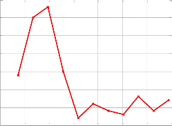
5
4.5
4
3.5
3
2.5
2
200
150
100
50
0
-50
-100
-150
1.5
0.4 0.5 0.6 0.7 0.8 0.9 1 modulation
Fig 7: THD% v/s modulation of L filter
-200
0 0.01 0.02 0.03 0.04 0.05 0.06 0.07 0.08 0.09 0.1
time(s)
Fig 10: Grid side Phase voltage of LCL filter
11
10
9
8
7
6
5
4
3
0.4 0.5 0.6 0.7 0.8 0.9 1
modulation
Fig 8: THD% v/s modulation of LCL filter
50
40
30
20
10
0
-10
-20
-30
-40
-50
0 0.01 0.02 0.03 0.04 0.05 0.06 0.07 0.08 0.09 0.1 time(s)
Fig 11: Grid side Phase current of LCL filter
IJSER © 2012 http://www .ijser.org
International Journal Of Scientific & Engineering Research, Volume 3, Issue 6, June-2012 6
ISSN 2229-5518
200
150
100
50
0
-50
-100
-150
-200
0 0.01 0.02 0.03 0.04 0.05 0.06 0.07 0.08 0.09 0.1
time(s)
Fig 12: Grid side Phase voltage of L filter
50
40
30
20
10
0
-10
-20
-30
-40
-50
controls, and applications‛. IEEE Transactions On
Industrial Electronics, Vol. 49, No. 4, August 2002.
[2] Kalpesh H. Bhalodi, and Pramod Agarwal, ‚Space Vector Modulation with DC-Link Voltage Balancing Control for Three-Level Inverters‛ International Journal of Recent Trends in Engineering, Vol 1, No. 3, May 2009.
[3] Katsutoshi Yamanaka, Ahmet M. Hava, Hiroshi Kirino, Yoshiyuki Tanaka, Noritaka Koga, and Tsuneo Kume,” A
Novel Neutral Point Potential Stabilization Technique Using the Information of Output Current Polarities and Voltage Vector‛,IEEE Transactions on Industry Applications, Vol 38 ,No.6, November/December 2002.
[4] Abd Almula G. M. Gebreel, ‚Simulation and
implementation of two level and three-level inverters by
Matlab and RT-lab‛. The Ohio State University 2011.
[5] P. Satish Kumar 1 J. Amarnath 2 S.V.L. Narasimham 3 ‚A
Fast Space-Vector Pulse with Modulation Method for Diode-Clamped Multi-level Inverter fed Induction Motor‛. IEEE Trans. on Power Electronics, Vol. 18, no. 2, pp.604-611,March 2003,
[6] Ayse KOCALMIS, Sedat SÜNTER, ‚Modelling And Simulation of A Multilevel Inverter Using Space Vector Modulation Technique‛, Asian Power Electronics Journal, Vol. 4 No.1 April 2010.
[7] Hind Djeghloud, Hocine Benalla,‛ Space Vector Pulse
Width Modulation Applied to the Three-Level Voltage
Inverter‛ Electrotechnic's Laboratory of Constantine
0 0.01 0.02 0.03 0.04 0.05 0.06 0.07 0.08 0.09 0.1
time(s)
Fig 13: Grid side Phase current of L filter
9 CONCLUSION
An implementation done concerning the application of the SVPWM control strategy on the three-level voltage inverter for L & LCL filters was presented using MATLAB/SIMULINK. Designing of L and LCL filters is done to smooth the inverter output which is connected to grid.
This aimed on the one hand to prove the effectiveness of the
SVPWM in the contribution in the switching power losses
reduction and to show the advantage of multilevel inverters that carry out voltages with less harmonic content’s injection than the comparable two-level inverters on the other hand and design of filters to give sinusoidal output to grid. The obtained simulation results were satisfactory. As prospects, future experimental works will validate the simulation results.
[1] José Rodríguez, Jih-Sheng Lai, and Fang Zheng
Peng,‛Multilevel Inverters: A Survey of topologies,
Mentouri-Constantine University, Constantine 25000,
Algeria.
[8] Nikola Celanovic, Fred C. Lee, Douglas J. Nelson, ‚Space Vector Modulation and Control of Multilevel Converters‛. September 20, 2000.
[9] Marco Liserre, Frede Blaabjerg, Steffan Hansen.‛Design and Control of an LCL-filter based Three-phase Active
Rectifier‛.
[10] Samuel Vasconcelos Araújo, Alfred Engler, Benjamin
Sahan, Fernando Luiz Marcelo Antunes. ‚LCL Filter design for grid-connected NPC inverters in offshore wind turbines‛. The 7th International Conference on Power Electronics. October 22-26, 2007 / EXCO, Daegu, Korea

IJSER © 2012 http://www .ijser.org
International Journal Of Scientific & Engineering Research, Volume 3, Issue 6, June-2012 7
ISSN 2229-5518
College, Bagalkot. His areas of interest are power electronics, Renewable Energy, FACTS. He is member of IEEE.
Masters degree in Power and Energy Systems from NITK
Surathkal. He is presently working as Senior Lecturer in the Department of Electrical and Electronics Engineering, Basaveshwar Engineering College, Bagalkot, India since 1997. He has published 05 journals at National and International Conferences. His main reaserch interests are Power Electronics and Drives. He is member of IEEE.
2000 respectively. His areas of interest include Wind Energy Systems, Computer Applications to Power System, Microprocessor Based System Design, and Computer Relaying. He won the "Outstanding IEEE Student Branch Counsellor" award for the year 1996 at Basaveshwar Engineering College, Bagalkot, Karnataka, India. Presently he is working as Professor in the department of E&E at Basaveshwar Engineering College, Bagalkot.
IJSER © 2012 http://www .ijser.org