International Journal of Scientific & Engineering Research, Volume 3, Issue 1, January-2012 1
ISSN 2229-5518
ON THE INTEGRATION FOR THE ELECTRONIC TREND OF TATICAL GRAPHICS
Ahlam T.Al-Sarraf
Abstract-- Currently, many scientists believe in the fact that electronics as a vast modern discipline needs relevant tools and tactics to develop its already living syst-ems. This technical note contains an everywhere path for the development of computing artificial intelligence techniques, software design and database descriptions mark the human needs for a varity of computing functions:(a) Among which training and testing knowledge of tactical situations (b) Better planning and decision for planning situations interfacing tactical artificial intelligent systems.(c) Providing an experiment for studding tactical decision making. In fact, this studying aims at an-swering some queries found in the above question like what can architects in electronics provide in tactical graphics.This humble research paper is being undertaken to give a workable answer to some or part of these queries found in the area of electronics which is hoped to be reliable source within variety of computing fields. It will provide an acceptable answer to what is being asked about integration between soft and hardware made to develop tactical graphics in electronic. It has become now possible for the designer to connect the personal computer (Buses) with any outside apparatus by means of designing a suitable card (ADAPTER) fixed on the(EXPA-NSION- SLOT).Thus,the primary aim of this study is to develop reprogrammable and prototype boards aiming producing some reliable features suitable for
final use graphic cards.
1-INTRODUCTION
The great role of our age of information has had its clear impact on the mo- dern immense development in the technology of computer, in the fact that ele- ctronics as a modern discipline engaged the development of relevant tools
and tactical to insure and facilitate the role and use of its living systems. This role is not limited only to introducing computer systems and their programs rather than the programming language statement rules and drawing design programs We believe that the above note contains an everywhere path for the develop-ment of computing artificial intelligence technique and designs . Many of whi-ch are invested in administration to establish devices of
shopping propaganda and advertisement,which have been enlarged to become greater in the industri-al,scientific and technological fields.It seams that such important role is rather neglected by us the Arabs.The economical sector and the industrial section oc-cupy a vital part in the ability of computer technology since they are directly connectend with the control system,statements resulting from measurements process and adjustment.Soft ware design and databased descriptions mark the human needs for a variety of computing functions such as training and testing knowledge for tactical situations ,better planning decisions inter-facing tactical artificial intelligent systems and providing prototype experim-ent for studying tactical decision making.Yet their astonishing development and surprising per-formance together with their wide spread, made them a pr-oper model choice in this vast area of knowledge.
Here lies the important of this humble study. We consider it as an encouraging beginning concerning the suitability of com-puting cards design,since it does not represent a clue for setting up controlling systems. It is considered as a
try to join the personal computer with the out-side surrounding atmosphere with the hope to be a suitabl guide the universi-ty students to set up or form some advantageous control-ing system for their own purpose during their study of tactical design.
2- PREVIOUS STUDIES-
Katz(1989) discusses the graphic tactic to enhance the architectures for high performance computing. Similarly, King Kuose and Rose (2005)describe ways to imp-rove an accurate performance model, using a hierarchy of programmable interconnect to allow for logic blocks to be interconnected as needed by the system designer. Moreover,in digital circuit,a flip-flop is a kind of bistable multivibrator an electronic circuit which has two stable states and thereby is capable of sering as one bit of memory.Today,KuoseRose2005 view term flip-flop as one bit memory generally denoted nontransparent (clo- cked or edge-triggered)devices while the simpler transparent once are often re-
ferred to as latches. It is realized that before the development of low-cost in-
tegrated circuits, chains of multivibratorsare found in use as frequency divid- ers. This technique was used in early electronicorgans ,especially insome app- lication of early version system.A transition from one state of minimal free en- ergy requires some form of activation energy to penetrate the barrier Kuose (Ibid )view the time,it take as usually attributed to the relaxation time,since the sy-stem will relax into the next state of lowest energy again,which will be de-fine in such situation. Wolf (Ibid) and nutt (Ibid) believe that the above roles and activities have been greatly inlarge to include scientific industrial and vast technological fields . Yet, science and engineering have been greatly develop-ped the invention of com-puting devices, which will help scientists and resear-ch students to collect, manipulate and interpret relevant data with much greater speed, accuracy and precision.
3- AIM OF THE PAPER
The primary aim of this paper to answer the question of what can archit-ects, electronics and computers offer to people with vision impairments. In fact, this ques-tion includes immense roles of the endless information available in these days and the noticeable development in the technologyof computers,which are not only made to introduce operating systems and their feeding programs like,but are originally utilized to develop different types of administration in human activities made in rel-evance toshopping,propaganda advertisement and the like. Here lies the importance of this paper with its remarkable aim in this study to encourage a start concerning suitable cards design. Humbly speaking,this research paper isn’t made to present a noticeable process for setting up sophisticated controlling design or watching syste-ms for we consider it a try to join the personal computer with the outside human activities. In the same time, a tactical graphics study TGS that makes a design tactical source hardware,architecture and standard for graphics card leading primarily for targeting free software,source operating system. Hence,this study will be developing programmable and prototype boards aiming at producing some noticeable featured and end _user graphics cards.
4- PROCEDURAL METHODOLOGY-
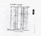
The procedural methodology and function of the circuit relevantly used in this paper is mainly based on the processes of conversion of digital signal provided by the computer into analog signal used widely within industrial application. Thus,all components of the procedural principle are built on the cards known asXt board in order to facilitate the connection. This card is composed from 62 pins based on two directions A and B where each direction is composed of 31 pins devoted to transfer or to achieve the
IJSER © 2012
http://www.ijser.org
International Journal of Scientific & Engineering Research, Volume 3, Issue 1, January-2012 2
ISSN 2229-5518
communication between the computer and the card . The path way used in the computer is of the type ISA (Instruction Set Architecture ). It is one of the ad-
equate methods known to be used in connection and communication.
4-1 Contents for Methods-
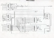
It is realized that the adequacy of the procedural methods need the following componential units (see the diagram,above),U1 and U2(74lS244, OCTAL BUFFERS) are needed to accomplish a protection circuit between the input and output represented by the computer concerning the out put of data to the card. U1 and U2 are considered as the component of the circuit which are made of three case buffers. The interface buffering require several additional integrated circuit to be added to the circuit load of computer,this method is hope to eliminate any potential problem from far out which is measure of the number of logical gate inputs driven by the current from a sig-nal gate output. This buffering system is accomplished by using three74LS244s chips which is in fact an octal buffer and line driver with three state outputs,is made to provide unidirectional buffering for sixteen computer times. On the other hand,the chip is design to improve both the performance and density for three state memory of address,clock and bus- oriented receivers and transmitters.
4-2 U1 and U2 function-
The main function of U1 andU2 is to provide protection circuit between the inputs and outputs represented by computer made in relevance to the output of data to the card. They are consist of(20) pins for each. pin(1)and(2)represent the enabling concerning buffer U1.pin(10) represent the ground,pin(20) is Vcc , he remain of pins are fundamentalling functioning as input of the addresses fromA3-A9,as well as the signal enabling(AEN). Besides,U2 function is to represent buffer of the addresses from A0, A1 and A2 on the pin(13,15 and
17)respectively. In addition, the signal LOR is connecting to pin(2) and LOW
connect to pin(4),beside other unused signal.
4- 3 U3 and function-
U3(74LS245,OCTAL TRANSCEIVERS) rrepresents a buffer ascribed by two directions(asynchronous bidirectional buffering for eight data lines). It is thought that this type of buffering willsend data to computer only when the computer is Reading(R) data and will send data from computer to the card when the computer is perform- ing (W)write function. Data is realized as the information which can be transferred from the computer to the card and vice versa function.Therefore, pin (1) and (19) are supposed to enable the processes of both reading and writing.
4-4 U4 and U5 function-
U4andU5(74LS337,LATCH WITH 3-STAGE OUTPUT) are electronic circuit used to store the data for certain period of time ,and these circuit are made to digital (D) flip- flops where each of them contains (8)D flip flops has a special function to store one bit of data. They are contain buffers for input/output data from latch to D/A co-nverter.The function of this latch has to suitable enough to enable the process of making the output data,represented by pin(11)withinU4andU5.Two latches used in here are used to represent one of the two axis for each i.e one for x-axis and the other y-axis. Whereas the enabling signal is taken fromU8which is functioning as a decoder to the relevant addresses coming from the three input to 8 input (Y0---Y7). Infact,the above processing try is made to solve one of the serious problems faced the res-earch.
Since,it is found that above design card will of the main card ,thus,the decorder is
used to ignite the latch after inserting it on not gate,where the output decoder is low and the enabling of latch is high,hence,one of primary problems we faced during the preliminary operation of this cct. Pin(14)and(15)fromU8hold the following addresses(318 and 319). These two addresses are found to enter theORgate,where each one of them allows entering a gate with the addition 0 signal LOW. For we are using the processes of reading only.
4-5 U6 and U7 function-
U6 and U7 made to operate adequately. Hence, these function as the circuit of conversion of the digital signals to analogs to operate with the capacity of 8 bit input concerning the complete circuit. On the other hand, the output is realized on pin 5 from ic circuit. Accordingly,we easily get two different signal converted from di- gital form into analog signals.The output circuit is directly connected to OSC. which has the capable function.
4-6 U8 function-
U8(74LS138,DECODER)is made to operate directly via two different signals. The first signal is realized to take the addresses(A3 AND A4)which enter to a binary input AND gate. Therefore ,the output of the gate goes to pin(6)withinU8. The second signal take the addresses(A5,A6,A7,A8,A9 and AEN),which represent the outp- ut of U1. Thus, the use of gate NOT, AND,will help to the output of the gate. Hence,the process of writing is achieved by this output representing the second pin of the enabling decoder as well as the enabling of U3 to achieve the process of writing. For the functional operations of U6and U7(Zn 423,DIGTAL TO ANALOGE)all the data sent from the computer to the
latch are seen in the form of digital entities and in order to convert these into analog signals,which display the analogue signals in ad-ditional to proper measuring of their amplitude added to the measuring of the time factor using the
validity of axis as well as capabilities.
4-7 Finally Touches-
Finally,a kind of assembly language is needed to achieve the communication between card and the processor inside the computation. It is feasible to react here the out- put of any generator may not make sense toobservers, although,it my illustrate a proper consistent syntax to the keen architecture to produce it,since different output may be initiated at different times by a definite stimulus. In this days,the set of all output sentences iscalled assembly which can be generated by the automation. This kind of machine operative function can be touched and verified by some other future researches. This study is short enough to include such advanced knowledge properly.It isob-served that such a language is quick though to obtain the execution and due to this speed,it is used for the purpose of graphics on Oscillator.Therefore ,this research paper will utilize many application programs by this language
IJSER © 2012
http://www.ijser.org
5- PROGRAMMAR ONE:
Engineering Research, Volume 3, Issue 1, January-2012 3
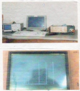
The execution of this program , we get this picture in OSC.
This program is display the name of the GOD on the OSC in Arabic
Languages ) الله )
148D:0100 MOV DX,0319
148D:0131 OUT DX,AL
148D:0103 MOV AL,25
148D:0132 DEC AL
148D:0105 OUT DX,AL
148D:0134 JNZ 0131
148D:0106 DEC DX
148D:0136 MOV AL, FF
148D:0107 MOV AL,80
148D:0138 INC DX
148D:0109 OUT DX,AL
148D:0139 OUT DX,AL
148D:011A DEC AL
148D:013A DEC DX
148D:010C JUZ 109
148D:013B MOV AL,FF
148D:010EMOVDX,0319
148D:013D OUT DX,AL
148D:0111 OUT DX,AL
148D:013E DEC AL
148D:0112 DEC DX
148D:0140 JUN 013D
148D:0113 MOV AL,80
148D:0142MOV DX,0318
148D:0115 OUT DX,AL
148D:0145 MOV AL,00
148D:0116 DEC AL
148D:0147 OUT DX,AL
148D:0118 JUZ 0115
148D:0148 INC DX
148D:011A MOV AL, 80
148D:0149 MOV AL,CO
148D:011C MOV DX,0319
148D:014B OUT DX,AL
148D:011F OUT DX,AL
148D:014C DEC AL
148D:0120 DEC DX
148D:014E JNZ 014B
148D:0121 MOV AL,FF
148D:0150 MOV DX,0318
148D:0123 OUT DX,AL
148D:0153 MOV AL,80
148D:0124 DEC AL
148D:0155 OUT DX,AL
148D:0126 JNZ 0123
148D:0156 INC DX
148D:0128 MOV AL,C0
148D:0157 MOV AL,25
148D:012A MOV DX,0319
148D:0159 OUT DX,AL
148D:012D OUT DX,AL
148D:015A DEC AL
148D:012E DEC DX
148D:015C JNZ 0159
148D:012F MOV AL,FF
148D:015E JMP 100
CONCLSION_
It is quite evident that we have had neglected the vital role of the immense development in the technology of computer especially in the industrial and other technolog-ical fields. In this days it becomes possible for the designers to connect the personal com-puters with some outside apparatus by means of integrating a suitable adapters which can be fixed in the expansion slot. The path way is of the type ISA. It is one of the adequate methods know to be used in connection and communication. A buff-ering system is accomplishable using 74LS244 chips and line drivers with three state output to provide a unidirectional buffering for sixteen computer lines to reach for an adequate assembly language which is needed to achieve the communication between the card and the processor inside computer.- It is found that the output of any ge-nerator used here is quite feasible to illustrate a different times by different stimulate. Those veritiedprocesses helped to reads for an assembly language generated by the automation ,ready to be used whenever it is needed as it is exhibited clearly in this paper. Finally, it is observed the the assembly language reached at by this research is quickly of which is hoped to be uitilized within the application verified programs. Moreover, this study is highly restricted to include some other advanced properties kn-owledge which can be the trends for future research in this field using three( x-y-z) dimension.
REFERNCES:-
1- Digital Control in Power Electronics,by Simone buso(2007) ,Khawll Naja
,Analog to Digtial Converters and Digital to Analog Converters(2006).
2-Operating System Concepts,by Silberschatz Galvin&Gagne(2005)
3-King Kuose and Rose.,Embeddedsystem Architecture. "A Comprehensive by
Tammy Noergraard"(2005)
4-Kurs and Rose and other(2005).
5-Broskcheor(2003),(2000)Comer,"Analog Circuit Design" ISBN/ASIN,(1990).see:extendability
6-Williams(2001),Wolf and Nut(2003-2004).
7-James Cook(1999),Computer Arhitecturer.
8-Skevens(1999),Tanenbaum(2001),Nult(2004),see each.
IJSER © 2012
http://www.ijser.org
International Journal of Scientific & Engineering Research, Volume 3, Issue 1, January-2012 4
ISSN 2229-5518
9-Luies C.E.(1997),The Connection of Personal Computer with Extenstion world for Measurement and Control Purposes.
10-W.S.Anglin and J.Lambek(1995),The Heritage of Thales.
11-Lortier(l989),Deitel(1990),Lortier(2003),see each of.
12- Wikipedia,Winfield Hi!land Paul Horowitz(l989),Logical Gate,Printed
Circuit Board
13- Thomas L.Floyd,3'd edition,Digtial Fundamentals.
14- Bill B. Bary,Small Computer And Theorm.
15- www.bizzybeemedia.com,Design Graphic Design.
1 6-New reports on the latest graphic hardware both Apple Macs and Windows .
17- System-In-Package Technology By Chistopher M. Scanlan and Nozad
Karim,Amkor technology,Inc.
18- (1966)Mealy
IJSER <b) 2012
http //www ijs er0rg