International Journal of Scientific & Engineering Research,Volume 3, Issue 6, June-2012 1
ISSN 2229-5518
Observation of the Nonlinear Behaviour of PFC Boost Converter and Control of Bifurcation
Arnab Ghosh, Abhisek Pal, Dr. Pradip Kumar Saha, Dr. Gautam Kumar Panda
Abstract— W ith rapid development in power semiconductor devices, the usage of power electronic systems has expanded to new and wide application range that include residential, commercial, aerospace and many others. However, their non -linear behavior puts a question mark on their high efficiency. This paper aims to develop a circuit for PFC boost converter to observe chaos and bifurcation diagrams. It is clear that the output storage capacitor is a main contributing parameter on the system stability, therefore, bifurcation maps are developed to determine the accurate minimum output capacitance valu e that assures the system stability under all operating conditions.
Index Terms— PFC boost converter; Phase Plane Trajectories ; Bifurcation diagrams ; Bifurcation Control .
—————————— ——————————
HE power electronic engineers observe some strange phe- nomena noise like oscillation. Actually power electronics system can exhibit a variety of nonlinear behaviours be- cause of periodic switching of the circuits. This kind of nonli- nearity is the main cause of harmonics generation i.e. degrada- tion of input power factor. In the last decade, bifurcation and chaotic phenomena have been reported in some type of DC- DC converters [1,5,8]. Here we are discussing about some non- linear phenomena of Power Factor Corrected (PFC) Boost
Converter.
The operation of the boost PFC converter [2, 6] has
been analyzed in details by many researchers. In practical circuits, it is much more difficult to arrange pure DC source, as well as the setup is much more expensive. So we are consi- dering rectified dc in spite of pure DC.
They linearised the system as their assumption. They as- sumed a very huge output capacitance (not acceptable in in- dustry) and it resulted in the time-invariant feedback signal that neglected the time-varying effect. Also, they replaced the input voltage with its root mean square (r.m.s.) value, neglect- ing the effect of its amplitude variation. Then, they intro- duced a small-signal equivalent circuit and the stability was
————————————————
![]() Abhisek Pal is currently pursuing M.Tech in Power Electronics and
Abhisek Pal is currently pursuing M.Tech in Power Electronics and
Drives at Jalpaiguri Govt. Engineering College ,India, PH-8900063865. E-mail: abhisekpal.ee @gmail.com
![]() Dr. Pradip Kumar Saha Ph.D., is Professor and Head of the Department of
Dr. Pradip Kumar Saha Ph.D., is Professor and Head of the Department of
Electrical Engineering at Jalpaiguri Govt. Engineering College, Jalpaiguri,
India, PH-9832443022.
E-mail: p_ksaha@rediffmail.com
![]() Dr. Gautam Kumar Panda Ph.D., is Professor of the Department of Elec- trical Engineering at Jalpaiguri Govt. Engineering College, Jalpaiguri, India, PH-9434449763.
Dr. Gautam Kumar Panda Ph.D., is Professor of the Department of Elec- trical Engineering at Jalpaiguri Govt. Engineering College, Jalpaiguri, India, PH-9434449763.
E-mail: g_panda@rediffmail.com
examined by this linear model .
The PFC converter is nonlinear system [6] due to a mul-
tiplier using and a large variation of duty cycle. There is also
present nonlinear term in its state equations. Here we will ob-
serve the chaotic behaviour and bifurcations of this converter.
What is Chaos?
The etymology of the word ―chaos‖[7,8] is a Greek word
―χα’ξ ‖ which means ―the nether abyss, or infinite darkness,‖ Namely, the god Chaos was the foundation of all creation. There is no standard definition of chaos. The chaos has some typical features: Nonlinearity, Determinism, Sensitive depen- dence on initial conditions, Aperiodicity.
What is Bifurcations?
The quantitative changes of system parameters can cause of
the qualitative changes of the system dynamics are called Bi-
furcations [7,8]. Naturally, bifurcations are very important
dynamical events that may affect the performance of engineer-
ing systems.
Modelling, simulation and circuit analysis are done by MAT- LAB respectively. These not only help in developing a deeper understanding of PFC converters but are also extremely im- portant tools for design verification and performance evalua- tion. These techniques help in the evaluation of a system with- out risking the huge cost and effort of developing and testing an actual converter.
Fig 1: Block Diagram of a boost PFC circuit
From the above Fig.1 the single phase sinusoidal voltage source vs is rectified by diode bridge and the rippled DC vol- tage vin is fed to the boost converter. The output voltage vo(ripple is presented as the value of the capacitor is taken
IJSER © 2012
International Journal of Scientific & Engineering Research,Volume 3, Issue 6, June-2012 2
ISSN 2229-5518
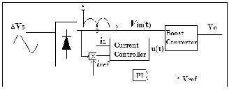
small) is obtained from load side. The output voltage vo is compared with a reference voltage (DC) vref. We use an integral controller to get steady state value of error signal. iref is obtained after combining the the result of controller, vin and inductor current (iL). Now iref or iL* is compared with iL. The duty cycle is maintained by the result of the comparator. The clock period and the value of the inductor are so chosen that the inductor current never falls to zero.
Fig. 2: Boost PFC ac-dc regulator under fixed-frequency Current Mode
Control.
Depending upon the block diagram we design the above model and derived the several expressions [2,3,4,6] which are given below.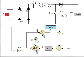
Supply system:
Under normal operating conditions the supply system can be modelled as a sinusoidal voltage source of amplitude vm and frequency fs. The instantaneous voltage is:
vs (t) = vm sin ωt (1)
where ω = 2pifs electrical radians/second and t is instanta-
neous time.
In some topologies, the input is rectified line voltage vd(t)
which can be given as:
vd (t) = |vs (t)| = |vm sin ωt| (2)
From the sensed supply voltage, an input-voltage template
u(t) is estimated for converter topologies with AC side induc-
tor as:
u(t) = vs (t)/ vm (3)
The input-voltage template for converter topologies with a
DC side inductor is obtained from:
u(t) = |vs (t)|/ vm (4)
Feedback controller:
PFC converters, like most power electronics systems, can-
not function without feedback control. Fig.1 shows a block
diagram of typical control scheme for PFC converters – the
current mode control [3]. This control scheme ensures regu-
lated DC output voltage at high input power factor. The out-
put DC voltage regulator generates a current command, which
is the amount of current required to regulate the output vol-
tage to its reference value. The output of the DC voltage regu-
lator is then multiplied with a template of input voltage to
generate an input current reference. This current reference has
the magnitude required to maintain the output DC voltage close to its reference value and has the shape and phase of the input voltage – an essential condition for high input power factor operation.
(i) Output voltage controller:
A proportional integral (PI) voltage controller is selected
for zero steady-state error in DC voltage (rippled in nature)
regulation. The output capacitor voltage vdc(or vo) is sensed and compared with the set reference voltage vref. The resulting voltage error ve(n) at the nth sampling instant is:
ve( n) = vref - vdc( n) (5)
The output of the PI voltage regulator vo(n) at the nth sampling instant of the PI
controller will be:
vo( n) = vo( n-1) + k p {ve( n) - ve( n-1)} + ki ve( n) (6)
Here kp and ki are the proportional and integral gain con- stants, respectively. ve(n-1) is the error at the (n - 1)th sampling instant. The output of the controller vo(n) after limiting to a
safe permissible value is taken as the amplitude of the input
current reference A (Fig. 2).
(ii) Reference current controller:
The input voltage template u(t) obtained from the sensed
supply voltage is multiplied by the amplitude of the input current reference A to generate a reference current. The instan- taneous value of the reference current is given as:
iL* = AB / C 2 (7)
where B is the input voltage template u(t) and C is the in-
put voltage feed forward component obtained by low-pass
filtering the sensed input voltage signal.
Semiconductor switches:
Semiconductor switches, Mosfet S and Diode D are
modelled as pure ON–OFF switches. No snubbers or non-
idealities in the switches are modelled.
Load:
The converters are modelled as resistive loads having
resistance R.
Power circuit:
The power circuit is modelled by first-order differen-
tial equations describing the circuit behaviour.
There are two states[1][5] of the circuit depending on whether
IJSER © 2012
International Journal of Scientific & Engineering Research,Volume 3, Issue 6, June-2012 3
ISSN 2229-5518
the controlled switch is open or closed. When switch is closed, the current through the inductor rises and any clock pulse arriving during that period is ignored. The switch opens when reaches the reference current. When switch is open, the cur- rent falls. The switch closes again upon the arrival of the next clock pulse.
The State Equations during “ON” period
diL/dt = Vin/L – ( ri * iL)/L (8)
dvc/dt = -vc/C(R + rc) (9)
The State Equations during “OFF” period
diL/dt = Vin/L – iL*(ri + R*rc/(R + rc))/L – vc*R/L(R + rc)
(10)
dvc/dt = (R*iL - vc)/C(R + rc) (11)
where,
Vin=Input Voltage
L = Inductor
C = Capacitor
iL = Inductor Current
vc = Capacitor Voltage,
ri & rc = Parasitic Elements
Simulation of PFC Boost Converter is done by MATLAB 7.8R2009a. The model is totally designed by SimPowerSystem and Si- mulink blocks [3,4].
C o n tin u o u s
PFC BOOST CONVERTER
p o we rg u i
Step
SW iL
iL vc
A + AC Volta ge Source
B -
+ive
-ive
vc
Vin
vc iL
OUTPUT
vc vs. iL Graph
BRIDGE RECTIFIER
BOOST CONVERTER
PW M vc
V in V ff
FEED FORW ORD CONTROLLER
PWM
iL*k iL A
V ff
V r e f
A
s ignal
Vref iL
6
CURRENT CONTROLLER
Subsystem
Fig. 3: Simulation of PFC Boost Converter
Here we are varying the value of Load Resistance R (in Fig.2) and we obtain the several periodic behavior of converter.
Case I(Period I Operation)
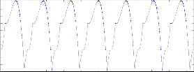
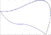
Vs=220sin ωt, L=40mH, C=100µF, R=40Ω, K1=400
280
260
240
220
200
180
160
140
120
100
42 44 46 48 50 52 54 56 58 60 62
Time (t)
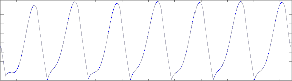
Fig.4(a) : O/P Voltage Waveform at Period I (R = 40 ohm)
9
8.5
8
7.5
7
6.5
6
5.5
5
4.5
4
42 44 46 48 50 52 54 56 58 60 62
Time
Fig.4(b) : Inductor Current Waveform at Period I (R = 40 ohm)
IJSER © 2012
International Journal of Scientific & Engineering Research,Volume 3, Issue 6, June-2012 4
ISSN 2229-5518
9
8.5
8
7.5
7
6.5
6
5.5
5
4.5
4
120 140 160 180 200 220 240 260
Capacitor Voltage (Vc)
Fig.4(c) : Phase Plane Trajectory(Case I)
260
240
220
200
180
160
140
Capacitor Voltage vs Inductor Current (Period I)
Case II(Period II Operation)
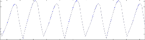
Vs=220sin ωt, L=40mH, C=100µF, R=44Ω, K1=400
8
7
6
5
4
120
42 44 46 48 50 52 54 56 58 60 62
Time (t)
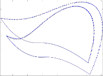
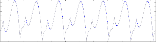
Fig.5(a): O/P Voltage Waveform at Period II (R = 44)
3
42 44 46 48 50 52 54 56 58 60 62
Time
Fig.5(b): Inductor Current Waveform at Period II (R = 44)
8
7
6
5
4
3
140 160 180 200 220 240 260
Capacitor Voltage (Vc)
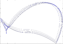
Fig.5(c) : Phase Plane Trajectory(Case II) Capacitor Voltage vs Inductor Current (Period II) Case III(Chaotic Mode Operation)
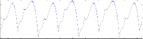
Vs=220sin ωt, L=40mH, C=100µF, R=65Ω, K1=400
240
230
220
210
200
190
180
170
160
42 44 46 48 50 52 54 56 58 60 62
Time (t)
6
5.5
5
4.5
4
3.5
3
2.5
2
42 44 46 48 50 52 54 56 58 60 62
Time
Fig.6(a): O/P Voltage Waveform at Chaotic Mode (R = 65)
Fig.6(b): Inductor Current Waveform at Chaotic Mode (R = 65)
6
5.5
5
4.5
4
3.5
3
2.5
2
160 170 180 190 200 210 220 230 240
Capacitor Voltage (Vc)
Fig.6(c) : Phase Plane Trajectory(Case III)
IJSER © 2012
International Journal of Scientific & Engineering Research,Volume 3, Issue 6, June-2012 5
ISSN 2229-5518
Capacitor Voltage vs Inductor Current (Chaotic Mode)
ANALYSIS OF EXPERIMENTAL RESULTS:
Here the state variables are inductor current (iL) and capacitor voltage (vc) .From above results we see that case I(Fig.4b) is operating at period I condition[7] and case II(Fig.5b) is oper- ating at period II condition[7]. The output voltage waveform in Fig.5(a) is much more ripple free than Fig.4(a). We get better result of output voltage at same value of inductor (L) and ca- pacitor (C), only changing the value of load resistance (R). The value of Capacitor(C) is chosen small just it operates as a boost converter. If we can increase more values of load resis- tance R, the system will operate at chaotic region and we can get better ripple free output voltage. This is the main observa-
tion that we get better output voltage profile at least value of capacitor. So, the investment is much more less than other conventional practical instruments.
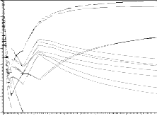
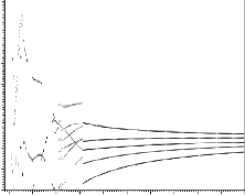
Bifurcation diagrams are obtained from FORTRAN and ORIGIN 5.0 software. The data files are obtained after execut- ing the FORTRAN programme of State Equations (8), (9), (10), (11) of PFC Boost Converter and iref equ (7). This data files are plotted by ORIGIN 5.0. Results are given below in Fig. 7(a), (b), (c), (d).
35
30
25
20
15
10
5
0
0 100 200 300 400 500 600 700 800 900 1000
RESISTANCE (OHM)
900
800
700
600
500
400
300
200
100
0 100 200 300 400 500 600 700 800 900 1000
RESISTANCE (OMH)
Fig.7(a):R vs iL (R is varied 1 to 1000ohm with step of 0.5)
Fig.7(b):R vs Peak_ vc (R is varied 1 to 1000ohm with step of 0.5)
45
40
35
30
25
20
15
10
5
0
0 10 20 30 40 50 60 70 80 90 100
INDUCTANCE (mH)
550
500
450
400
350
300
250
200
150
100
50
0
0 10 20 30 40 50 60 70 80 90 100
INDUCTANCE (mH)
Fig.7(c):L vs iL (L is varied 1 to 100mH with step of 0.5)
Fig.7(d):L vs Peak_ vc (L is varied 1 to 100mH with step of 0.5)
Analysis of Bifurcation Diagrams:
The above bifurcation diagrams are much more differ from other conventional bifurcation diagrams. In caonventional process the border [8] is fixed i.e. Iref (or iL ) is constant. In our experiment Iref (or iL*) is time varying natute i.e. order is time- varient. It is very difficult to analysis the bifurcation diagram properly. Actually the bifurcation is Period Doblling [7,6] in nature. The analysis is not given here. We are now working on analysis of diagrams.
principle of control of bifurcations is based on perturbation or control by adding an extra input to the nonlinear dynamical system with the aim to modify its dynamics by stabilizing the desired behaviour. In our system, an extra Time Delayed Feedback action can be placed at any point of the voltage loop, for instance, at the output of the voltage controller.
IJSER © 2012
International Journal of Scientific & Engineering Research,Volume 3, Issue 6, June-2012 6
ISSN 2229-5518
340
320
Bifurcation Diagram g vs PEAK Capacitor Voltage
300
280
260
240
220
200
180
160
140
0.1 0.2 0.3 0.4 0.5 0.6 0.7 0.8 0.9
Gain of Time Constant
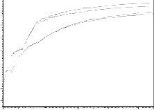
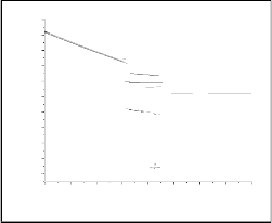
Fig.8:gtdf vs Peak vc (gtdf is varied 0.1 to 0.9 with step of 0.01)
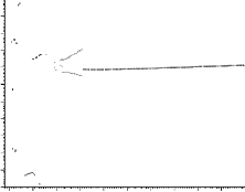
260 Bifurcation Diagram R vs Vc
240
220
200
300
250
Bifurcation Diagram R vs PEAK Vc
180
160
200
140
120
150
100
80
100
60
40
0 200 400 600 800 1000
Resistance
50
0 200 400 600 800 1000
Resistance
Fig. 9(a):R vs vc (R is varied 1 to 1000 with step of 0.5)
gtdf = 0.9

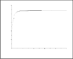
Fig.9(b):R vs Peak vc (R is varied 1 to 1000 with step of 0.5)
gtdf = 0.9
From above figure (Fig. 8) we see that the stable value of vc will be got after the value of gtdf = 0.6. So, we assume the value of gtdf = 0.9 and obtain the new bifurcation diagrams.
The boost PFC converter with continuous current mode control has been examined. Results highlight that the pro- posed model of practical pfc converter, experimental results and bifurcation diagrams. The value of load resistance is in- creased; the output capacitor voltage waveform is going to period I to period II and chaotic mode, that is the main cause of bifurcation. But the main benefit is the output voltage ripple is going less than the previous. Then the bifurcation control is implemented for obtaining stable operating zone. In a DC/DC converter system, the input voltage is constant and therefore the dynamical behavior is periodic with the switching frequency . On the other hand, the input voltage of the boost AC/DC PFC converter system is periodic with the line frequency. The results highlight that the dynami- cal behavior is periodic with the line frequency not with the switching frequency and simulation results are also agree with our statements.
If the Fig.7(b) will be compaired with Fig. 9(b), it will be shown the 2nd Fig. more stabler than 1st. It is possible only changing the bifurcation parameter i.e. bifurcation control.
The authors wish to thank Dr. Soumitra Banerjee of the Indian Institute of Science Education and Research, Kolkata for his helpful suggestions in improving the paper.
[1] Soumitro Banerjee and Krishnendu Chakrabarty, ―Nonlinear Modeling and Bifurcations in the Boost Converter‖ in IEEE TRANSACTIONS ON POWER ELECTRONICS, VOL. 13, NO. 2, MARCH 1998.
[2] Ashish Pandey, Dwarka P. Kothari, Ashok K. Mukerjee and Bhim
Singh, ―Modelling and simulation of power factor corrected AC–DC converters‖ in International Journal of Electrical Engineering Educa- tion.
[3] Arnab Ghosh, Abhisek Pal, Dr. Pradip Kumar Saha and Dr. Gautam Kumar Panda, ―Study The Nonlinear Behaviour of PFC Boost Co n- verter‖ in IEM International Journal of Management & Technology, Vol. 2, No. 1, ISSN No.: 2296-6611, January 2012.
[4] Arnab Ghosh, Abhisek Pal, Dr. Pradip Kumar Saha and Dr. Gautam
Kumar Panda, ―Study The Nonlinear Behaviour of PFC Boost Co n-
IJSER © 2012
International Journal of Scientific & Engineering Research,Volume 3, Issue 6, June-2012 7
ISSN 2229-5518
verter‖ in 2nd Annual International Conference IEMCON 2012, pp. 137-141, IEEE Calcutta Chapter, January 2012.
[5] Ammar Nimer Natsheh, ―ANALYSIS, SIMULATION AND CO N- TROL OF CHAOTIC BEHAVIOUR IN POWER ELECTRONIC CONVERTERS‖ in Doctoral Thesis Submitted in partial fulfilment of the requirements for the award of the degree of Doctor of Philosophy of Loughborough University.
[6] Yi-Jing Ke, Yu-Fei Zhou and Jun-Ning Chen, ―Control Bifurcation in
PFC Boost Converter under Peak Current-Mode Control‖ in IPEMC
2006.
[7] Soumitro Banerjee, ―Dynamics for Engineers‖ (John Wiley & Sons Ltd, The Atrium, Southern Gate, Chichester, West Sussex PO19 8SQ, England).
[8] Soumitro Banerjee and George C. Verghese, ―NONLINEAR PH E- NOMENA IN POWER ELECTRONICS‖(Published by John Wiley & Sons, Hoboken, NJ).
[9] Arnab Ghosh, Abhisek Pal, Dr. Pradip Kumar Saha and Dr. Gautam Ku-
mar Panda, ―Observation The Nonlinear Behaviour of PFC Boost Conver-
ter and Control of Bifurcation‖ in INTERNATIONAL CONFERENCE ON
EMERGING TRENDS (ICET 2012), NIT Durgapur, March 2012, IEEE Stu- dent’s Branch.
[10] Arnab Ghosh, Abhisek Pal, Dr. Pradip Kumar Saha and Dr. Gautam Ku-
mar Panda, ―Exploration of Bifurcation and Chaos in PFC Boost Conver- ter‖ in National Conference on Recent Trends in Electrical, Electronics and Embedded Systems, RTEEE - 2012, March 2012, Chennai.
[11] Arnab Ghosh, Abhisek Pal, Dr. Pradip Kumar Saha and Dr. Gautam Ku- mar Panda, ―Observation The Chaos and Bifurcation Diagrams of CCM PFC Boost Converter‖ in National Conference on Pervasive Computing and Communications, NCPCC - 2012, pp. 220 - 225, March 2012, Kolkata.
[12] Arnab Ghosh, Abhisek Pal, Dr. Pradip Kumar Saha and Dr. Gautam Ku-
mar Panda, ―Exploration of Bifurcation and Bifurcation Control of PFC Boost Converter‖ in 4th National Conference on Innovation in Power Elec- tronics Controls and Systems, IPECS - 2012, March 2012, Trichy.
IJSER © 2012