International Journal of Scientific & Engineering Research, Volume 6, Issue 1, January-2015 1233
ISSN 2229-5518
Negative-differential resistance effect in ternary chalcogenide
semiconductorInGaTe2
A.T. Nagat.1, J. A.M.Abdulwahed2, S. R. Alharbi1, E. M. Saed3 and H. I. El-Saeedy4
1-Physics Department, Faculty of Sciences for Girls, King Abdulaziz University, KSA
2- Physics Department, Umm-AlQura University-College in Qunfudah-female- KSA
3- Physics Department, Faculty of Sciences, South Valley University, Qena, Egypt
4- Physics Department, Faculty of Sciences for Girls, King Khalid University KSA
jazi1430@windowslive.com
Abstract: Indium Gallium ditelluride single crystal, were prepared by a special high efficiency, low cost, design constructed locally, based on Bridgman technique. A special Perspex sample holder and quartz cryostat were used to investigate the switching phenomena in InGaTe2 single crystal. Current-controlled negative resistance (CCNR)has been observed for the first time. The switching effect observed in such crystal shows memory. The CVC of the compound show two different regions: an ohmic region at low-current densities and a negative differential resistance (NDR) region at higher current densities. This behavior has been explained by an electrothermal model. The results strongly indicate that the phenomenon in our samples are sensitive to temperature, light intensity and sample thickness as well. Switching parameters (Ith,Vth, Ih, Eth, Pth and ROFF/RON) are found to depend on the surrounding conditions as well as sample thickness.
Keywords: Indium gallium ditelluride, CCNR, memory, switching, NRD region, S-shape.
—————————— ——————————
1. Introduction
The switching phenomenon one of the numerous interesting effects arising in strong electric field(1). The phenomenon has been observed in a great number of crystalline, amorphous and liquid semiconductor. Electrical threshold switching and memory in semiconductors have a roused great interest in recent years. Among the materials in which these effects take place there are chalcogenides(2). AIIIBIIIC 2 VIsemiconducting ternary chalcogenides form a layered-chain structure as AIIICVI-BIIICVI in which the compounds AIIICVI and BIIICVI have the ratio 1:1. For instance in the compound InGaTe2 , which is a ternary material from this class, the compounds are arranged in the form InTe-GaTe. Although the ternary semiconducting chalcogenides have been investigated extensively in recent years, very few investigation have been performed on InGaTe2 . The crystal structure of this compound is reported(3) some information about the electrical and Hall coefficient was published(4,5), and also the optical properties was investigated(6). Binary AIIIBVI and ternary AIIIBIIIC2 VI compounds exhibit many non-linear effects in electrical behavior, such as S-shaped characteristic in the negative differential resistance region (NDR), switching and memory effects, polarization and depolarization effects(7). The switching phenomenon has been known for more than thirty years and has been investigated by many authors. Today, it still remains a subject of contradiction and mystery. Therefore, all investigations leading to its
clarification are beneficial. Negative differential resistance (NDR) and electrical switching effects attracted the interest of many researchers. This is due to possible technologicalapplications, such as switching and memory devices, oscillators, thermistors, etc. The InGaTe2 compound just like other ternary semiconductors compounds could have many possible applications ranging from use in solar cells to nonlinear effects such as S-type characteristics with voltage oscillations in the negative resistance region andmemory switching effects. In view of the absence of published observations of these phenomena in this compounds, the authors under took such work and report here the results of switching effects and some factors affecting it. A lot of work has been done to establish the mechanisms of switching process, but at present, there still exists uncertainty about the actual physical content of these theories. Since then, the characterization and utilization of this negative-resistance behavior has received considerable attention. The absence of data on the characteristics of switching about the compound InGaTe2 makes it difficult to estimate potential application of this material in electronic device technology.
2. Experimental details
IJSER © 2015 http://www.ijser.org
International Journal of Scientific & Engineering Research, Volume 6, Issue 1, January-2015 1234
ISSN 2229-5518
2.1 Apparatus and method of crystal growth.
Single crystals of InGaTe2 were grown from melt using a modified Bridgman technique in a special design constructed locally. InGaTe2 crystals were prepared in bulk form by direct fusion of stoichiometric amount of the constituent elements In, Ga and Te (purity 99.9999%) in an evacuated seald silica tube (10-5Torr).
The silica tube has a trapped tip at the bottom to facilitate seeding in the growth process. The quartz ampoule was coated internally with a thin layer of pyrocarbon to prevent the produced ingots from adhesion with silica
tube. At the beginning of the growth run, the ampoule was held in the hot zone of the furnace at 1050K for 10h for melt homogenization. Then the melt shaken during heating several times to accelerate the diffusion of the contaminates through each other. After this the ampoule was moved into the middle temperature zone of the furnace with a temperature of 970K according to the phase diagram(8) at rate 2.3mm/h. Afterward, the ampoule was cooled down slowly in the third zone of the furnace. Details of the experimental equipment for crystal growth and of the preparation procedures are described elsware(9). After the product had cooled to room temperature, the crystal was characterized by X-ray diffraction analysis and DTA. To assure the presence of the crystalline phase with high quality in the prepared ingot with black metallic luster. The time required for this process was about 17 days.
2.2 Design and constructed of the sample holder and cryostat
To study the switching phenomenon of bulk specimen, the sample was prepared in a rectangular shape and placed in a point contact holder. The specimen holder consists of two flat copper sheets fixed on a rectangular block of insulating material (Perspex). A brass screw fixed in the midpoint of the copper sheet faces, acts as point electrodes, the brass screw can be moved gently to make light pressure-contact on the specimen. The sample with its holder was positioned in a special system to allow temperature control in the investigated range. More details of the sample holder were described early(10). The system was attached to a vacuum pump giving the possibility of measurements under vacuum. The environment temperature of specimen under test was measured by means of a calibrated spot-welded chromel-Alumel thermocouple. The investigation was carried out in wide range oftemperature in order to show the influence of an ambient temperature on switching behaviour. Silver paste was applied on the opposite parallel surfaces of the sample. In order to investigate the effect of light intensity on the switching phenomena at room temperature, sample with appropriate thickness are mounted in a cryostat equipped made of quartz glass with suitable flat portion and clamped in its holder provided with apertures to allow the passage of radiation. The sample was illuminated at normal incidence. Details of the apparatus and cryostat described in ref.(11)
2.3Theexperimental arrangement and measuring technique
In this work, the samples are symmetric sandwich type structure in which single crystal samples of rectangular shape were prepared with smooth and mirror like surface are placed between two metal electrodes. We used a simple circuit consisted of a digital DC stabilized programmable power supply Thermo EC Type, with accuracy better than ±1% of set value, digital Keithleyelectrometer 617, sample and load resistance were connected in series, the sample was connected in parallel to a sensitive voltmeter for measuring the potential difference across its ends. For tracing the I-V curves the power supply voltage was increased gradually and slowly. The values of the current and potential difference across the sample were recorded when the bias was increased until a threshold value of the electric field (~1.42V/cm) was reached, switching from the high to the low-resistivity state took place in the crystal. After which the series resistor, limited the applied voltage for preventing crystal destruction. The current passing through the sample can be easily reversed or cut-off by applying three-pole doubles stage reversing switch. The investigation was carried out in the temperature range
120K to 300K in order to show the influence of ambient temperature on the switching behaviour. The temperature of the specimen was maintained constant during each measurement. Also the high and low resistivity states were sensitive to the light intensity and sample thickness. To study the effect of light intensity, white light was focused on the surface of the sample. The intensity of the radiation was measured with a luxmeter (Fisher Scientific mark) from 0 to 1500 Lux. Samples with thickness varying from (0.1-0.2cm) were used to investigate the influence of the sample thickness on the switching characteristics. Details of the experimental procedures and apparatus were published earlier(12).
3. Results and Discussion
3.1General description of the switching phenomena
IJSER © 2015 http://www.ijser.org
International Journal of Scientific & Engineering Research, Volume 6, Issue 1, January-2015 1235
ISSN 2229-5518
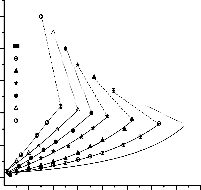
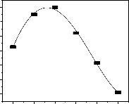
The room temperature I-V characteristics for the bulkInGaTe2 semiconductor crystal are shown in fig.1. The behavioris typical I-V characteristics ofCCNR,similar to many chalcogenide materials(13-15). The current passing through the specimen increases with increasing voltage up to certain value, called "threshold voltage". After that voltage, the I-V characteristics moves from the high-resistance state (OFF state) to the low-resistance state (ON state). To study the features of various parts of the I-V curve. At low voltages (0≤V≤Vth ) thecharacteristic exhibits ohmic behavior from which the resistance of the specimen can be determined. At critical value of the
applied voltage Vth the current increases suddenly with decreasing the voltage across the specimen, which means that a negative resistance occurs , therefore, the I-V characteristic could be classified as characteristics of

negative resistance devices. A sudden increase in current and drop in voltage was observed in a very short time of the order of 10-9sec i.e., electrical switching takes place, data cannot be taken in this region.
100
80
60
40
20
0
-25 -20 -15 -10 -5 0 5 10 15 20 25
-20
-40
-60
-80
-100
Vx10 (volt)
Fig. 1. I-V characteristic for InGaTe2 single crystal.
After the negative differential resistance region, the sample stays in the low-resistance state even the applied voltage is reduced to zero. This state is a conductive one. This is because the conductivity becomes about two orders of magnitude higher than in the OFF state.The above features indicate that the switching process is of memory type. At present, we have no information regarding these changes, but we believe that the memory switching effect in these compounds occurs as a result of two consecutive processes, an electric process give rise to the negative resistance (Lampert's effect) and a Joule effect in the localized zones, which gives rise to the memory effect. This leads to the conclusion that the favorable mechanism of switching in the present study may be the electrothermal mechanism. Fig 1 shows the forward and reverse biased I-V characteristics of InGaTe2 single crystals. The general behavior of the CVC is the same for both polarities, indicating that it is symmetric with respect to the polarity of the applied field with two distinct regions. The OFF-state and the negative- differential resistivity (NRD) regions. We can also observe that the InGaTe2 is a ternary chalcogenide semiconductor exhibiting S-shape I-V characteristic.
3.2 Temperature dependence of the I-V characteristic.
The temperature dependence of the I-V characteristics is an important factor to define a switching material for technological applications. In other word choosing a switching material for an information storage application depends on the variation of switching properties on temperature. In the present study the effect of the temperature on switching behavior has been investigated in a wide temperature range extend from 120K to
300K. the temperature dependence of the I-V characteristic curves of Ag-InGaTe2 -Ag structures under static conditions are shown in fig 2.It is clear from this figure that cooling increased the threshold switching voltage and lowered the threshold current. It is obvious that Vth decreases with increasing the temperature in accordance with the previous observations obtained by other authors(16-18) for other compounds, while Ith increases with increasing the temperature. The part of the I-V characteristic exhibiting, negative slope is usually NDR. Its width, slope, threshold voltage and threshold current, as well as holding voltage and holding current are the main characteristic features of this region. In the holding branch therefore the electrothermal balance between Joule's heat, produced in the bulk and heat flux into the electrodes seems to play an essential role for sustaining the high current density, with decreasing ambient temperature the critical voltage Vth at which the slope dI/dV
first become negative shifts to higher voltage values, while the corresponding current (threshold current) shifts
to lower current values. The holding voltage Vh increase with decreasing temperature, while the holding current increases with increasing temperature. It is clear from the curves the current-voltage characteristics for InGaTe2 single crystal has a characteristic S-shape as shown schematically in the figure for the entire temperature range under investigation. The switching and threshold voltage can be understood in terms of the following electrothermal model(19,20) for the pre-switching region. The temperature of the semiconductor is raised due to
IJSER © 2015 http://www.ijser.org
International Journal of Scientific & Engineering Research, Volume 6, Issue 1, January-2015 1236
ISSN 2229-5518
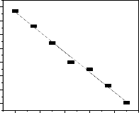
Joule-heating. Since the conduction process in the material is thermally activated, the conductivity of the sample will increase when it is heating, this will allow more current to flow through the heated regions and allow more Joule heating, resulting in a further increase in the current density.Ultimately the temperature rise will become sufficient to initiate a thermal breakdown owing to the strong temperature dependence of the conductivity. As can be seen from the experimental plot of fig 2a and also predicated by the electrothermal model, the temperature is greatly influences both the form of the I-V curves and the threshold voltage Vth (i.e, the appearance of the NDR region of the I-V characteristics is weaker at lower temperatures). According to these comments, the threshold current decreases with increasing the threshold voltage. It is easily seen that the I-V curves depend strongly on the ambient temperature of the investigated specimen. From these curves one can plot the variation of the threshold voltage Vth and the threshold current Ith with the ambient temperature as shown in fig 2b. Increasing the ambient temperature of the InGaTe2 specimen, increases the threshold current, while it decreases the threshold voltage (the two relations are linear). This indicates that an electrothermal mechanism is involved in the switching process.
(a)
100
80
60
40
20
120 K
150 K
180 K
210 K
240 K
270 K
300 K
80
(b)
60
40
20

Vth 44
i th
40
36
32
0
10 20 30 40 50 60 70 80
V × 10 (volt)
120 160 200 240 280 320
T K
Fig. 2. a. The temperature dependence of switching effect for InGaTe2 single crystal. b. The dependence of Vth and
Ith on ambient remperature for InGaTe2 compound
This behavior may be attributed to the fact that the rate of recombination is greater than the rate of thermal generation of free charge carriers, another possible contributing factor may be the effect of trapping centers which leads to smaller values of the threshold current as the temperature decreases. The relation between the threshold voltage and the ambient temperature can be described by an Arrhenian formula(21)
V = V
exp − =∆E
th 0
kT
Where V0 is constant and ΔE is the activation energy for switching and k is theBoltzman constant. Therefore, plotting lnVth versus 103/T for the studied InGaTe2 semiconductor compound yields linear relations as shown in fig 3a. This relation satisfying the above equation. The dependence of Vth on T was analyzed on the basis the thermal-field Frenkel effect. The relation between Vth and T is described by the following expression(16)
π=ε ε
Vth =
0 ∞ d (φ − CT )2
e
IJSER © 2015 http://www.ijser.org
International Journal of Scientific & Engineering Research, Volume 6, Issue 1, January-2015 1237
ISSN 2229-5518
(a)
6.6
6.4
6.2
6.0
5.8
5.6
5.4

3 4 5 6 7 8 9
10 3 / T ( K-1 )
(b) 28
26
24
22
20
18
16
14
120 160 200 240 280 320
T (K)
Fig. 3. a. The dependence of lnVth against 1000/T for InGaTe2 compound, b. The dependence of (Vth )1/2against T for ternary chalcogenide InGaTe2 single crystal.
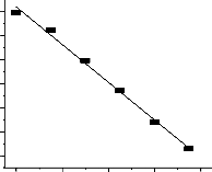
Where ε0 is the permittivity of vacuum, ε∞ is the electron component of the permittivity, d is the distance between two electrodes, C is a constant, e is the electron charge, ϕ is the depth of the potential well and T is the absolute temperature. The variation of Vth with temperature is plotted in fig 3b using the coordinates (Vth )1/2 and T. Clearly, within limits of exponential error, the results fit a straight line. This demonstrates that the switching in M-InGaTe2 -M structures from a high- to low- resistivity state occurs under the simultaneous action of the electric potential and temperature(22).This claim must be supported by the dependence of the threshold field on the thickness of the active region. The power dissipated (Pth= Vth× Ith) was calculated for the investigated
sample. The power necessary to change the material from the high resistance state to the low-resistance state is called the threshold power Pth. The threshold power is also depends on the ambient temperature. Calculation indicated that the magnitude of Pth decreases as the temperature increases as shown in fig 3b. This led us to the assumption that as temperature increases the number of random collisions as well as scattering between the charge carriers, the rate of thermal generation of free charge carriers smaller than the rate of recombination and the effect of trapping centers increases as the temperature increases.
All these factors led to the decrease of the threshold power as the temperature increases. So this result is quite logical, since the power necessary for initiate switching decreases with temperature increase as shown in fig
4a.The effect of the surrounding temperature on the sample resistance ratio was also determined. The OFF and
ON state resistance ratio (ROFF /RON ) depends on temperature which increase as temperature increase as seen in fig 4b. The resistance ratio at room temperature is of the order of 3.48.
(a)
24
22
20
18
16
14
12
10
120 160 200 240 280 320
T (K)
(b) 3.6
3.2
2.8
2.4
2.0
1.6
120 160 200 240 280 320
T (K)
Fig. 4 a. The variation of threshold power with temperature for InGaTe2 compound. b. The dependence of the ratio
ROFF /RON against T for InGaTe2 compound.
3.3 Influence of light intensity on the switching effect.
IJSER © 2015 http://www.ijser.org
International Journal of Scientific & Engineering Research, Volume 6, Issue 1, January-2015 1238
ISSN 2229-5518
The effect of light intensity on CVC is represented in fig 5a, which show that I-V characteristics of InGaTe2 at room temperature for different illumination doses (0,300,600,900,1200,1500 Lux). As observed from the curves in the figure, the behaviour of the CVC has the general form of switching with S-shape.
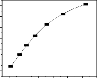
We notice that a sharp rise in the illumination intensity leads to a quick transition from the high-resistivity state tolow-resistivity state because thefield necessary for switching is reached quickly as the light intensity increases.It is evident from the I-V characteristics as a whole are shifted towards lower potentials with an increase in the intensity of the incident light. Additionally, we can see that the form of the CVC and the magnitude of the photo-current depend strongly on the intensity of the incident light.This means that in the case of weak illumination, the threshold voltage is larger and the threshold current value is smaller than the values obtained in the case of intense light. Additionally, we can observe a marked increase in the holding current Ih as the light intensity increases, which the holding voltage gradually increases with a decrease in the illumination doses. Fig. 5b illustrates the dependence of Vth and Ith on the light intensity. As can be seen from the figure, the threshold voltage decreases linearly with increasing light intensity, whereas the threshold current increases also linearly with increasing illumination. This indicates that as the light intensity increases, the number of charge carriers generated by photons increases leading to a growth of the current as the light dose increases. The main contribution comes from photo-carrier generation through excitation states is larger than recombination process. The relation between the threshold power Pth with light intensity is presented graphically in fig.5c. In general, the threshold power decreases linearly with light intensity. This may be due to photogeneration processes which take place under illumination of the sample and lead to low power for switching as the intensity dose increases. The dependence of the resistance ratio ROFF /RON on the illumination intensity was also determined.
(a) 120
100
80
60
40
20
0
 dark
dark
300 Lux
600 Lux
900 Lux
1200 Lux
1500 Lux
5 10 15 20 25 30 35 40 45
V × 10 ( Vo l t )
(b) 50
40
30
20
10
0

75
Vth
i th 70
65
60
55
50
0 400 800 1200 1600
I ( L u x )
(c) 20
19
18
17
16
15
14
0 400 800 1200 1600
I ( Lux )
Figure5. a. Current-voltage curves at different values of light intensity. b. The dependence of Vth and Ith . c. The dependence of threshold power for InGaTe2.
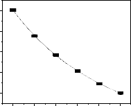
ROFF /RON increases gradually as the light intensity increases in the low intensity region, while it increases rapidly with light illumination in the high intensity region as seen in fig. 6. The ratio ROFF /RON at room temperature as calculated is 1.7 at zero-Lux and increases as the light intensity increases becoming 6.15 at 1500
Lux.
IJSER © 2015 http://www.ijser.org
International Journal of Scientific & Engineering Research, Volume 6, Issue 1, January-2015 1239
ISSN 2229-5518
7
6
5
4
3
2
1
0 400 800 1200 1600
I (L u x)
Figure 6. The dependence of the ratio ROFF /RON against light intensity for InGaTe2 compound.
3.4 Thickness dependence of switching effect.
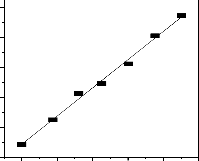
The identification of the specimen whose resistances are changed from a high value in the OFF-state to a very low value in the ON-state by the lowest switching power can be achieved through the study of the effect of the specimen thickness on the switching behavior. The overall features of the I-V characteristics of InGaTe2 are altered by changes in the sample thickness. Room temperature I-V characteristics for the investigated compound were studied for samples of thickness between 2 mm and 1 mm. Fig. 7a represents the dependence of the switching behavior on the thickness of InGaTe2 specimen. The graph indicates that the threshold potential changes with the specimen thickness, the widths of the dashed lines which represents the variation from the OFF-state to the ON-state, decrease with increasing sample thickness. The observed results indicates that the switching can be easily controlled by controlling the sample thickness. The holding current is thickness dependent, also the holding voltage is affected by the active thickness of the specimen, i.e., it decreases as sample thickness increases, while the holding current increases as the sample thickness increases. Investigation of the effect of sample thickness on switching phenomena is useful for a chosen specimen whose resistance is to change from high value (OFF state) to a very low (ON state) by lowest switching power. Fig 7b shows the effect of sample thickness on switching phenomena parameters of p-type InGaTe2 at room temperature . The curves indicate that the threshold potential and current change with the thickness of the active region. It is clear from the curves in fig 6b that the threshold voltage decreases rapidly and linearly with increasing sample thickness, while the threshold current increases rapidly and linearly with sample thickness. One may conclude that an increase of the specimen thickness lowers the potential for switching process in a specimen under test. Fig. 7c shows the dependence of the threshold field on the thickness of the sample. It is clear that Eth decreases with increasing sample thickness. This indicates that the electric field has a profound influence on the ability of the samples to undergo transits from the OFF state to an effective region of negative differential resistivity. This evident influence of the electric field supports the suggestion that the switching mechanism in InGaTe2 samples
may involve both electronic and thermal processes(23).

(a) 140 0.1 cm
120
100
80
60
40
20
0
0.12 cm
0.14 cm
0.16 cm
0.18 cm
0.2 cm
5 10 15 20 25 30
V × 10 (v o l t)
(b) 30
25
20
15
10
5

th 80
i th
70
60
50
40
0.10 0.12 0.14 0.16 0.18 0.20
d ( cm )
IJSER © 2015 http://www.ijser.org
International Journal of Scientific & Engineering Research, Volume 6, Issue 1, January-2015 1240
ISSN 2229-5518
(c)
2.5
2.0
1.5
1.0
0.5
0.10 0.12 0.14 0.16 0.18 0.20
d ( c m )
Figure7. a. I- V characteristics with various thickness. b. The dependence of V th and Ith against sample thickness, c. The dependence of Eth against sample thickness for InGaTe2 compound.
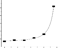
The variation of the threshold power Pth with the sample thickness is plotted in fig. 8a. It can be seen that the threshold power increases exponentially as the thickness increases reaching its highest value at 1.4mm, after which Pth decreases.This indicate that there is a critical value of the thickness of the active region at which the power necessary for switching decreases as the thickness of the sample increases. Thus, we can see that the switching can be easily controlled by controlling the specimen thickness. The resistance ratio varies from 2.1 to
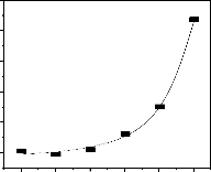
10.7 in the sample thickness range investigated in this study. At the beginning increasing the thickness leads to slowly increases in the ratio up to 1.6mm thickness, after which increases rapidly with thickness, this behavior is plotted in fig. 8b.
(a) 14
13
12
11
10
9
8
0.10 0.12 0.14 0.16 0.18 0.20
d ( c m )
(b) 12
10
8
6
4
2
0.10 0.12 0.14 0.16 0.18 0.20
d ( c m )
Figure8. The variation of the threshold power Pth (a) and the ratio ROFF /RON (b) for InGaTe2 compound.
4. Conclusion
For the purpose of investigation the possibility of the practical application of the switching effect with memory of InGaTe2 , we have grown and studied single crystals of this material.
This investigation is necessary to show the sensitivity of the switching phenomenon to the surrounding
conditions, that is a good mentor for the possibility of the test material as switching elements in electronic devices. The major features of the switching phenomena in InGaTe2 ternary chalcogenide semiconductor crystals can be summarized as follows:
1- First observations of the switching process in InGaTe2 ternarychalcogenidesemiconductor crystals are reported.
2- It is found that indium gallium ditelluride single crystals exhibit bistable operations or memory switching.
3- In the CVC for InGaTe2 Current-Controlled Negative Resistance (CCND) is reported for the first time.
4- The current-voltage characteristics are symmetrical with respect to the polarity of the applied voltage and
current.
5- The form of the CVC is of S-shape type from the common form of the switching phenomena.
IJSER © 2015 http://www.ijser.org
International Journal of Scientific & Engineering Research, Volume 6, Issue 1, January-2015 1241
ISSN 2229-5518
6- When the applied voltage exceeds a threshold voltage, the unit switches along the load line to the conducted state. The critical field for switching inInGaTe2 is 1.42V/cm at room temperature.
7- The results strongly indicate that the switching phenomena observed in our samples are very sensitive to
temperature, light intensity and sample thickness. The switching parameters also are checked under the influence of various ambient conditions.
8- In view of these properties, our material can be used as switching elements and memory elements in electronic devices.
5.References
[1] Yahia, I. S., Faden M., Sakz G. B. and Shenouda S. S.,"Memory switching of ZnGa2Se2 thin films as a new material for phase change memories (PCMS)"J. Alloy. And Comp. 507 (2010) 551-556
[2] Al-Orainy R. H. and Nagat A. T., " Preparation and switching behaviour characterization of some quaternary Thallium chalcogenide compounds" Acta Phys. Pol. A 123 (2013) 14-25
[3] Deiserth, H. J., Muller D. and Hahn H. "structure investigation in InGaSe2 and InGaTe2" Z. Anorg. All.
Chem. 525 (1985) 163-172
[4] Mobarak M., Berger H., Lorusso G. F., Capozzi V., Perna G., Ibrahim M. M., Margaritondo G. "The growth and properties of single crystal GaInTe2 a ternary chalcogenide semiconductor" J. Phys. D-Appl. Phys. 31 (1998) 1433
[5] AlOrainy R. H., Nagat A. T., Bahabri F. S., Saed E. M and El-saady H. I. "Experimental investigation of electrical conductivity and Hall effect in GaInTe2 single crystals" Australian J.Basic and Applied Sciences
6 (2012) 323-328
[6] Salaev E. Yu. andSafarov N. Yu "long-wave IR reflection spectra of InGaTe2" physics of semiconductors in Russian lang 8 (1981) 29-31
[7] Abay B., Gurbulak B., Yilderum M.,Efeoǧlu H. And Yoǧurtçu Y. K. "Electrothermal investigation of the switching phenomena in p-type TlInSe2 single crystals" Phys. Stat. Sol. A 153 (1996) 145-151
[8] Blachnik R. and Klose e. "Experimental investigation and thermodynamic calculation of excess enthalpies
in Ga-In-Te system" J. Alloy. And comp. 305 (2000) 144
[9] Hussein S. A. and Nagat A. T., (On the preparation and electrical properties of thallium selenidemonocrystals), Cryst. Res. Technol 24 (1989) 283-289
[10] Nagat A. T., Hussein S. A., Gameel Y. H. AndGamal G. A. " Switching effect with memory in Thallium sulphide single crystals" Phys. Stat. Sol. (a) 121 (1990) 201-205
[11] Al-Ghamdi A. A., Hussein S. A. and Nassary M. M."Memory switching effect in GaSe single crystals" Mat. Sci. Res. India 2 (2004) 107
[12] Hussein S. A. "Memory switching effect in single crystals of Thallium selenide" Cryst. Res. Technol. 24 (1989) 467-474
[13] Hanias M. P. and Anagnostopoulos A. M. " Negative differential resistance effect in the TlGaTe2 ternary semiconductor" Phys. Rev. B 47 (1993) 4261-4267
[14] Al-Orainy R. H. "Interpretation of switching properties of InGaSe2 single crystals" Acta Phys. Pol. A 121 (2012) 666-672
[15] Rajesh R. and Philip J. "Memory switching in In-Te glasses results of heat-transport measurements" Semicond. Sci. Technol. 18 (2003) 133-138
[16] Aliev S. I. Niftiev G. M., Pliev F. J. and Tagiev B. G. "Switching effect with memory in Ga2Te3 single crystals" Sov. Phys. Semicond. 13 (1979) 340-342
[17] Karakotsov Ch. and Anagnostopoulos A. N. "Crisis in electrical behaviour of the TlInSe2 semiconductor compound" Physica B 93 (1993)157-161
[18] Abdel-Aziz M. M. "Memory switching of germanium tellurium amorphous semiconductor" Appl. Surf. Sci.
253 (2006) 2059-2065
[19] Boer K. W and Ovshinaky S. R. "Electrothermal initiation of an electronic switching mechanism in semiconducting gasses" J. Appl. Phys. 41 (1970) 2675-2681
[20] Abay B., Gurbulak B., Yildirim M.,Efeoglu H., Tuzemen S. and Yogurtcu Y. K. "Electrothermal
investigation of the switching effect in p-type TlInSe2 , TlInTe2 and TlGaTe2 chain chalcogenide semiconductors" J. Electronic Mat.25 (1996) 1054-1059
[21] Soltan A. S. and Moharram A. H. "Electrical switching in the chalcogenide As60-xTe40 Cux glasses" Phys. B.
349 (2004) 92-99
[22] Kolomiets V. G., Lebedev E. A. and Taksami I. A. "Thickness effect on threshold field of Te-As-Ge-Si glass" Sov. Phys. Semi. 3 (1969) 267
[23] Prakash S., Asokan S. and Ghare D. B. "Easily reversible memory switching in Ge-As-Te-Si glass" J. Phys.
29 (1996) 2004-2008
IJSER © 2015 http://www.ijser.org