International Journal of Scientific & Engineering Research, Volume 1, Issue 3, December-2010 1
ISSN 2229-5518
Multilevel Inverters: A Comparative Study of
Pulse Width Modulation Techniques
B.Urmila, D.Subbarayudu
ABSTRACT— The multilevel inverter topology gives the advantages of usage in high power and high voltage application with reduced harmonic distortion without a transformer. This paper presents a comparative study of nine level diode clamped inverter for constant Switching frequency of sinusoidal Pulse width Modulation and sinusoidal Natural Pulse width Modulation with switching frequency Optimal Modulation.
INDEX TERMS— Multicarrier Pulse W idth Modulation, diode clamped inverter, Switching frequency optimal Pulse W idth Modulation, Sub-Harmonic Pulse W idth Modulation, Constant switching frequency, Sinusoidal Natural Pulse W idth Modulation, Sinusoidal Pulse W idth Modulation, multilevel converter, multilevel inverter Total harmonic distortion.
—————————— • ——————————
ULTILEVEL Pulse Width Modulation (PWM) in- verters have been gained importance in high per- formance power applications without requiring
high ratings on individual devices, as static var compen- sators, drives and active power filters. A multilevel inver- ter divides the dc rail directly or indirectly, so that the output of the leg can be more than two discrete levels. As both amplitude modulation and pulse width modulation are used in this, the quality of the output waveform gets improved with low distortion. The advantages of multi- level inverter are good power quality, low switching losses, reduced output dv/dt and high voltage capability. Increasing the number of voltage levels in the inverter increases the power rating. The three main topologies of multilevel inverters are the Diode clamped inverter, Fly- ing capacitor inverter, and the Cascaded H-bridge inver- ter [1][2]. The PWM schemes of multilevel inverters are classified in to two types the multicarrier sub-harmonic PWM (MC-SHPWM) and the Multicarrier switching fre- quency optimal pulse width modulation (MC-SFOPWM) [4][5]. The MC-SHPWM diode clamped multilevel inver- ter strategy reduced total harmonic distortion and the MC-SFOPWM technique for multilevel inverter strategy enhances the fundamental output voltage [6]. This paper considered the most popular structure among the trans- formerless voltage source multilevel inverters, the diode- clamped converter based on the neutral point converter proposed by Akagea et al [1].
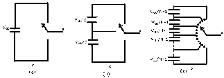
Fig 1(a) shows a two level inverter. Fig 1(b) shows a three level inverter. Fig 1(c) shows N level inverter. All the ca- pacitors comprises to a voltage of Vdc.
Figure 1 Schematic Diagram of (a) Two level Inverter (b) Three Level
Inverter (c) N Level Inverter
Fig 2(a) shows the output voltage of a two level inverter. Fig 2(b) shows the output voltage a three level inverter. Fig 2(c) shows the output voltage of an N level inverter.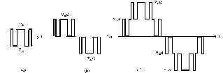
Figure 2 Output Voltage of (a) Two Level Inverter (b) Three Level
Inverter (c) Five Level Inverter
For an N level (between the phase and the negative rail)
diode clamped inverter,
The number of levels in the line-to-line voltage waveform
will be k=2N-1 (1)
The number of levels in the line to load neutral of a star or
wye load will be p=2k-1 (2)
The number of capacitors required, independent of the
number of phase, is Ncap=N-1 (3) While the number of clamping diodes per phase is
Dclamp=2(N-1) (4)
IJSER © 2010 http://www.ijser.org
International Journal of Scientific & Engineering Research, Volume 1, Issue 3, December-2010 2
ISSN 2229-5518
The number of possible switch states is
nstates=Nphases (5)
and the number of switches in each leg is
Sn=2(N-1) (6)
The two basic approaches used to generate the PWM sig- nals for multilevel inverters are
• Sub harmonic or Sub-Oscillation carrier based PWM-modulating waveform comparison with offset triangular carriers
• Space Vector PWM-space vector modulation based on a rotating vector in multilevel space
and these are the extensions of traditional two level con- trol strategies to several levels.
The two main advantages of PWM inverters in compari- son to square-wave inverters are (i) control over output voltage magnitude (ii) reduction in magnitudes of un- wanted harmonic voltages. Good quality output voltage in SPWM requires the modulation index (m) to be less than or equal to 1.0. For m>1 (over-modulation), the fun- damental voltage magnitude increases but at the cost of decreased quality of output waveform. The maximum fundamental voltage that the SPWM inverter can output (without resorting to over-modulation) is only 78.5% of the fundamental voltage output by square-wave inverter. In this paper one more PWM techniques have been consi- dered. The merits and demerits of these two PWM tech- niques are compared under comparable circuit conditions on the basis of factors like (i) quality of output voltage (ii) obtainable magnitude of output voltage (iii) ease of con- trol etc. The peak obtainable output voltage from the giv- en input dc voltage is one important figure of merit for the inverter.
Carrara considered different methods of disposing the many carrier bands required in multilevel PWM.
Four alternative carrier PWM strategies with differing phase relationships for a multilevel inverter [15] are as follows:
1) In-phase disposition (IPD), where all the carriers are in phase- Technique A1;
2) Phase opposition disposition (POD), where the carri- ers above the zero reference are in phase, but shifted by 1800 from those carriers below the zero reference- Technique A2;
3) Alternative phase opposition disposition (APOD), where each carrier band is shifted by 1800 from the ad- jacent bands- Technique A3;
4) Phase Disposition (PD), all the carriers are phase shifted by 2rr/(N-1) radians- Technique B.
In SHPWM technique the intersection of the triangular carrier and the modulation wave determines the genera- tion of the pulse. This requires a carrier of much higher frequency than the modulation frequency. The generated rectilinear output voltage pulses are modulated such that their duration is proportional to the instantaneous value of the sinusoidal waveform at the centre of the pulse; that is, the pulse area is proportional to the corresponding value of the modulating sine wave.
If the carrier frequency is very high, an averaging effect occurs, resulting in a sinusoidal fundamental output with high-frequency harmonics, but minimal low-frequency harmonics.
Steinke [12] proposed SFOPWM, a carrier based method where addition of triplen harmonic to the fundamental frequency Sinusoidal lowers the peak magnitude, thus allowing operating in over modulation region. This in- creases the inverter output voltage without compromis- ing on the quality of the output waveform [3][4].
Equations (9) to (12) are used to obtain the modulating
wave.
Voffset = (max (Va,Vb,Vc ) + min (Va,Vb,Vc ))/2 (9) VaSFO = Va – Voffset (10) VbSFO = Vb – Voffset (11) VcSFO = Vc – Voffset (12)
The zero sequence modification made by the SFOPWM technique restricts its use to three phase three wire sys- tem; however it enables the modulation index to be in- creased by 15.47% before over modulation or pulse drop- ping occurs.
The amplitude modulation index and frequency modula- tion index are given in (13) and (14) respectively.
ma = Am / (m-1)Ac (13) mf = fc / fm (14) Where m is the number of carrier waves also the level of the inverter, required for pulse generation.
A sinusoidal and its modulated wave obtained from
(13), (14) are shown in Fig.3 for a modulation index of 1.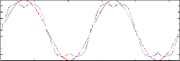
1
0.8
0.6
0.4
0.2
0
-0.2
-0.4
-0.6
-0.8
PD strategy is used most frequently because it pro- duces minimum harmonic distortion for the line–to–line output voltage [13],[14],[15],[16],[17].
-1
0 0.5 1 1.5 2 2.5
Time(s)
Figure 3 Single Phase Modulating Wave
4
x 10
IJSER © 2010 http://www.ijser.org
International Journal of Scientific & Engineering Research, Volume 1, Issue 3, December-2010 3
ISSN 2229-5518
Operation of a multilevel inverter at low switching fre- quency is the Sinusoidal natural PWM and alternately sinusoidal PWM technique is operation at high switching frequency.
A three-phase nine-level diode-clamped inverter is shown in Fig.4 [15][17]. Each phase is constituted by 16 switches (eight switches for upper leg and eight switches for lower leg). Switches Sa1 through Sa8 of upper leg form comple-
low-harmonic distortion waveform characteristics with well-defined harmonic spectrum, the fixed switching fre- quency, and implementation simplicity. Simple tech- niques for generating the modulation waves of the high- performance PWM methods are described. The two novel methodologies Natural Sinusoidal PWM and Sinusoidal PWM for 3rd harmonic injected modulated wave called SFOPWM using constant switching frequency are com- pared[4],[5]. The one most important modulator charac- teristics—the total harmonic distortion is analytically modeled and compared for various carrier pwm methods applied to a nine level Neutral point clamped or Diode clamped inverter. Simulations of the controller and of the inverter have been made in the MATLAB SIMULINK environment.
A nine level inverter is simulated for a normal modula-
’ to S
’ lower leg of the
mentary pair with the switches Sa1 a8
same phase. The complementary switch pairs for phase
tion index of 0.8 and over modulation index of 1.1 at a
switching frequency of 450Hz for Sinusoidal natural
’), (S , S
), (S
, S ’), (S , S
), (S ,
‘A’ are (Sa1, Sa1’), (Sa2, Sa2
a3 a3’
a4 a4
a5 a5’
a6 PWM and 1050Hz for Sinusoidal PWM technique.
’), (S , S
), (S , S
) and similarly for B and C phases
Sa6
a7 a7’
a8 a8’
[1],[2],[3],[4],[5],[6],[7],[8],[17]. Clamping diodes are used
to carry the full load current.
Figure 4 Circuit Diagram of 3 Phase Nine Level Diode Clamped
Inverter
Table 1 shows phase to fictitious midpoint ‘o’ of capacitor string voltage (VAO) and line to line voltage (VAB) for vari- ous switchings’.
TABLE 1
POLE VOLTAGE AND LINE VOLTAGE OF A NINE LEVEL INVERTER
Table 2 show at normal modulation index of 0.8 im- proved performance with reduced harmonic distortion is observed with SPWM technique for A1through B tech- niques for nine level diode clamped inverter.
TABLE 2
LINE-LINE VOLTAGE AND THD FOR NORMAL MODULATION INDEX
SNPWM | SPWM | |||
Vab | THD | Vab | THD | |
A1 | 44.94 | 10.27 | 46.55 | 9.46 |
A2 | 45.53 | 12.24 | 46.72 | 9.29 |
A3 | 45.59 | 11.38 | 46.63 | 9.49 |
B | 59.58 | 17.32 | 60.61 | 13.50 |
A table 3 show at over modulation index of 1.1 im- proved performances with reduced harmonic distortion is observed with SPWM technique for A1through B techniques for nine level diode clamped inverter.
TABLE 3
LINE-LINE VOLTAGE AND THD FOR OVER MODULATION INDEX
SNPWM | SPWM | |||
Vab | THD | Vab | THD | |
A1 | 65 | 7.89 | 65.67 | 6.89 |
A2 | 65.78 | 9.13 | 66.09 | 7.93 |
A3 | 65.84 | 8.55 | 66.02 | 7.42 |
B | 66.49 | 16.51 | 67.1 | 13.39 |
This paper provides analytical methods for the study,
performance evaluation, and design of the modern car-
rier-based PWM’s, like bipolar and unipolar suboscilla- tion carrier PWM methods which are widely employed in PWM multilevel voltage-source inverter drives due to the
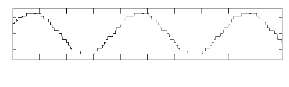
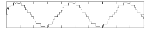
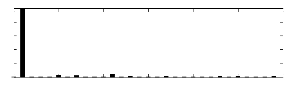
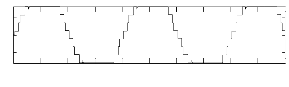
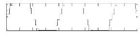
Fig 5 to Fig 10 shows the pole voltage, line voltage and its THD for normal modulation index of 0.8 for phase disposition technique A1 for SNPWM tecchnique with a frequency of 450Hz and SPWM for 1050Hz frequency.
IJSER © 2010 http://www.ijser.org
International Journal of Scientific & Engineering Research, Volume 1, Issue 3, December-2010 4
ISSN 2229-5518
20
0
-20
0 0.005 0.01 0.015 0.02 0.025 0.03 0.035 0.04 0.045 0.05
Time (s)
Figure 5 0.8 A1 SNPW M Pole Voltage
50
0
-50
0 0.005 0.01 0.015 0.02 0.025 0.03 0.035 0.04 0.045 0.05
Time (s)
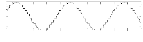
Figure 12 1.1 A1 SNPW M Line Voltage

50
1
0 0.8
Vdc=80V, Fundamental (50Hz) = 65 , THD= 7.89%
-50
0 0.005 0.01 0.015 0.02 0.025 0.03 0.035 0.04 0.045 0.05
Time (s)
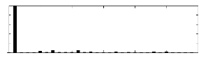
Figure 6 0.8 A1 SNPW M Line Voltage
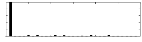
1
0.6
0.4
0.2
0
0 5 10 15 20 25 30
Harmonic order
Figure 13 1.1 A1 SNPW M Line Voltage THD
0.8
Vdc=80V, Fundamental (50Hz) = 44.94 , THD= 10.27%
0.6
0.4 20
0.2
0
20
0 5 10 15 20 25 30
Harmonic or der
Figure 7 0.8 A1 SNPW M Line Voltage THD
0
-20
0 0.005 0.01 0.015 0.02 0.025 0.03 0.035 0.04 0.045 0.05
Time (s)
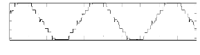
Figure 14 1.1 A1 SPW M Pole Voltage
10
0
-10 50
-20
40
20
0
0 0.005 0.01 0.015 0.02 0.025 0.03 0.035 0.04 0.045 0.05
Time (s)
Figure 8 0.8 A1 SPW M Pole Voltage
0
-50
0 0.005 0.01 0.015 0.02 0.025 0.03 0.035 0.04 0.045 0.05
Time (s)

Figure 15 1.1 A1 SPW M A1 Line Voltage
-20
-40
0 0.005 0.01 0.015 0.02 0.025 0.03 0.035 0.04 0.045 0.05
Time (s)
Figure 9 0.8 A1 SPW M Line Voltage
1
0.8
0.6
0.4
Vdc=80V, Fundamental (50Hz) = 65.67 , THD= 6.89%
0.2
1
0.8
0.6
Vdc=80V, Fundamental (50Hz) = 46.65 , THD= 9.46%
0
0 5 10 15 20 25 30
Harmonic order
Figure 16 1.1 A1 SPW M Line Voltage THD
0.4
0.2
0
0 5 10 15 20 25 30
Harmonic order
Figure 10 0.8 A1 SPW M Line Voltage THD
A third harmonic injected modulated wave is used to generate the gating signals for a modeled nine level diode
Fig 10 to Fig 16 shows the pole voltage, line voltage and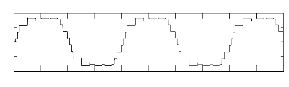
its THD for over modulation index of 1.1 for phase disposition technique A1 for SNPWM tecchnique with a frequency of 450Hz and SPWM for 1050Hz frequency.
40
20
0
-20
-40
0 0.005 0.01 0.015 0.02 0.025 Time (s) 0.03 0.035 0.04 0.045 0.05
Figure 11 1.1 A1 SNPW M Pole Voltage
clamped multilevel inverter. The technique SPWM has shown improved performance over SNPWM technique.
[1] José Rodríguez, Jih-Sheng Lai, Fang Zheng Peng “Multilevel Inverters: A Survey of Topologies, Controls, and Applications”, IEEE Trans., VOL. 49, NO. 4, AUGUST 2002
[2] G.Carrara, S.Gardella, M.Marchesoni, R.Salutari and G.Sciutto,
“ A New Multilevel PWM Method: A theoretical Analysis”,
IEEE Transactions on Power Electronics, Vol. 7, No. 3, July
1992, pp.497-505.
[3] A. Nabae, I. Takahashi, H. Akagi. “A neutral-point clamped
PWM inverter”, IEEE Trans. on I.A., Vol. IA-17, No. 5, 1981, pp.
518-523.
[4] P.Palanivel1, Subhransu Sekhar Dash, “Comparative Study of Constant Switching Frequency and Variable Switching Frequency Multicarrier Pulse width Modulation for Three Phase Cascaded Mul-
IJSER © 2010 http://www.ijser.org
International Journal of Scientific & Engineering Research, Volume 1, Issue 3, December-2010 5
ISSN 2229-5518
tilevel Inverter”., International Journal of Recent Trends in Engi- neering, Vol 2, No. 7, November 2009.
[5] P.Palanivel1, Subhransu Sekhar Dash, “Multicarrier Pulse Width Modulation Based Three Phase Cascaded Mulitilevel Inverter Includ- ing Over Modulation and Low Modulation Indices”, International Journal of Engineering Studies ISSN 0975- 6469 Volume 1, Number 2 (2009), pp. 71–82
[6] A. Nabae, I. Takahashi, and H. Akagi, “A new neutral-point- clamped PWM inverter,” IEEE Trans. Ind. Applicat., pp. 518–
523, Sept./Oct.1981.
[7] J. S. Lai and F. Z. Peng, “Multilevel converters—A new breed of power converters,” IEEE Trans. Ind. Applicat., Vol. 32, pp. 509–
517, May/June 1996.
[8] M. Carpita, M. Fracchia. S. Tenconi. “A novel multilevel struc-
ture for voltage source inverter”, Proceedings of the 4th Euro-
pean Conf, on Power Electronics and Applications (EPE’91), Firenze, Italy, September 1991, pp.1-090/1-094.
[9] J. Holtz, “Pulsewidth modulation—A survey,” IEEE Trans. Ind.
Electron., Vol. 39, pp. 410–420, Oct. 1992.
[10] Nguyen Van Nho, Quach Thanh Hai, Hong Hee Lee,” Carrier
Based Single-State Pwm Technique In Multilevel Inverter”, Inter- national Symposium on Electrical & Electronics Engineering
2007 - Oct 24, 25 2007
[11] B. P. McGrath, D.G. Holmes, M. Manjrekar, T. A. Lipo, “An
Improved Modulation Strategy For A Hybrid Multilevel Inver- ter”2000.
[12] J.K. Steinke, “Control Strategy for a Three Phase AC Traction
Drive with a 3-level GTO PWM Inverter”, IEEE PESC, 1988, pp.
431-438.
[13] Ivo Pereira, António Martins, “Experimental Comparison of Car-
rier and Space Vector PWM Control Methods for Three-Phase NPC
Converters” International Conference on Renewable Energies and Power Quality (ICREPQ’09), Valencia (Spain), 15th to 17th April, 2009.
[14] A.Tahri, A.Draou “A Comparative Modelling Study of PWM Control Techniques for Multilevel Cascaded Inverterr”, Leo- nard Journal of Sciences ,Jan-Jun 2005 , pp 42-58.
[15] leon M. Tolbert, Fang Z.Peng, ,Thomas G. Habetler, “Multile- vel PWM Methods at Low Modulation Indices” APEC ’99, Dallas, Texas, March 14-18, pp 1032-1039.
[16] Leon M. Tolbert, Fang Z.Peng, ,Thomas G. Habetler, “Novel Multilevel Inverter Carrier-Based PWM” IEEE IAS 1998, Mis- souri, October 10-15, 1998, pp. 1424-1431.
[17] Samir Kouro, IEEE, Pablo Lezana, Mauricio Angulo, and José Rodríguez, “MulticarrierPWMWith DC-Link Ripple Feedforward compensation for Multilevel Inverters” IEEE Transactions On Power Electronics, VOL. 23, NO. 1, JANUARY 2008.
[18] Jang-Hwan Kim, Seung-Ki Sul and Prasad N. Enjeti, “A Carri- er-Based PWM Method with Optimal Switching Sequence for a Multi-level Four-leg VSI” IEEE , June 2005, pp 99-105. for
spwm,sfopwm ,npc.
IJSER © 2010 http://www.ijser.org