Outputs: Sum(S), Carry (C).
International Journal of Scientific & Engineering Research, Volume 6, Issue 1, January-2015 579
ISSN 2229-5518
Modular versus Monolithic Digital Circuit Design: Effect on Propagation Delay and Glitch
Adeniran Adetunji, Akande Ademola, Babalola M. Florence.
Abstract— This paper reviews the concept of modular design method with respect to digital circuit design. It discusses the propagation delay and glitches as expected in a real digital circuit design, using full adder circuit as an experimental example, an analysis of a monolithic versus modular design methods of full adder circuit shows a better performance when digital circuits/systems are designed in modules.
Index Terms – Digital Circuit, Verilog HDL, Modular design, Monolithic design, Glitch, Propagation Delay, Logic gates.
—————————— ——————————
consequences; overall finite delay in circuit response
I. INTRODUCTION
Modularity is an established technique for organizing and simplifying a complex digital system, it is a process where we build up devices e.g. Digital systems from a set of distinct components like basic logic gates or modules (combinations of two or more logic gates). It is an established fact that Modular system is advantageous in terms of its scalability, flexibility, simplicity, portability, even the debated reliability of modular system that “more parts equals greater risk of failure”, as been proven to be incomplete and at worst misleading.
Modularity in system design has an inherent fault
tolerance and provides powerful new defence against system failure, [2].
The time associated with any digital circuit for an input change in the circuit to propagate through the circuit and changes the output is known as its propagation delay. Any digital system not matter how complex can be broken down into its cell units called digital gates (And, OR, Not, …). Each of these gates has its own propagation delay and for the single gate this delay can be very short and insignificant but when considering larger circuit of which they are components, the delay may be significant and call for consideration in design.
When analysing digital circuit ideally, we may assume a
stable circuit; input have been applied a long time ago and they have never changed since, so that all gates have had enough time to compute their outputs or that all the gate components of the circuit are ideally fast- they react immediately to the changes at the input. In contrast, real digital circuit has transient behaviour as explained earlier, each gate has a finite (not 0) delay from the time inputs change to the time the change effects their outputs. This transient behaviour of digital circuit has two main
which is a major determinant of digital circuit performance evaluation and Glitches at their outputs. A glitch is an invalid and unpredicted output of a digital circuit usually caused by propagation delay.
In this paper, we want to compare the effect of two contrast design methods; monolithic design and Modular design on Performance (circuit delay) and Glitch (invalid output) in Full Adder Circuits. Our methodology is to start from analysis of half adder circuit, design the logic gate, model and simulate it in verilog.
An analysis of full adder circuit and its design modelled
in two ways; first using the basic gate components in a monolithic design, and by using two modules of half adder with an OR gate in a modular design method. An equal time delay is assumed for each basic gate in the design. Simulating the two designs, an observation of any discrepancy in performance and glitches at the output and compared.
II. HALF ADDER CIRCUIT ANALYSIS
A. Table 1 Half Adder Truth Table
A | B | S | C |
0 | 0 | 0 | 0 |
0 | 1 | 1 | 0 |
1 | 0 | 1 | 0 |
1 | 1 | 0 | 1 |
B. Boolean expression for Half Adder Circuit
Input: A, B
Outputs: Sum(S), Carry (C).![]()
![]()
S = AB + AB = A ⊕ B
C = AB
IJSER © 2015 http://www.ijser.org
International Journal of Scientific & Engineering Research, Volume 6, Issue 1, January-2015 580
ISSN 2229-5518
Figure 1.2: Half Adder model and simulation.
C. Figure 1.1 Logic Circuit Diagram for Half Adder
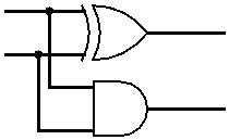
A
S B
C
D. Verilog Code for Half Adder
//--------------------------------//Verilog model of Module_1 (Half adder) with Verilog HDL
module H_Adder (S, C, A, B);
input A, B; output C, S; xor (S, A, B); and (C, A, B); endmodule
//--------------------------------
//--------------------------------
// Test bench for H_Adder module t_H_Adder;
reg A, B;
wire S, C;
H_Adder H_A1 (S, C, A, B); // Instance name required initial
begin
A = 1'b0; B = 1'b0;
#100 A = 1'b0; B = 1'b0;
#100 A = 1'b0; B = 1'b1;
#100 A = 1'b1; B = 1'b0;
#100 A = 1'b1; B = 1'b1;
end
initial #500 $finish;
endmodule
//--------------------------------
The code and analysis of half adder above assume and
ideal logic gates. Let’s assume a basic gate delay of 10ns for each logic gates as in verilog code bellow.
//--------------------------------
//Verilog model of Module_1 (Half adder) with
//Verilog HDL
module H_Adder (S, C, A, B);
input A, B;
output C, S;
xor #(10)(S, A, B); and #(10)(C, A, B); endmodule
//--------------------------------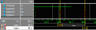
Figure 1.3: Half Adder model and simulation with assumed gate delay.
It can be observed that from the simulation that the circuit output was delayed for 10ns after the change in input at 200ns and 400ns.
III. FULL ADDER ANALYSIS
A. Table 2.1 Full Adder Truth Table
A | B | Cin | S | Cout |
0 | 0 | 0 | 0 | 0 |
0 | 0 | 1 | 1 | 0 |
0 | 1 | 0 | 1 | 0 |
0 | 1 | 1 | 0 | 0 |
1 | 0 | 0 | 1 | 0 |
1 | 0 | 1 | 0 | 1 |
1 | 1 | 0 | 0 | 1 |
1 | 1 | 1 | 1 | 1 |
IJSER © 2015 http://www.ijser.org
International Journal of Scientific & Engineering Research, Volume 6, Issue 1, January-2015 581
ISSN 2229-5518
B. Boolean Analysis of full adder
![]()
![]()
![]()
![]()
S = ABCin + ABC in + ABC + ABCin
![]()
![]()
![]()
![]()
= ABCin + ABCin + ABC in + ABC in
![]()
![]()
![]()
![]()
= Cin ( AB + AB) + C in ( AB + AB)
![]()
![]()
= Cin ( A ⊕ B) + C in ( A ⊕ B)
Let A ⊕ B = P , then;
![]()
![]()
S = Cin P + C in P
![]()
![]()
= Cin ⊕ P.
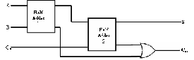
Figure 3.3: Full adder circuit two modules of half adder
E. Verilog Code for full adder circuit in Figure 2.3
//--------------------------------
//Verilog model of Module_1 (Half adder) with
Cout
![]()
![]()
![]()
![]()
= ABCin + ABCin + ABC in + ABCin
// Verilog HDL
module Full_Adder_1 (S, Cout, A, B, Cin);
= Cin ( AB + AB) + AB(C in + Cin )
= Cin ( A ⊕ B) + AB
= Cin P + AB
C. Figure 2.1: Logic circuit of full adder in a monolithic design.
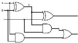
S Cout
Figure 2.1: Monolithic design of Full Adder logic circuit
D. Figure 2.2: Logic circuit of full adder designed using two modules o f half adder.
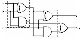
Figure 2.2: Modular design of Full adder logic circuit
In figure 2.2, the broken lines represents an Half adder and the complete full adder circuit composed of two half adder module and an OR gate, is in block diagram of figure 2.3.
input A, B,Cin; output S, Cout; wire w1, w2, w3;
xor E1(w1, A, B);
xor #(10)E2(S, w1, Cin);
and #(10)A1(w2, w1, Cin);
and #(10)A2(w3, A, B);
or #(10)O1(Cout, w2, w3);
endmodule
//--------------------------------
//--------------------------------
// Test bench for Full_Adder_1 module t_Full_Adder_1;
reg A, B, Cin;
wire S;
wire Cout;
Full_Adder_1 FA1(S,Cout, A, B, Cin);
initial begin
A= 1'b0; B = 1'b0; Cin = 1'b0;
#100 A= 1'b0; B = 1'b0; Cin = 1'b1;
#100 A= 1'b0; B = 1'b1; Cin = 1'b0;
#100 A= 1'b0; B = 1'b1; Cin = 1'b1;
#100 A= 1'b1; B = 1'b0; Cin = 1'b0;
#100 A= 1'b1; B = 1'b0; Cin = 1'b1;
#100 A= 1'b1; B = 1'b1; Cin = 1'b0;
#100 A= 1'b1; B = 1'b1; Cin = 1'b1;
end
initial #800 $finish;
endmodule
//--------------------------------
IJSER © 2015 http://www.ijser.org
endmodule
//--------------------------------
582
(a)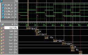
(b)
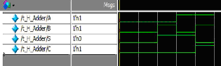
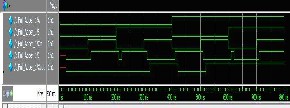
We can observe as analysed in figure 3.4(b);
i. 10ns delay in output after input change at 100ns,
ii. A10ns glitch (between 210-220ns) after input change at
200ns
iii. An overall delay of 20ns after input change at 300ns iv. An overall delay of 20ns after input change at 400ns v. Overall delay of 20ns after input change at 500ns
vi. A 10ns glitch (between 610-620) after input change at
600ns
vii. 10ns delay of output after input change at 700ns
Average circuit delay can be given by;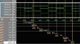
(a)
We can observe as analysed in figure 3.5(b);
i. 10ns delay in output after input change at 100ns,
ii. 10ns glitch (between 210-220ns) after input change at
200ns
iii. An overall delay of 10ns after input change at 300ns
iv. An overall delay of 10ns after input change at 400ns v. Overall delay of 10ns after input change at 500ns
vi. A 10ns glitch (between 610-620) after input change at 600ns
vii. 10ns delay of output after input change at 700ns
Average circuit delay for modular full adder circuit design
TDAV
=
total
![]()
Total number
delay of
time input
change
as in figure 3.3 can thus be given by;![]()
= 100 = 20ns
5
TDAV =
70
total
Total
![]()
number
delay
of
time
input
change
E. Verilog Code for full adder circuit.
//--------------------------------//Verilog model of Module_1 (Half adder) with Verilog HDL![]()
= = 14ns
5
III. CONCLUSION
module full_Adder_2 (S, Cout, A, B, Cin);
input A, B,Cin; output S, Cout; wire w1, w2, w3;
H_Adder HA1 (w1, w2, A, B); H_Adder HA2 (S, w3, w1, Cin);
or (Cout, w3, w2);
If can be inferred from the circuit analysis and simulation above that, the overall performance and reliability of the circuit is improved using modular design methodology rather that monolithic design with the basic logic gates.
The performance is indirectly proportional to the overall delay of the digital circuit/system. Thus it can be said that a circuit or system designed in modules is approximately more 30% efficient in terms of speed than a system designed monolithically. Though the glitches produced
IJSER © 2015 http://www.ijser.org
583
were the same for the two scenarios but, the overall delay
time was reduced in when the full adder circuit is designed in modules of half adder.
Other methods can be recommended for removal of glitch; all the same, we’ve been able to establish that digital design in modules enhances circuit performance and reliability.
IV. REFERENCES
Introduction to the Verilog HDL, Fifth Edition. Copyright © 2013, 2007,
2002, 1991, 1984 Pearson Education, Inc.
Evolution of Reliability” White Paper 76, Revision 1, Schneider Electric.
IJSER © 2015 http://www.ijser.org