International Journal of Scientific & Engineering Research Volume 2, Issue 4, April-2011 1
ISSN 2229-5518
Mn DOPED SnO2 Semiconducting Magnetic
Thin Films Prepared by Spray Pyrolysis Method
K.Vadivel, V.Arivazhagan, S.Rajesh
Abstract -- Semiconducting magnetic thin films of SnO2 doped with Mn was prepared by spray pyrolysis method. The polycrystalline nature of the films with tetragonal structure was observed from X-ray Diffractometer. The calculated cryst alline size was 16-22 nm and the lattice constant is a=4.73Ao and c=3.17Ao. The compositional studies give the weight percentage of the used materials. The absorption edge starts with 294 nm and rise in transmittance spectra shows the nanocrystalline effect of as deposited films. The calculat ed band gap from the absorption coefficient is 3.25 eV which great er than the bulk band gap of Tin oxide. The electrical properties of the prepared films also reported in this paper.
Index Terms -- Mn doped SnO2, Spray Pyrolysis, XRD, UV, Electrical study.
—————————— • ——————————
1. INTRODUCTION
HE study of SnO2 transparent conducting oxide thin films are of great interest due to its unique attractive properties like high optical transmittance, uniformity, nontoxicity, good electrical, low resistivity, chemical inertness, stability to heat treatment, mechanical hardness, Piezoelectric behavior and its low cost. SnO2 thin films have vast applications as window layers, heat reflectors in solar cells, flat panel display, electro-chromic devices, LEDS, liquid crystal displays, invisible security circuits, various gas sensors etc. Undoped and Cu, Fe and Mn doped SnO2 thin films have been prepared by vapor deposition technique and reported that SnO2 belongs to n-type semiconductor with a direct optical band gap of about 4.08 eV [6]. To improve the quality of the films as well as the
physical and chemical properties, the addition of some metal ions as
impurities is expected to play an important role in changing the charge carriers concentration of the metal oxide matrix, catalytic activity, the surface potential, the phase composition, the size of crystallites, and so on [8- 10]. It is expected that various concentration of Mn in SnO2 may affect the structural, optical and magnetic properties of the films. From bang gap engineering point of view, suitable band gap is essential for the fabrication of optical devices. So far our knowledge is concerned there are very few reports available on the deposition of Mn doped SnO2 thin films by spray pyrolysis method. In considering the importance of these
materials in the field of magnetic materials, we have prepared Mn doped SnO2 films using a simple and locally fabricated spray pyrolysis system relatively at the temperature of 450°C.
2. EXPERIMANTAL
Mn doped SnO2 thin films were prepared by spray pyrolysis method. Mn doped SnO2 thin films were prepared by spray pyrolysis method. The starting materials were SnCl4.5H2O for Tin and Mn(CHOO3)2.4H2O for Manganese.The concentration of 0.5m of Stannous chloride and 0.1m of Manganese acetate was taken in two different beakers with double distilled water. Then 98% of Stannous chloride solution and 2% of manganese acetate solution was mixed together and stirred using
magnetic stirrer for 4 hours and allowed to aging for ten days. The clear solution of the mixer was taken for film preparation by spray
pyrolysis method. The temperature of the substrate in this method
for preparing nanocrystalline films plays an important role. Here the temperature of the substrate kept at 450aC and the solution was sprayed using atmospheric air as carrier gas. Then the film was allowed to natural cool down. The structural studies on as deposited manganese doped tin oxide thin films were analyzed using X-Ray
diffractometer (Shimadzu XRD-6000). Using EDAX (JSM
6390) the elemental composition of the films was carried out. The optical and electrical properties of the films done by UV-Vis spectrometer (Jasco-570 UV/VIS/ NIR) and Hall (Ecopia HMS-
3000) measurement system.
IJSER © 2011 http://www.ijser.org
International Journal of Scientific & Engineering Research Volume 2, Issue 4, April-2011 2
ISSN 2229-5518
3. RESULT AND DISCISSION
3.1. Structural studies on Mn:SnO2 thin films
The structural studies on as deposited Mn doped Tin oxide were analyzed by X-Ray spectrophotometer and the graph between 2 theta versus diffracted ray intensity is shown in figure 1.
The polycrystalline natures of the prepared samples were observed
from large number of diffracted peaks. The tetragonal structure of the sample with the three strong peaks of (1 1 0), (1 0 1) and (2 1 1) correspond with peak position of 28=26.3609, 33.6541 and 51.6145
respectively were identified using standard JCPDS files.
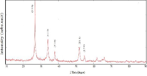
Fig 1. XRD pattern of Mn doped SnO2 nanocrytalline thin films
Substrate temperature is one of the main parameters, which
determine the structural properties of the films. The crystalline size
of as deposited films were calculated using Debye-Scherrer’s
formula given by,


--------------------- (1)
Where 'A is the wavelength of X-ray used (1.54 Aa), � is the full width half maximum (FWHM) of the peak and 8 is the glancing
,
angle. The lattice constant of the spray coated Tin oxide films calculated using the formula

-------------------- (2)
Where‘d’ is the interplanar distance, (h k l) are the Miller indices
and ‘a’ and ‘c’ are the lattice constant for the Tetragonal structure.
The calculated crystalline size (D) and lattice constant (a and c) of
spray coated Mn doped Tin oxide are tabulated in table 1.
Table.1. Structural parameters of Mn doped SnO2


Substrate temperature
h k l d
(Aa)
28 FWHM (�)
D (Aa)
c
(Aa )
a
(Aa)
450a C
1 1 0
1 0 1
2 1 1
3.3420
2.6342
1.7608
26.6517
34.0089
51.8835
0.3699
0.4690
0.5271
220
177
167
3.17 4.73

IJSER © 2011 http://www.ijser.org
International Journal of Scientific & Engineering Research Volume 2, Issue 4, April-2011 3
ISSN 2229-5518
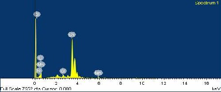
Fig 2. The EDAX spectrum of as deposited Mn doped Tin Oxide thin films
Fig 2 shows,The EDAX spectrum shows the compositional wt % of the used materials. The weight and atomic percentage of Sn was
observed as 122.96 % and 23.65 % respectively. The weight and
atomic percentage of doped Mn was observed as 1.09 % and 0.45 %
respectively.
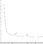
3.3. Optical studies on SnO2 thin film
The optical studies of the Mn doped films were studies by
UV –Vis spectrometer in the range of 200-900 nm. The absorption edge starts with 294 nm reveals that the Nanocrystalline effect of
the films. Also the absorption peaks around 400 nm and 550 nm
(indicated by arrow) observed in the graph shown in fig 3.
1.6
1.4
1.2
1.0
0.8
0.6
0.4
0.2
300 400 500 600 700 800
Wavelength(nm)
45
40
35
30
25
20
15
10
5
0
300 400 500 600 700 800 900
Wavelength (nm)
Fig 3. Absorption and transmittance spectra of Mn doped Tin oxide thin films
The light transmitted spectra have the maximum transmittance of 40 percentage is shown in fig 3. The rise in transmittance spectra
observed at around 500 nm and 700 nm may be due to
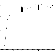
nanocrystalline effect of as deposited films. The optical band gap of the film was calculated using absorption coefficient. The band gap value could be obtained from the optical absorption spectra by using Tauc’s relation [12],

--------------------------- (3)
Where a is the absorption coefficient, ( ) is the photon energy and A is a constant. The direct band gap semiconductor
can be obtained from the relation,
IJSER © 2011 http://www.ijser.org
International Journal of Scientific & Engineering Research Volume 2, Issue 4, April-2011 4
ISSN 2229-5518

100
90
80
70
60
50
40
30
20
10
(4)
0
0.0 0.5 1.0 1.5 2.0 2.5 3.0 3.5 4.0
Photon energy (eV)
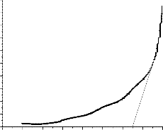
Fig 4. Optical band gap plot between photon energy versus absorption coefficient

Fig.4 shows the variation of ( 2 versus ( ) for the SnO2 thin film. The straight nature of the films over the wide range of photon energy indicates the direct type of transition. The optical gap has then been determined by extrapolation of the linear region on the energy axis shown in fig.4. The optical band gap of 3.25 eV was
3.3. Electrical properties of Mn doped SnO2 films
The electrical properties of the prepared films carried out using Hall measurement system at room temperature with the given input voltage of 1 mA. The negative sign of the Hall coefficient value of -3.666x10⁻³ shows the n-type semiconducting nature of the
films. The conductivity (cr) and resistivity (cr) of the film observed
observed in films prepared at 450aC of substrate temperature. It clearly shows the observed value of band gap is greater than the bulk band gap (2.5 eV) of Tin oxide.
as 2.161x10³ 0.-1cm-1 and 4.628 x10⁻⁴ O.cm respectively. The carrier concentration of the Mn doped SnO2 have the value of minus 1.703x1021cm-2. The mobility of the films were found as
7.922 cm2/V.sec . From these result is observed that the Mn doped
SnO2 films have good electrical properties.
4. CONCLUSION
Manganese doped Tin oxide thin films were prepared by spray pyrolysis method. The X-ray diffractogram shows the polycrystalline nature of as deposited films with tetragonal structure. The crystalline size of the film was calculated using Debye-Scherer formula is varies from 16-22 nm corresponds to three strong peaks. The calculated lattice constant of the films from
interplanar distance and peak plane is a=4.73Aa and c=3.17Aa.
The optical studies reveals that the presence of nanoparticle on the films. The signature of nanocrystalline effect of as deposited film is absorption edge (294 nm) and the rise in transmittance spectra. The calculated band gap of 3.25 is greater than the bulk band of value of Tin oxide. The n-type semiconducting nature of the films observed from negative sign of the Hall coefficient. The conductivity of
2.161x10³ 0.-1cm-1 was observed on as deposited films.
REFERNCES
[1].Arivazhagan.V , Rajesh.S, Journal of Ovonic research, Vol.6,No.5 ,221-226 ,(2010)
[2] J. B. Yoo, A. L. Fahrenbruch, R. H. Bube, J Appl Phys. 68, 4694
(1990).
[3] R. S. Rusu, G. I. Russia, J. Optoelectron. Adv. Mater 7(2), 823 (2005).
[4] M. Penza, S. Cozzi, M. A. Tagliente, A. Quirini, Thin Solid
Films, 71, 349 (1999).
IJSER © 2011 http://www.ijser.org
International Journal of Scientific & Engineering Research Volume 2, Issue 4, April-2011 5
ISSN 2229-5518
[5] S. Ishibashi, Y. Higuchi, K. Nakamura, J. Vac. Sci. Technol.,
A8, 1403 (1998).
[6] J. Joseph, V, K. E. Abraham, Chinese Journal of Physics, 45,
No.1, 84 (2007).
[7] E. Elangovan, K. Ramamurthi, Cryst. Res. Technol., 38(9), 779 (2003).
[8]. Datazoglov O. Thin Solid Films, Vol.302, 204-213,(1997)
[9]. Fantini M. and Torriani I. Thin Solid Films, Vol.138, 255-265
,(1986).
[10]. Garcia F.J., Muci J. and Tomar M.S. Thin Solid Films, Vol.97,
47-51,(1982)
[11]. Z. C. Jin, J. Hamberg, C. G. Granqvist, J Appl Phys.64, 5117 (1988).
[12].Advani G.N et al, Thin Solid Films, 361 367,(1974)
[13]. Badawy W.A et al Electrochem, Soc., Vol.137, 1592-
1595,(1990)
[14]. Bruneaux J et al,Thin Solid Films, Vol.197, 129-142,(1991) [15]. Chitra Agashe et al. J. Appl. Phys. Vol.70, 7382-7386,(1991) [16]. Chitra Agashe et al, Solar Energy Mat.,Vol.17 ,99-117,(1988) [17]. Datazoglov O. Thin Solid Films, Vol.302, 204-213,(1997)
[18]. Fantini M. and Torriani I. Thin Solid Films, Vol.138, 255-265
,(1986).
[19]. Garcia F.J., Muci J. and Tomar M.S. Thin Solid Films, Vol.97,
47-51,(1982)
[20]. Ghoshtagore R.N. J. Electrochem. Soc., Vol.125, 110-
17,(1978)
[21]. Segal and Woodhead J L Proc.Br.Ceram.Soc.38, 245, 1986

*Corresponding Author
K.Vadivel*, V.Arivazhagan, S.Rajesh- Research Department of
Physics, Karunya University, Coimbatore, Tamilnadu, India-641
114. *Email: vadivelphyphd08@gmail.com
IJSER © 2011 http://www.ijser.org