The research paper published by IJSER journal is about Mixed signal IC (CP-PLL) Testing scheme using a novel approach 1
ISSN 2229-5518
Mixed signal IC (CP-PLL) Testing scheme using a novel approach
Ashish Tiwari, Anil Kumar Sahu
Abstract— An effective novel approach for built in self test is proposed in this paper, which is useful in Mixed signal IC testing (here CP- PLL). The approach is useful in digital testing applications which can detect the fault in any of the block that is phase frequency detector, VCO, loop filter, or charge pump. The key advantage of this approach is that it uses all the existing elements for measuring and testing which reduces the area overhead for testing scheme. Restated, that the proposed architecture does not alter the analog blocks. Rather the proposed approach adds small circuits to PLL with slight modification for digital part. The testoutput generated is purely a digital output which certainly increases the realiability of the proposed BIST structure. A fault simulation result shows the charactericsti cs of the BIST structure that is high fault coverage of 98%. The implemtation is done using the Tanner, VHDL and waveforms are made using the T- Spice.
Index Terms— Area overhead, BIST, CP-PLL, IC, fault coverage, Phase frequency detector, testing, VCO.
—————————— ——————————
HIS paper proposes a novel approach for Mixed signal ICs here CP-PLL. The approach adopted consists of Built in Self Test Architecture which incorporates the exixting
elements of CP-PLL. Phase-locked loops (PLLs) have been used extensively in phase compensation across the clock tree and in synchronizing the operation of different cores on the system on chip. Additionally, a PLL may serve as a clock mul- tiplier or divider on nonbinary ratios that can be easily changed on the fly for saving power and reducing the impact of noise on other circuits. The growing popularity of PLLs has increased the need for testing these devices during prototyp- ing and production. The PLL is one of the most commonly used mixed-signal building blocks in IC design. In some ap- plications, designers may not consider the PLL a ―mixed- signal‖ function because it has digital inputs and digital out- puts. Testing PLLs on a synchronous digital tester or a mixed- signal tester thus can involve complex programming [1]. Ac- cordingly, PLLs frequently are tested by simply checking that they achieve the phase lock. Such tests may be insufficient to ensure adequate lock range and loop stability under all condi- tions. The traditional procedure for testing an analog device is to provide an input signal and measure the output response. For example, to obtain the frequency response of a filter, a sine-wave is used to stimulate the circuit, and the amplitude and phase of the output signal then are evaluated. However, testing an arbitrary analog device may be very expensive. The signal sources and measuring instrumtents can be complex, especially for PLLs [2].
The obvious key to the success of products with these properties is the built-in self-test (BIST) of circuits and sys-
tems.
————————————————
![]() Ashish Tiwari is currently pursuing master’s degree program in electronics and telecommunication engineering specialization in VLSI Design in SSCET, Bhiali, India, and PH-09755863513.
Ashish Tiwari is currently pursuing master’s degree program in electronics and telecommunication engineering specialization in VLSI Design in SSCET, Bhiali, India, and PH-09755863513.
E-mail: tiwari.ashish99@gmail.com
![]() Anil Kumar Sahu is currtest 1ly working as Assistant Professor in electronics and telecommunication engineering departmtest 1 in SSCET, Bhilai ,
Anil Kumar Sahu is currtest 1ly working as Assistant Professor in electronics and telecommunication engineering departmtest 1 in SSCET, Bhilai ,
India, PH-9926811371, E-mail:anilsahu82@gmail.com
The inclusion of BIST capabilities at the chip level reduces the
need for high-performance test equipments. Although BIST is widely used for digital integrated circuit IC‘s, manufacturers of mixed Signal ICs are still seeking suitable techniques for applying BIST to analog circuits [3]–[5]. A key for IC manufac- turers is the ―overhead‖ required to implement BIST on their systems. This paper proposes a new BIST structure using the existing charge pump as the stimulus generator and the vol- tage-controlled oscillator (VCO) as the measuring devices to reduce area overhead. The proposed BIST structure has mi- nimal area overhead and does not need to load any analog nodes of the PLL. The remainder of this paper is organized as follows. Section 2 reviews some previousworks on PLL tes ing. Section 3 then describes the circuit under test; section 4 is about proposed BIST structure of the PLL and elucidates the testing procedure. Some test considerations are discussed in Section 5. Subsequently, simulation results are presented in Section 6. Section 7 draws conclusions.
The rectest 1 literature of PLL testing is covered in [2]–[9]. Refe ences [2] and [3] describe the on-chip measuremtest 1 of the jitter transfer function and emphasize on-chip jitter generation and output jitter measuremtest 1. While this technique has solved the test accessibility problem by building a signal gene- rator and a signature analyzer for the PLL, it suffers from high die area overhead and analog node loading problems. The analog nodes can easily be loaded to alter the loop characteris- tics. PLL systems convtest 1ionally have been tested based on functional specifications, and circuit functionality is verified at some prespecified test points. This method can lead to either excessive or insufficitest 1 circuit testing [4], [5]. Fault-based
IJSER © 2012
The research paper published by IJSER journal is about Mixed signal IC (CP-PLL) Testing scheme using a novel approach 2
ISSN 2229-5518
testing is an attractive alternative to functional testing which targets the presence of physical defects in a PLL, including parametric and structural faults, thus providing a quantitative measure of the test process [6]. BIST schemes which involve defect-oritest 1ed testing can eliminate die area overhead and analog node loading problem, but only test some blocks of the PLL, rather than the test 1ire PLL [7]–[9]. Fault coverage thus is low due to some faults in the PLL’s being impossible to detect. Possible faults in any block of the PLL can be detected using the proposed BIST structure. The proposed scheme uses an existing charge-pump as the stimulus generator, removing the need for any test stimulus. Additionally, the VCO is adopted as measuring devices during testing. The main ad- vantage of this approach is that the analog blocks of PLL are unchanged and the test output is purely digital, ensuring that the characteristics of PLL are unaltered and a Suitable on-chip design can be designed using the proposed BIST structure.
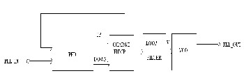
Fig. 1. Block diagram of classical CP-PLL
A PLL is a feedback control loop circuit that synchronizes an output signal (generated by an oscillator) with a reference or input signal in both frequency and phase. Fig. 1 shows the block diagram of the classical CP-PLL [6], [7], which consists of the following four functional blocks:
1) phase/frequency detector (PFD);
2) charge-pump circuit, which transforms the digital Up and
Down signals into analog voltages;
3) Loop filter, which attenuates the high-frequency compo-
nents from the analog voltage generated by the chargepump
circuit;
4) VCO, which generates a clock, with the frequency of the clock being controlled by control voltage Ctrl_V generated by the loop filter.
The PFD compares the output signal PLLClk_out generated by the VCO with reference-input signal PLLClk_in. A classical
three-state PFD is considered to be built with four flip-flops and some gating logic. It generates two output signals, i.e., Up and Down, which depend on the phase difference and the fre- quency difference. The state diagram of the PFD is shown in Fig. 2. At the falling edge of signal PLLClk_in, i.e., PLLClk_in
↓, one of three changes can occur:
1) Transition from states 1 to 0, i.e., resetting Down;
2) Transition from states 0 to 2, i.e., setting Up;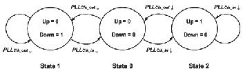
Fig. 2. State diagram of the PFD
3) No change, output remains in state 2.
At the falling edge of signal PLLClk_out, i.e., PLLClk_out ↓,
transitions take place in a similar way. Notably, signals Up
and Down are used to increase and decrease the frequency of
signal PLLClk_out, respectively. Then, the combination of the
charge-pump circuit and the loop filter converts these digital signals into an analog control voltage for the VCO. Basically, the charge-pump circuit consists of two CMOS switches con- trolled by the PFD output. It converts the PFD‘s logic states into a ternary signal that can be one of three valid states: 1) logic 1 when the Up signal is high; 2) logic 0 when the Down signal is high; and 3) a highimpedance state when neither sig- nal is high. In the third case, the output voltage depends only on the loop-filter components. Fig. 3 shows the RTL schematic of the PFD based upon the state diagram. A simple second- order, low-pass filter composed of a resistor and two capaci- tors is considered to filter this ternary signal.
Finally, the VCO delivers output signal PLLClk_out, whose
frequency is proportional to the analog control voltage applied
at its input. This paper considers a classical VCO based on a
ring oscillator topology, as shown in Fig. 4 [6]. Input voltage Ctrl_V controls the oscillator frequency by ―starving‖ the cur- rent in the ring oscillator‘s inverter stage. Indeed, the input stage sets the current in the current sources, which, in turn, sets the current in the delay control elements. If the control voltage is large, a high current will flow, producing low resis- tance and, thus, a short delay. Conversely, if the control vol- tage is small, a low current will flow, producing high resis- tance and, thus, a long delay. Fig. 5 shows the RTL schematic of the Ring VCO.Fig. 6 shows the circuit design of the whole CP-PLL architecture. Based on Fig. 6, the definition of fault models, the extra circuit addition of the CP-PLL DFT struc- ture, the performance evaluation during the testing process, and the physical chip design will be analyzed and discussed in the succeeding sections.
Fig. 6 shows the proposed BIST structure, in which a control unit, two multiplexers (MUXs), and three delay cells are add- ed to an existing PLL. When the BIST system is active, the con- trol unit controls the MUXs to provide appropriate stimulus for the PLL. It comprises two subblocks: the test-circuit and fault-checker circuits. The test-circuit provides two signals, enable test (test 1) and charge-discharge test (test 2), enabling MUXs to control the proposed BIST structure for testing. Not- ably, the signals TEST 1 and TEST 2 are controlled by set test and test-clock. The fault-checker circuit grabs the digital out-
IJSER © 2012
The research paper published by IJSER journal is about Mixed signal IC (CP-PLL) Testing scheme using a novel approach 3
ISSN 2229-5518
puts from the VCO at the rising edge of the fault-checker clock and evaluates the fault at the test output. The proposed BIST structure does not alter any existing analog circuitry but only requires a minor modification of the digital part, which can be added during the PLL design stage. The proposed BIST struc- ture uses two operating modes: normal and test. In the normal mode, the MUXs are set to bypass the input and feedback sig- nals.
TABLE1
OPERATION OF PROPOSED BIST STRUCTURE
Test mode | ||||
Normal mode | Charge test | Discharge test | ||
Test 1 | 0 | 1 | 1 | |
Test 2 | 0 | 0 | 1 |
However, the MUXs provide test patterns from the input of the PLL during the test mode. Table 1 lists the operations of the proposed BIST structure, which are described later.
When the control signals TEST 1 and TEST 2 from the test- circuit are both set to logic 0, the PLL is operated in the normal mode and the MUXs select the input and feedback signals of the PLL to be bypassed. Notably, in order to ensure the testa- bility of the proposed BIST structure, it is necessary to check whether the fault-checker circuit is functioning properly or not before the control unit is used in the test mode. The self test capability can be achieved through enabling the fault-checker clock and evaluating the functional accuracy at the test output
In the test mode, the proposed BIST structure uses the charg pump as a stimulus generator and employs the VCO as mea- suring device for testing. That is, the MUXs provide test sig- nals generated by the test-control circuit to the phase detector input and then theVCO oscillates depending on the output voltage of the loop-filter. The oscillation frequency reflects any faults in each PLL block. The deviation of the oscill tion fre- quency from its nominal value indicates a faulty circuit in the loop. Notably, a slight deviation of the oscillation frequency may not be indicated in the beginning. However, the deviation of the oscillation frequency could be accumulated by the VCO and be detected after a few microseconds. This test method does not require any analog test signals. Additionally, the os- cillation However, the de iation of the oscillation frequency could be accumulated by the VCO and be detected after a few microseconds. This test method does not require any analog test signals. Additionally, the oscillation frequency is meas- ured on-chip using the existing VCO block, which acts as a counter and does not need any external clock. The output thus is a pure digital value, increasing the reliability of the test out- put. The charge-test and discharge-test oper tions are ad- dressed here by choosing appropriate TEST 1 and TEST 2 sig- nals from the test-control circuit.
The charge-test operation proceeds if the TEST 1 and TEST 2 signals are set to logic 1 and logic 0, respectively. At this point, MUX selects the input signal without passing any delay cell and MUX selects the input signal via a delay cell. The Up si- gnal thus leads the Down signal of the phase detector, and the charge pump is operated in the charge period. The voltage at the output of the loop filter can be obtained and transformed into a frequency by the VCO and is counted by the VCO itself during the charge period. The digital values from VCO are stored in D-type flip-flops (DFFs) of the fault-checker circuit, and the test output is generated through a NOR gate that must be observed.
The discharge test can be performed when the signals TEST 1 and TEST 2 are both set to logic 1. From Fig. 6, MUX and MUX cause the input signal to pass two and one delay cells, respec- tively. The Up signal of the phase detector thus lags the Down signal, and the output voltage of the loop filter falls. During the discharge period, the voltage at the output of the loop fil- ter also is measured using the VCO. Again, the DFFs of the fault-checker circuit collect the digital values and deliver them to the test output for testing evaluation.
To clarify the basis of the proposed BIST structure, Fig. 8 illu- strates the test procedure.
Step 1) Charge test: If the signals TEST 1 and TEST 2, the charge-test operation is beginning. At this point, the Up signal leads the Down signal of the phase detector and the output voltage of the loopfilter rises.
Step 2) Voltage measurement in the charge-test period: The
output voltage of the loop filter is transformed into a frequen-
cy and digital values by the VCO. The digital values from VCO then are stored in the DFFs of the fault-checker circuit for testing evaluation.
Step 3) Fault assessment during charge-test period: If the test output signal, the test procedure is completed and the PLL
fails.
Step 4) Check whether the charge-test period is finished: If the charge-test period is finished, the test procedure proceeds to the discharge-test period. Otherwise, Steps 2)–4) are repeated. Step 5) Discharge test: If the signals Test 1 and Test 2 are all set to ―1,‖ then the discharge-test operation is in progress. The Up signal lags the Down signal of the phase detector and the out- put voltage of the loop-filter falls.
Step 6) Voltage measurement in the discharge-test period: The
output voltage of the loop filter is measured using the VCO
and stored in the DFFs of the fault-checker circuit for testing
assessment.
IJSER © 2012
The research paper published by IJSER journal is about Mixed signal IC (CP-PLL) Testing scheme using a novel approach 4
ISSN 2229-5518
Step 7) Fault checker in discharge-test period: The test process is continued when the signal. Meanwhile, the test procedure is finished if the PLL fails.
Step 8) Check whether or not the discharge-test period is com- pleted: The test procedure is completely finished when the discharge-test period ends. Otherwise,
Steps 6)–8) are repeated. The input signals include set-test, test-clock, and fault-clock. Moreover, the Test 1 and Test 2 are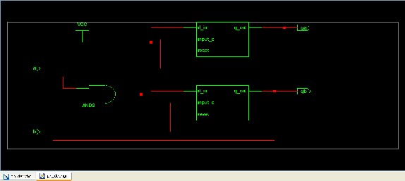
Fig. 3. RTL schematic of phase frequency detector
Fig. 4. CMOS implementation of Ring-VCO
IJSER © 2012
The research paper published by IJSER journal is about Mixed signal IC (CP-PLL) Testing scheme using a novel approach 5
ISSN 2229-5518
Fig. 5. RTL schematic of Ring VCO.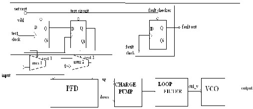
Fig. 6. Proposed BIST architecture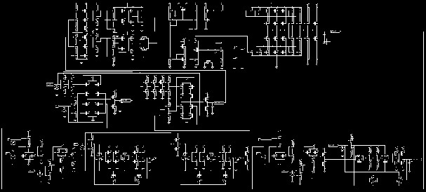
Fig. 7. CMOS implementation of the proposed BIST Architecture
IJSER © 2012
The research paper published by IJSER journal is about Mixed signal IC (CP-PLL) Testing scheme using a novel approach 6
ISSN 2229-5518
internal signals generated by the test-control circuit of the con trol unit. The output signal can observe and assess the test result directly. Notably, if fault out= ‗1‘ then the PLL is fault- free; otherwise, the fault out=‘0‘ if any block in PLL is faulty.
A model of the structural faults in the PLL, including a com- plete set of catastrophic faults, is established to demonstrate the efficiency of the proposed BIST structure in detecting structural faults throughout the PLL. Structural faults in the phase detector, the charge pump, the loop filter, the VCO, and/or the DBN are identified as follows:
1) gate-to-source short (GSS);
2) gate-to-drain short (GDS);
3) drain-to-source short (DSS);
4) Resistor short (RS);
5) Capacitance short (CS);
6) Gate open (GO);
7) Drain open (DO);
8) Source open (SO);
9) Resistor open (RO).
In this paper, low resistance (1) and high resistance (10 M)
frequently are used to simulate structural faults. Restated, a
transistor short is modeled using low resistance (1) between
the shorted terminals, and an open transistor is modeled as a large resistance (10 M) in series with the open terminals [8], [10], [11]. Notably, the gate-open is modeled by connecting the gate and the source, and also the gate and the drain of the transistor by a large resistance (10 M) and disconnecting the gate from other nodes. This could avoid the faulty transistor always in the off-state, which is not realistic model for a gate- open fault.
Avoltage sample-and-hold circuit commonly is used to main- tain the voltage for a particular period to measure the voltage at the output of the loop-filter. However, the sample-and-hold circuit occupies a large part of the die area on a chip. In this paper, the VCO is operated as a sample-and hold circuit using a simple average-count method to determine the voltage. This method requires no other circuit components, but merely re- quires an appropriate enable signal to operate the VCO. The output voltage of the loop-filter controls the oscillation fre- quency of VCO and the output of the VCO then is fed to the PFD, which acts as a frequency measuring device. Restated, the deviation of loop-filter output voltage from its normal val- ue changes the oscillation frequency of the VCO. Accordingly, when the proposed BIST structure is operated in the test mode, the oscillation frequency of the VCO reflects any faults in each PLL block. The VCO then measures the output fre- quency, and the final digital data is taken and stored by the fault-evaluation circuit. Significantly, the final test output in the proposed BIST structure can be evaluated directly.
The proposed BIST structure for PLL was fabricated using 125 nm CMOS 2p4m technology. Figure 7 illustrates the schematic diagram of the proposed BIST structure. Notably, all the ele- ments in the test circuits (the control unit, MUXs, and delay cells) were implemented by using the high performance CMOS circuits [12]–[14]. Notably, the locking time for the PLL without and with the added BIST circuits is 30 and 35ns, re- spectively. Thus, the characteristics of the PLL are less affected by the additional of the BIST circuits. The final digital data are determined from the output of the VCO and stored in the DFFs of the fault-evaluation circuit in the control unit. Addi- tionally, the results then are NORed by a NOR gate. To sum- marize, the NOR gate returns a logic 1 if PLL is fault free, and provides a logic 0 if any block in the PLL is faulty.
The total number of structural faults in the PLL block is 814.
All of the 814 faults were considered to evaluate the fault cov-
erage in each configuration and thus demonstrate the effec-
tiveness of the proposed BIST structure. Table 2 lists the final test outputs in the fault-free and some faulty cases, which in- clude the faults in each PLL block. Table 2 shows that the pro- posed BIST structure has high fault coverage (98.2%) results. The comparison of the fault coverage and area overhead with other techniques [5], [8] is also presented in Table 3. Notably, the definition of structural faults herein is similar to [8]. How- ever, only 395 faults were used and the phase detector cannot be tested in the testing process [8]. Thus, Table 3 indicates good performance of the proposed BIST structure which can be applied to provide a low-cost and highly effective BIST solu- tion for detecting structural faults. Although this paper shows minimum area overhead with higher fault coverage, the pro- posed BIST structure has the disadvantage of lacking jitter measurement and breaking the loop to include MUXs in the PLL design stage. However, the additional delay created by the MUXs can be incorporated in the original loop characteris- tics. This insures that the PLL characteristics are not altered by adapting the BIST technique.
IJSER © 2012
The research paper published by IJSER journal is about Mixed signal IC (CP-PLL) Testing scheme using a novel approach 7
ISSN 2229-5518
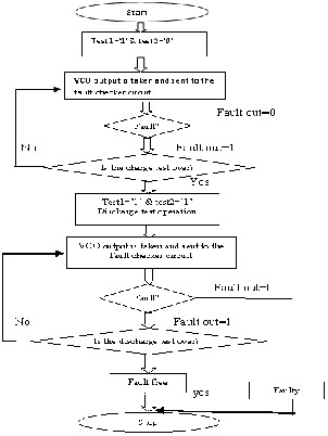
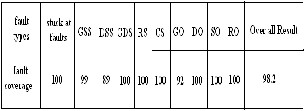
TABLE 3
COMPARISION W ITH OTHER PLL TESTING TECHNIQUES
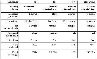
Fig. 8. Testing procedure
TABLE2
fault coverage results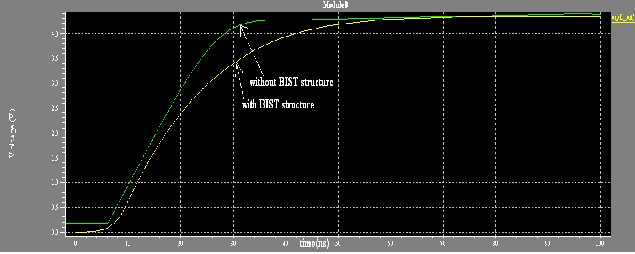
Fig. 9. step respons of the CP-PLL with and without BIST architecture.
existing blocks in the PLL, for example, the charge-pump,
VCO, as the stimulus generator and the measuring devices.
Physical chip design and fault simulation results reveal low
This paper presented a new BIST structure of the PLL in digi-
tal applications. This investigation attempted to implement a minimal area BIST structure for testing evaluation. To reduce the area overhead, the proposed BIST structure employs the
area overhead and high fault coverage. The test results clearly show promising applications where low-cost and effective PLL BIST is required with minimum area overheads. Briefly, this paper developed a low-cost practical on-chip BIST struc-
IJSER © 2012
The research paper published by IJSER journal is about Mixed signal IC (CP-PLL) Testing scheme using a novel approach 8
ISSN 2229-5518
ture for a PLL, owing to the BIST structure using the existing PLL blocks to perform the fault evaluation and the test output being purely digital.
[1] W. Dalal and D. Rosenthal, ―Measuring jitter of high speed data channels using under-sampling techniques,‖ in Proc. Int. Test Conf., Oct. 1998, pp. 814–818.
[2] B. R. Veillette and G. W. Roberts, ―On-chip measurement of the jitter transfer function of charge-pump phase-locked loops,‖ IEEE J. Solid- State Circuits, vol. 33, no. 3, pp. 483–491, Mar. 1998.
[3] K. A. Jenkin and J. P. Eckhardt, ―Measuring jitter and phase error in
microprocessor phase-locked loops,‖ IEEE Design Test Comput., vol.
17, no. 2, pp. 86–93, Apr.–Jun. 2000.
[4] K. Arabi and B. Kaminska, ―Oscillation Built-in Self Test (OBIST) scheme for functional and structural testing of analog and mixed - signal integrated circuits,‖ in Proc. Int. Test Conf., Nov. 1997, pp.
786–795.
[5] F. Azais, M. Renovell, Y. Bertrand, A. Ivanov, and S. Tabatabaei, ―A unified digital test technique for PLLs: catastrophic faults covered,‖ in IEEE Int. Mixed Signal Testing Workshop, 1999, pp. 269–292.
[6] I. Rayane, J. V. Medina, and M. Nicolaidis, ―A digital BIST for opera-
tional amplifiers embedded in mixed-signal circuits,‖ in IEEE VLSI
Test Symp., Apr. 1999, pp. 304–310.
[7] S. Sunter and A. Roy, ―BIST for phase-locked loops in digital appli-
cations,‖ in Proc. Int. Test Conf., Sep. 1999, pp. 532–540.
[8] S. Kim and M. Soma, ―An all-digital built-in self-test for high-speed phase-locked loops,‖ IEEE Trans. Circuits Syst. II: Analog Digit. Si g- nal Process., vol. 48, no. 2, pp. 141–150, Feb. 2001.
[9] ―Test evaluation and data on defect-oriented BIST architecture for
high-speed PLL,‖ in Proc. Int. Test Conf., Nov. 2001, pp. 830–837.
[10] J. L. Huang, C. Y. Pan, and K. T. Cheng, ―Specification back - propagation and its application to DC fault simulation for ana- log/mixed-signal circuits,‖ in Proc. VLSI Test Symp., Apr. 1999, pp.
220–225.
[11] M. Soma, ―Challenges in analog and mixed-signal fault models,‖
IEEE Circuit Devices Mag., vol. 12, pp. 16–19, Jan. 1996.
[12] J. L. Rossello and J. Segura, ―An analytical charge-based compact delay model for submicrometer CMOS inverters,‖ IEEE Trans. Cir- cuits Syst. I: Fundam. Theory Appl., vol. 51, no. 7, pp. 1301–1311, Jul.
2004.
[13] K. Runge and P. B. Thomas, ―5 Gbit/s 2:1 multiplexer fabricated in
0.35 _m CMOS and 3 Gbit/s 1:2 demultiplexer fabricated in 0.5 _m CMOS technology,‖ Electron. Lett., vol. 35, no. 19, pp. 1631–1633, Sep. 1999.
[14] M. Afghahi and J. Yuan, ―Double-edge-triggered D-flip-flops for highspeed CMOS circuits,‖ IEEE J. Solid-State Circuits, vol. 26, no. 8, pp. 1168–1170, Aug. 1991. W.-K. Chen, Linear Networks and Systems.
Belmont, Calif.: Wadsworth, pp. 123-135, 1993. (Book style)
IJSER © 2012