1.[7][8][9] . The same model has been used as a baseline while reducing the sub-threshold currents.
International Journal of Scientific & Engineering Research, Volume 3, Issue 5, May-2012 1
ISSN 2229-5518
Mitigating Techniques to Reduce Subthreshold
Currents in Submicron MOSFET’s
Akhil Ulhas Masurkar
Abstract— Scaling Transistors into the nano-meter regime has resulted in a dramatic increase in the MOS leakage currents . Threshold voltages have been scaled down to maintain the performance at reduced power supply voltages. Increased transistor leakages not only impact the overall power consumed by a CMOS system, but also reduce the margins available for design due to the strong relati onship between process variation and leakage power. Therefore it is essential for circuit designers to understand the components of leakage, sensitivity of leakge to different parameters, and leakage mitigating techniques in the nanometer technologies by designing accurate models of short channel devices and simulating the same using the available standard CAD tools. This paper provides an overview of t he mitigating techniques used during the fabrication of the MOSFET’s using SILVACO.
Index Terms— Scaling, Nanometer, Leakage, sensitivity, mitigating, simulating, fabrication, SILVACO
—————————— ——————————
Historically, VLSI designers have used circuit speed as the "performance" metric. Large gains, in terms of performance and silicon area, have been made for digital processors, micropro- cessors, DSPs (Digital Signal Processors), ASIC’s (Application Specific IC’s), etc. In general, "small area" and "high performance" are two conflicting constraints. The IC designer ’s activities have been involved in trading off these constraints. Power dis- sipation issue was not a design criterion but an afterthought [1][2]. In fact, power considerations have been the ultimate design criteria in special portable applications such as wrist- watches and pacemakers for a long time. The objective in these applications was minimum power for maximum battery life time. Recently power dissipation is becoming an important constraint in a design. Several reasons underlie the emerging of this issue.
Battery-powered systems such as laptop, notebook computers, electronic organizers, etc need an extended battery life. Many portable electronics use the rechargeable Nickel Cadmium (NiCd) batteries. Although the battery industry has been mak- ing efforts to develop batteries with higher energy capacity than that of NiCd, a strident increase does not seem imminent. The expected improvement of the energy density was 40% by the turn of the century [3][5]. With recent NiCd batteries, the energy density is around 20 Watt-hour / pound and the vol- tage is around 1.2 V. This means, for a notebook consuming a typical power of 10 Watts and using 1.5 pound of batteries, the time of operation between recharges is 3 hours. Even with the advanced battery technologies such as Nickel-Metal Hydride (Ni-MH) which provide large energy density characteristics (30 Watt-hour/pound), the life time of the battery is still low[4][6]. Since battery technology has offered a limited im- provement. Low-power design techniques are essential for portable devices.
The key challenge in reducing the leakage power is the Sub- threshold current. This can be reduced by proper choice of the substrate, appropriately doping the P or the N Substrate de- pending on PMOS or the NMOS being used, size of the chan-
nel implants and doping concentration of the channel im- plants. Optimizing these parameters will lead to reduction a reduction in the sub-threshold leakage for a given transistor technology.
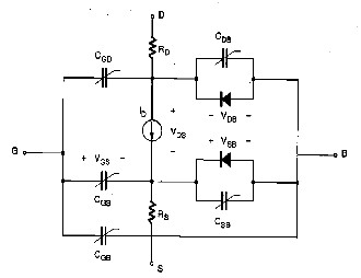
The equivalent circuit structure of the NMOS LEVEL 3 model, which is the default MOSFET model in SPICE, is shown in Fig
1.[7][8][9] . The same model has been used as a baseline while reducing the sub-threshold currents.
Figure 1. Equivalent MOS Model
![]()
![]()
Note that the voltage-controlled current source ![]() determines the steady-state current-voltage behaviour of the device, while the voltage controlled (nonlinear) capacitors connected be- tween the terminals represent the parasitic oxide-related and junction capacitances. The source-substrate and the drain- substrate junctions, which are reverse-biased under normal operating conditions, are represented by ideal diodes in this equivalent circuit. Finally, the parasitic source and drain resis- tances are represented by the resistors and , respective-
determines the steady-state current-voltage behaviour of the device, while the voltage controlled (nonlinear) capacitors connected be- tween the terminals represent the parasitic oxide-related and junction capacitances. The source-substrate and the drain- substrate junctions, which are reverse-biased under normal operating conditions, are represented by ideal diodes in this equivalent circuit. Finally, the parasitic source and drain resis- tances are represented by the resistors and , respective-
IJSER © 2012
The research paper published by IJSER journal is about Mitigating Techniques to Reduce Sub-threshold Currents in Submicron MOSFETs 2
ISSN 2229-5518
ly, connected between the drain current source and the respec- tive terminals.
The basic geometry of an MOS transistor can be described by specifying the nominal channel (gate) length L and the channel width W both of which are indicated on the element descrip- tion line. The channel width W is, by definition, the width of the area covered by the thin gate oxide. Note that the effective channel length ![]() is defined as the distance on the surface between the two (source and drain) diffusion regions. Thus, in order to find the effective channel length, the gate-source overlap distance and the gate-drain overlap distance must be subtracted from the nominal (mask) gate length specified on the device description line. The amount of gate overlap over the source and the drain can be specified by using the lateral diffusion coefficient
is defined as the distance on the surface between the two (source and drain) diffusion regions. Thus, in order to find the effective channel length, the gate-source overlap distance and the gate-drain overlap distance must be subtracted from the nominal (mask) gate length specified on the device description line. The amount of gate overlap over the source and the drain can be specified by using the lateral diffusion coefficient![]() .
.
For modelling p-channel MOS transistors, the direction of the dependent current source, the polarities of the terminal volt- ages, and the directions of the two diodes representing the source-substrate and the drain-substrate junctions must be reversed. Otherwise, the equations to be presented in the fol- lowing sections apply to p-channel MOSFETs as well.
The basic model implemented in SPICE calculates the drift current in the channel when the surface potential is equal to or larger than 2![]() that is in strong surface inversion. In reality, a significant concentration of electrons exists near the surface for
that is in strong surface inversion. In reality, a significant concentration of electrons exists near the surface for ![]() <
< ![]() , therefore, there is a channel current even when the surface is not in strong inversion. This is known as the sub- threshold current and is mainly due to diffusion between the source and the channel.
, therefore, there is a channel current even when the surface is not in strong inversion. This is known as the sub- threshold current and is mainly due to diffusion between the source and the channel.
A closer inspection of the ![]() -
-![]() curves of Fig (2) reveals that the current does not drop abruptly to 0 at
curves of Fig (2) reveals that the current does not drop abruptly to 0 at ![]() =
= ![]() . It becomes apparent that the MOS transistor is already partially conduct- ing for voltages below the threshold voltage. This effect is called sub-threshold or weak-inversion conduction [15][16][17]. The onset of strong inversion means that ample carriers are available for conduction, but by no means implies that no cur- rent at all can flow for gate-source voltages below
. It becomes apparent that the MOS transistor is already partially conduct- ing for voltages below the threshold voltage. This effect is called sub-threshold or weak-inversion conduction [15][16][17]. The onset of strong inversion means that ample carriers are available for conduction, but by no means implies that no cur- rent at all can flow for gate-source voltages below![]() , al- though the current levels are small under those conditions.
, al- though the current levels are small under those conditions.
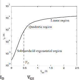
The transition from the on- to the off-condition is thus not abrupt, but gradual. When the ![]() versus
versus ![]() curve is drawn on a logarithmic scale as shown in Fig 3, confirms that the cur- rent does not drop to zero immediately for
curve is drawn on a logarithmic scale as shown in Fig 3, confirms that the cur- rent does not drop to zero immediately for ![]() <
< ![]() but actu- ally decays in an exponential fashion, similar to the operation of a bipolar transistor. In the absence of a conducting channel,
but actu- ally decays in an exponential fashion, similar to the operation of a bipolar transistor. In the absence of a conducting channel,
the n+ (source) - p (bulk) - n+ (drain) terminals actually form a parasitic bipolar transistor[11][12].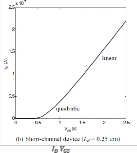
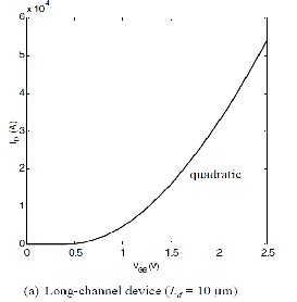
Figure 2. NMOS transistor - characteristic for long and short- channel devices (0.25µm CMOS technology).W/L = 1.5 for both transistors and ![]() = 2.5 V.
= 2.5 V.
The current in this region can be approximated by the expres- sion where ![]() and n are empirical parameters, with n≥1 and typically ranging around 1.5.
and n are empirical parameters, with n≥1 and typically ranging around 1.5.![]()
= ![]() ( 1-
( 1- ![]() ) (1)
) (1)
In most digital applications, the presence of sub threshold cur- rent is undesirable as it detracts from the ideal switch-like be- havior that we like to assume for the MOS transistor.
IJSER © 2012
The research paper published by IJSER journal is about Mitigating Techniques to Reduce Sub-threshold Currents in Submicron MOSFETs 3
ISSN 2229-5518
degraded by sub-threshold leakage. Achieving this in the presence of sub-threshold current requires a firm lower bound on the value of the threshold voltage of the device. For the
example of Fig 3, a slope of 89.5 mV/decade is observed (be- tween 0.2 and 0.4 V). This is equivalent to an n-factor of 1.49.
Figure 3. current versus (on logarithmic scale), showing the expo- nential characteristic of the sub-threshold region.
![]()
We would rather have the current drop as fast as possible once the gate-source voltage falls below . The (inverse) rate of decline of the current with respect to below ![]() hence is a quality measure of a device. It is often quantified by the slope factor S, which measures by how much
hence is a quality measure of a device. It is often quantified by the slope factor S, which measures by how much ![]() has to be reduced for the drain current to drop by a factor of 10. From (1) we find
has to be reduced for the drain current to drop by a factor of 10. From (1) we find
S = n![]() ln(10) (2) Where, n = 1 +
ln(10) (2) Where, n = 1 + ![]() (3)
(3)
Where ‘S’ is expressed in mV/decade. ![]() is the pinch off volt- age. For an ideal transistor with the sharpest possible roll-off, n=1 and (kT/q)ln(10) evaluates to 60 mV/decade at room tem- perature, which means that the sub-threshold current drops by a factor of 10 for a reduction in
is the pinch off volt- age. For an ideal transistor with the sharpest possible roll-off, n=1 and (kT/q)ln(10) evaluates to 60 mV/decade at room tem- perature, which means that the sub-threshold current drops by a factor of 10 for a reduction in ![]() of 60 mV.
of 60 mV.
Unfortunately, n is larger than 1 for actual devices and the current falls at a reduced rate (90 mV/decade for n = 1.5). The current roll-off is further affected in a negative sense by an increase in the operating temperature (most integrated circuits operate at temperatures considerably beyond room tempera- ture). The value of n is determined by the intrinsic device to- pology and structure [10][13]. Reducing its value hence re- quires a different process technology, such as silicon-on- insulator [6].
Sub-threshold current has some important repercussions. In general, we want the current through the transistor to be as close as possible to zero at ![]() = 0. This is especially important in the so-called dynamic circuits, which rely on the storage of charge on a capacitor and whose operation can be severely
= 0. This is especially important in the so-called dynamic circuits, which rely on the storage of charge on a capacitor and whose operation can be severely
Recent studies in the VLSI design area have proposed that the sub-threshold current can be reduced by
a. Changing the size of the drain and source regions.
b. Changing the doping concentrations of the source and drain implants depending on whether the MOS under fabrication is a PMOS or an NMOS.
c. Changing the doping concentrations of the Substrate used for fabrication.
d. Varying the Channel Length.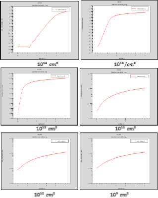
The following observations were made for a change in drain current in the sub-threshold region with variation in the dop- ing concentrations of the P-substrate (Considering NMOS us- ing SILVACO).
(a)8 x / (b)8 x
(c)8 x / (d)8 x /
(e)8 x / (f)8 x /
Figure 4. Variation in Sub-threshold current with change in the P- Substrate Doping concentrations
IJSER © 2012
The research paper published by IJSER journal is about Mitigating Techniques to Reduce Sub-threshold Currents in Submicron MOSFETs 4
ISSN 2229-5518
1. Initial orientation of the crystal is kept as [100]
2. P-well formation including masking off of the N-well is carried out at temp 1000 degree Celsius, diffusion time=30 minutes, dryo2 press=1.00. HCl=3
3. P-well Implant is carried out using boron dose=8e12 energy=100 pearsons, diffusion temp=950 time=100 wet ![]() HCl=3
HCl=3
4. N-well implant is carried out using the following
processes
a. diffusion time=50 temp=1000 t.rate=4.000 dry![]() press=0.10 HCl =3
press=0.10 HCl =3
b. diffusion time=220 temp=1200 nitro press=1
c. diffusion time=90 temp=1200 t.rate=-4.444 ni- tro press=1
5. Etching of oxide is done using sacrificially cleaning the oxide with diffusion time=20 temp=1000 dry![]() press=1 HCl=3
press=1 HCl=3
6. Gate oxide is then grown with diffusion time=11 temp=925 dry![]() press=1.00 hcl=3
press=1.00 hcl=3
7. ![]() (Threshold Voltage) adjust implant is carried out
(Threshold Voltage) adjust implant is carried out
using boron dose=9.5e11 with energy=10 pearson.
8. This then by a poly-silicon deposit to form the gate.
9. Excess poly-silicon is then removed using the method of Fermi compress with diffusion time=3minutes, temp=900 wet![]() press=1.0
press=1.0
10. Implant phosphor dose=3.0e12 energy=20 pearson
11. Deposit oxide thick
12. Implant arsenic dose=5.0e15 energy=50 pearson
13. Deposit aluminium thick=0.03
14. Etch aluminium
![]()
![]()
From the above results in Fig 5 it can be noted that, when the doping concentration was set to a value of 8 x /![]() at
at ![]() =0V, the off state current was equal to 1 x But the roll off slope is about 60mV/decade. This directly affects the threshold voltage and the threshold voltage increases to 1V. To mitigate this effect the P-substrate doping concentration was controlled to 8 x
=0V, the off state current was equal to 1 x But the roll off slope is about 60mV/decade. This directly affects the threshold voltage and the threshold voltage increases to 1V. To mitigate this effect the P-substrate doping concentration was controlled to 8 x ![]() /
/![]() and the n+ implant doping concen- tration was controlled to 3 x / . It was observed that the drain current at
and the n+ implant doping concen- tration was controlled to 3 x / . It was observed that the drain current at ![]() =0 increased to 1 x
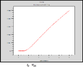
=0 increased to 1 x ![]() but the slope of the roll off increased to 125 mV/decade. The reduction in the threshold voltage was observed from 1V to 0.68V.
but the slope of the roll off increased to 125 mV/decade. The reduction in the threshold voltage was observed from 1V to 0.68V.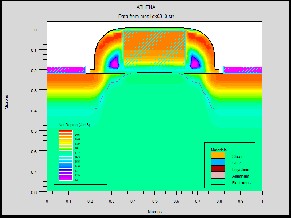
When the P-substrate and the n+ implant concentrations was set to the above values it was also observed that the gate to drain and gate to source overlaps were minimum (4nm), thus reducing the values of gate overlap parasitic capacitances. Also the shape of the source and drain implants have a shape close to a rectangular contour.
(5.a)Doping Profiles
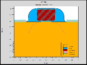
(5.b) Edges inside the MOS
(5.c) – curve (linear Scale)
IJSER © 2012
The research paper published by IJSER journal is about Mitigating Techniques to Reduce Sub-threshold Currents in Submicron MOSFETs 5
ISSN 2229-5518
(5.d) – curve (Logarithmic Scale)
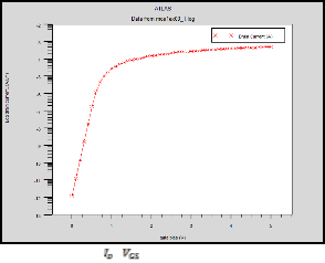
Figure 5. Optimized Results for minimum sub-threshold leakage
Since the majority of the transistors in a digital circuit are de- signed at the minimum channel length, the variation of the threshold voltage as a function of the length is almost uniform over the complete design, and is therefore not much of an is- sue except for the increased sub-threshold leakage currents. More troublesome is the DIBL, as this effect varies with the operating voltage. This is, for instance, a problem in dynamic memories, where the leakage current of a cell (being the sub- threshold current of the access transistor) becomes a function of the voltage on the data-line, which depends upon the ap- plied data patterns.
From the above results it can be observed that sub-threshold currents can be reduced to a minimum by keeping the P- substrate to N+ implants doping ratio to (8:3). By maintaining this doping ratio the threshold voltage can be controlled with- in the prescribed limits while still achieving low sub-threshold leakage currents and sharp roll off in the drain current below the value of the threshold voltage. Since the gate overlap capa- citances are very low, the parasitic capacitances reduce greatly and hence the transistor fabricated with the above doping ra- tio has reduced delays and can be used in high speed applica- tions.
I wish to acknowledge with deep gratitude the valuable guid- ance received from Prof. Swapnali Mahadik who encouraged me throughout this venture suggesting the necessary modifi- cations which has greatly improved the quality of the text. I am also thankful to Prof. Deepak V. Bhoir, Head of Electronics Engineering Department who gave necessary help from time to time as required.
[1] G.E. Moore, "Cramming more components onto integrated circuits," Electronics, vol.38, no. 8, April 19,
1965.
[2] C. Piguet, Are early computer architectures a source of ideas for low-power? Invited paper, Volta ’99, Como, Italy, March 4–5, 1999.
[3] C. Piguet, Histoire des ordinateurs. Invited paper at FTFC
’99, Paris, May 26–28, 1999, pp. 7–16.
[4] G. Baccarani, M. Wordeman, and R. Dennard,
‚Generalized Scaling Theory and ItsApplication to 1/4
Micrometer MOSFET Design,‛ IEEE Trans. Electron
Devices, ED-31(4): p. 452, 1984.
*5+ Prof. James Meindl and Dr. Richard Swanson ‚Design of Ion-Implanted MOSFETS with Very Small Physical Dimensions,‛ IEEE Journal of Solid-State Circuits, SC-9, pp. 256–258, 1972.
[6] P. Ko, ‚Approaches to Scaling,‛ in VLSI Electronics: Microstructure Science, vol. 18, chapter1, pp. 1–37, Academic Press, 1989.
*7+ L. Nagel, ‚SPICE2: a Computer Program to Simulate Semiconductor Circuits,‛ MemoERL-M520, Dept. Elect. And Computer Science, University of California at Berkeley, 1975.
[8] T. Thorpe, Computerized Circuit Analysis with SPICE,
John Wiley and Sons, 1992.
[9] Vladimirescu, The SPICE Book, John Wiley and Sons,
1993.G. Massobrio and P.
[10] Antognetti, Semiconductor Device Modelling with
SPICE, second edition, New York, NY: McGraw-Hill,
1993.
[11] J.E. Meyer, "MOS models and circuit simulation," RCA Review, 32, pp. 42-63, March 1971.
[12] M.C. Jeng, P.M. Lee, M.M. Kuo, P.K. Ko, and C. Hu, Theory, Algorithms, and User's Guide for BSIM and SCALP, Electronic Research Laboratory Memorandum, UCB/ERL M87/35, Berkeley, CA: University of California, 2008.
[13] B .J. Sheu, D.L. Scharfetter, P.K. Ko, and M.C. Jeng, "BSIM, Berkeley short-channel IGFET model," IEEE Journal of Solid-State Circuits, vol. SC-22, pp. 558-
566, 2005.
[14] P. Yang and P.K. Chatterjee, "SPICE modelling for small geometry MOSFET circuits," IEEE Transactions on Computer-Aided Design, vol. CAD-1, no. 4, pp.
169-182, 1999.
[15] S.-W. Lee and R.C. Rennick, "A compact IGFET
model-ASIM," IEEE Transactions on Computer-Aided
Design, vol. 7, no. 9, pp. 952-975, September 2001. [16] K. Lee, M. Shur, T.A. Fjeldly, and Y. Ytterdal,
Semiconductor Device Modelling for VLSI, Englewood
Cliffs, NJ: Prentice-Hall, Inc., 2009.
[17] Y. Cheng, M. Chan, K. Hui, M. Jeng, Z. Liu, J. Huang, K. Chen, R. Tu, P.K. Ko, C. Hu, BS1M3v3 Manual, Department of Electrical Engineering and Computer Science, University of California, Berkeley, 2010.
IJSER © 2012
The research paper published by IJSER journal is about Mitigating Techniques to Reduce Sub-threshold Currents in Submicron MOSFETs 6
ISSN 2229-5518

37 affiliated to the University of Mumbai, Maharashtra, India. He is currently pursuing his M.E. degree in Electronics Engi- neering from Fr. Conceicao Rodrigues College of Engineering, Mumbai – 50, affiliated to the University of Mumbai, Ma- harashtra, India. He is working as a lecturer in Department of Computer Engineering at Vidyalankar Institute of Technology, Mumbai-37, Maharashtra, India. He has 3 years of teaching experience at college level and his area of interest includes Microelectronics, VLSI and Digital System Design. He is a life member of ISTE and also a member of the IEEE.
IJSER © 2012