International Journal of Scientific & Engineering Research, Volume 4, Issue 12, December-2013 576
ISSN 2229-5518
Memory – based Encoding Algorithm for Minimization of Inductive Cross-Talk based on Off- Chip Data Transmission
Souvik Singha, G.K. Mahanti
Abstract— Inductive Cross-talk within IC Packaging is becoming a significant bottleneck in high speed inter chip communication. So the off-chip drivers typically source and sink 10 to 1000 drive internal loads. Thus simultaneously switching many off-chip drivers can cause large power (VDD) and ground current surges. These changes in current flow induce a voltage drop on the drivers’ local VDD rail and a voltage rise on the drivers’ local ground rail. The voltage drop is proportional to both the inductance of the VDD (ground) distribution network and the rate of change of the current flow (V= L * dl/dt).
In this work, we proposed a technique to avoid the inductive cross-talk in the inter-connect by encoding the data being transmitted off-chip. Bus encoding algorithms have been developed to overcome the capacitive cross-talk for on-chip buses, so the problem of on-chip capacitive cross-talk minimization for busses is very different from that of off-chip inductive cross-talk minimization. In this paper our approach also constructs cross-talk resistant CODEC algorithmically to utilize the memory-based CODEC solution.
Here we construct a set of equations which encoded the constraints that any legal vector sequence must satisfy to avoid supply bounce,
signal glitching, and signal edge speed degradation. From this set of equations, we construct a set of legal vector sequences for the bus. We use this set to find the largest effective size of the bus that can be achieved by encoding, for a given physical size of the bus.
Our experimental results show that the proposed encoding based techniques result in reduced supply bounce and signal degradation due to inductive cross-talk, closely matching the theoretical predictions. As a result the overall delay of the bus actually decreases even after the use of the encoding scheme.
Index Terms- Bus Encoding algorithm, Delay, Inductive Cross-talk, Interconnect, Off-chip bus.
IJ————S—————— E———————R———
1 INTRODUCTION
he limitation in package performance comes from the parasitic inductance and capacitance in the electrical interconnect [1, 3, 5] The parasitic inductance within IC packaging causes bounce on the power supply pins in addition to glitches and rise-time degradation on the single pins [1, 2, 10].In this work we give the mathematical analysis and the coding algorithm based on the reducing cross-talk for off-chip data transmission which we help on [1, 2]. This code is commonly referred minimization of inductive cross-talk for
Off-chip data transmission based on encoding.
The first step in creating the bus expansion encoder is to create a set of constraints equations. [1, 3, 7]. The constraint equations are written so that arbitrary transitions can be evaluated for noise limit violations. When the transition is evaluated using the constraint equations and violates one of the user-defined noise limits, the transition is flagged as illegal and is removed from the set of data sequences that are allowed to be riven through the package interconnects. Each of the possible off-chip transitions are evaluated against each of the
constraint equations. The inductance factors that effect signal
speed and integrity are as follows:-
————————————————
• Souvik Singha is doing his research work in National Institute of Technol- ogy, Durgapur, India, PH-09564620695. E-mail: singha.souvik@gmail.com
• G. K. Mahanti is presently a professor in the department of Electronics and
Communication Engineering, NIT, Durgapur, India, PH-09474600384. E-
mail: gautammahanti@yahoo.com
1.1 Supply Bounce Constraints
When a pin I in segment j is a VDD pin, it is required that the bounce magnitude due to the electrical parasitic in the package must not exceed the user-defined noise limit P supply. When the pin under evaluation is a VDD pin, a constraint equation is written to determine is any transitions that occur on the bus segment will result in a violation of P supply [1, 4, 6]. So the VDD pin in addition to any mutual inductive or capacitive coupling that occurs due to switching signals in adjacent pins. By multiplying the coupling magnitude by the transition value v j (which can be 0, 1, and -
1). When the pin under evaluation is a VSS pin, a constraint equation is written to determine if any transitions that occur on the bus segment will result in a violation of P gnd. Typically supply (VSS and VDD) pins are interspersed at regular intervals between signal pins. Every nth pin is a VSS or VDD. The supply bounce is proportional to the number of pins switching low or high. Ground bounce is expressed as:
Vbnc = L∑ (di / dt )
i
Where L is the self inductance of the VSS pin and ∑ (di / dt ) is
i
evaluated over the number of signal pins switching low.
1.2 Glitch Magnitude Constraints
When a pin I in segment j is a signal pin, it is required that the coupled voltage onto that pin does not exceed any of the user- defined noise limit for signal coupling [9,11,13] if the signal
pin is static (v j = 0)
then the glitch magnitude onto the victim
IJSER © 2013 http://www.ijser.org
International Journal of Scientific & Engineering Research, Volume 4, Issue 12, December-2013 577
ISSN 2229-5518
pin must not exceed P0. As in the constraint equations for supply bounce, the magnitude of the coupling contribution of any neighboring pin is multiplied by the transition value V (Which can be 0, 1, or -1) of the neighboring pin.
If a signal pin j is static, then a glitch may be induced in its voltage due to neighboring pins which switch.
This is governed by the expression
1.3 Switching Speed Constraints
When a signal is switching, its transition can be speed-up if the coupled voltage induced by its neighbor’s mutual inductance aids the transition. We would like that a signal is not slowed down (i.e. either speed-up, or un-integrated), in this transitions due to this effect we would like that when a signal j is rising (falling), the coupled voltage on this signal (equation 2) due to its neighbor’s transitions is zero or positive or negative. In this way, the transitions of signals are not slowed down due to inductive cross-talk.
1.4 Rise time and Fall time Degradation Constraints
When a signal pin I in segment j transitions from logic 0 and
Since the segments are arranged in a repetitive manner, the encoding obtained for segment will be valid for all K segments within the bus. So here we used the valid sequences to construct a legal transition between bus vectors. From this digraph, we construct a memory – based CODEC which is used during the bus data transfer.
3 CODING ALGORITHM
If an m- bit bus can be encoded using the legal transitions in
G, then there must exist a set of vertices VC ⊆ V , such that each Vs ∈ Vc has at least 2m out going edges e ( vs , vd ) (Including the self edge), such that the destination vertex vd ∈
Vc. so the cardinality of Vc is at least 2m. Now for any given graph G, we find m by the following given Algorithm.
Initially m is taken n-1 (when n is physical length of the bus). So the input of this Algorithm will be m and G. Here we first,
we find out- degree of each v (single vertices) ∈V. If the out-
degree of v is less than 2m then we assigned V ← V/v and
delete all out- going edges rooted at V as well as all in- coming
logic 1,
(v j = 1)
it is required that the coupled voltage onto
edges incident on v will continue this step until the graph is
that pin does not hinder its rise time.
In a similar manner, when a signal pin I in segment j
convergence. If after convergence the cardinality of v is greater
than 2m, We can construct a memory- based encoder using the
transitions from logic 1 to logic 0,
(v j = 1)
it is required that
legal transition of G. In this case the effective bus size can be
IJSER
i
the coupled voltage onto the pin does not hinder its fall time.

Bus encoding algorithms have been developed to overcome the capacitive cross-talk for on-chip buses [8, 9, 10]. However the problem of on-chip capacitive cross-talk minimization for busses is very different from that of Off-chip inductive cross- talk minimization. Although our approach also constructs cross-talk resistant to [1, 8, 9], we utilize memory based CODEC solution [14].
In this work we proposed systematic encoding scheme to reduce inductive cross-talk.
2 OUR APPROACH
Consider a bus consisting of k identical segments, each of width n. For any segment j, let j-1 represent the segment to its immediate right. Let us also denote the values if the n bits of
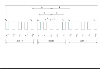
segment j as v j (0 ≤ i ≤ n −1) . Figure 1 shows an example of
a bus configuration with k = 3 and n = 5. So the signal- to- power ratio for this bus configuration is 5/2 shown in figure1. In general, when assigning package pins for an off- chip bus,
encoded in m. If m bit bus can not be encoded using G then
we decrement m, we repeat this until we find a value of m
such that the m bit bus can be encoded by G.
Algorithm 1: Testing if G(V,E)can encode an n-bit bus
Encode (m, G(V,E)) where m=n-1 & n = size of bus.
1. calculate the out degree ∀vi ∈V
2. degree = 1
3. Repeat steps 4 to 7 while degree=1
4. degree = 0
5. repeat steps 6 to 7 while each vi ∈V
6. If (out-degree of (vi < 2m) then
VDD and VSS pins are interspersed among the signal pins in a regular fashion. The over all bus arrangement consists of a
V ← V − vi
E ← E − e
(where V is the set of vertices)
(where e is the edges which is inci-
repetitive pattern of segments, each with their VDD and VSS pins in the same relative position within the segment which shown in figure 1.
In our approach, we write equations to encode the inductive cross talk constraints for all bits of the jth bus segment. The constraints are different for the signal, VDD and VSS pins. Depending of the number of neighboring pins whose mutual inductive effects we want to model, the constraint equations will include pins belonging to neighboring segments as well.
dent of vi )
Set degree=1
7. vi = vi + 1
8. Exit
IJSER © 2013 http://www.ijser.org
International Journal of Scientific & Engineering Research, Volume 4, Issue 12, December-2013 578
ISSN 2229-5518
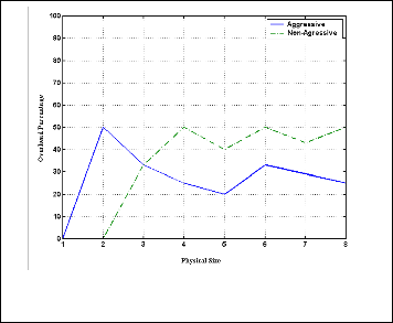
Fig 1: Example Bus Configuration
4 RESULT
In this work we encode an example bus configuration to avoid inductive crosstalk. The bus configuration is shown in figure1. Here we taken from Reference1, The first step consists of writing the constraint equations for every pin in the bus. In
5 CONCLUSION
Fig. 2 Encoding Efficiency
IJSER
this bus r =7 k =3 and α=7/2. For the inductive coupling with
a magnitude less than 0.08.This exercise yields 7 constraints
equations shown below. Note that these constraints have been simplified by removing terms with v j = 0
z
In this work, we present encoding techniques which can help a designer trade off cross- talk against area overhead. Our experimental results show that the proposed techniques result in reduced delay variation due to cross- talk. As a result in reduced delay of a bus actually decreases even after the use of
the encoding scheme. We also presented a technique to encode
1. v j =v DD

= (no of v j pins that are1) ≤ pbnc
2
Off-chip bus data to avoid inductive cross –talk effects. The technique involves writing constraints equations which express the user-specified bounds on the amount of edge
v j k v j
k v j
k v j
k v j p1
speed degradation, glitch magnitude, and supply bounce that
2. 1 = 1 ⇒
1( 2) +
2( 3) +
3( 4) +
4( 5) ≥
can be tolerated. In this paper, we have introduce the concept
v j k v j
k v j
k v j
k v j
p −1
of using data encoding to mitigate cross talk delay on buss
3. 1 = −1 ⇒
1( 2) +
2( 3) +
3( 4) +
4( 5) ≤
and we presented a theoretical framework for understanding crosstalk immune coding. In this work we proposed a bus
4.v j = 0 ⇒ − p
≤ k1(v j ) + k 2(v j ) + k 3(v j )
1 0 2 3 4
+ k 4(v j ) ≤ po
.
.
.
.
z
encoding technique to prevent cross talk delay for off-chip
data. We incorporate all these inductive cross-talk effects in a common Mathematical framework. We construct a set of legal vector sequences with respect to of legal vector sequences with respect to inductive cross-talk, and use these to develop a CODEC for inductive cross-talk avoidance.
Our experimental results show that the proposed encoding based techniques result in reduced supply bounce and signal degradation due to inductive cross-talk, closely matching the theoretical predictions. As a result the overall delay of the bus actually decreases even after the use of the encoding scheme.
17.v j = v ss

= (no of v j pins that are −1 ≤ pbnc
2
We found the value of the effective bus size n as a function of physical bus size m. the results are shown in figure 2, where we plot the bus size overhead (n-m / m) as a function of n.
REFERENCES
IJSER © 2013 http://www.ijser.org
International Journal of Scientific & Engineering Research, Volume 4, Issue 12, December-2013 579
ISSN 2229-5518
[1] Brock J. LaMeres, Sunil P.Khatri “Encoding-based Minimization of Inductive Cross-talk for off-chip Data Transmission ” Proceedings of the Design, Automation and Test in Europe Conference and Exhibi- tion(DATE’05) 1530-1591/05 IEEE.
[2] C.Chen and B. Curran, “Switching codes for delta-I noise reduction,” in IEEE Transactions of the 43rd IEEEMidwest SymposiumonCir- cuitsandSystems, vol.45, pp.1017-1021, Sept1996.
[3] The International Technology Roadmapfor Semiconductors.”
http://public.ltrs.net,2003.
[4] R. Tummalo, Fundamentals of Micro system Packaging. McGraw- Hill,2001.
[5] M.Miura, N.Hirano, Y.Hiruta, and T. Sudo, “Electrical characterization and
modeling of simultaneous switching noise for leadframe packages,” in
Proceedings of 45th Electronic Components and Technology Conference, pp.
857-846, May 1995.
[6] B.Young, “Return path inductance in measurements of package inductance matrixes,” in IEEETransmissions on Components, Packaging, and Manufacturing Technology, vol. 20, Feb 1997.1, Aug2000.
[7] N. Hirano, M. Miura, Y. Hiruta, and T. Sudo, “Characterization and reduction
of simultaneous switching noise for a multilayer package,”
[8] M. Lopez, J. Prince, and A. Cangellaris, “Influence of a floating plane on effective ground plane inductance in multilayer and coplanar packages,” in IEEE Transactions on Advanced Packaging, vol. 22, pp.182-188,May 1999.
[9] C. Duan, A. Tirumala, and S. Khatri, “Analysis and avoidance of cross-talk in
on-chip buses,” IEEE Symposium on High-Performance Interconnects (HOT Interconnects), pp.133-138,Aug 2001.
[10] C. Duan and S. khatri, “Exploiting crosstalk to speed up on-chip buses”,
Design Autamation and Test in Europe Conference, Feb 2004.
[11] B. Victorand K. Keutzer, “Bus encoding to prevent crosstalk delay,” in
Proceedings, IEEE/ACM International Conference on Computer Aided
Design, (SanJose, CA), pp.57 – 63, Nov 2001.
[12] M. Powell and T. Vijaykumar, “Pipeline damping: a micro architectural technique to reduce inductive noise in supply voltage,” in Proceedings of 30th International Symposium on Computer Architecture, pp.72-83, June 2003.
[13] E. Mejia-Motta, F. Sandoval-Ibarra, and J. Santana, “Design of cmos buffers using the settling time of the ground bounce voltage as a key parameter,” in Proceedings of 43rd IEEE Midwest Symposium on Circuits and Systems, vol.2, pp.718-72.
IJSER © 2013 http://www.ijser.org