
International Journal of Scientific & Engineering Research, Volume 3, Issue 11, November-2012 1
ISSN 2229-5518
Azharuddin Allamin Shaikh is currently pursuing degree program in electronics and telecommunication engineering in
SHIVAJI University, India , E-mail: shaikhazar52@gmail.com
Dattatraya Shashikant Shitole is currently pursuing degree program in electronics and telecommunication engineering in
SHIVAJI University, India, E-mail:shitole.datta@gmail.com
Abstract − There are many new emerging technologies in electronics and telecommunication but this paper focuses particularly about “MICRO- ELECTROMECHANICAL SYSTEM (MEMS) SENSOR
Purpose – To describe the development of micro-electromechanical system (MEMS) sensor technology, to consider its current use in sensing technology and to identify and discuss future technological trends and directions in today’s life of technology. Design/methodology/approach- We are poised in a revolution of microelectronics, which has dramatically reduced the cost and increased the capability of electronics because of its technology of very small devices. This has given much potential to prosper in the area of micro mechanics encompassing MEMS (Micro Electro Mechanical Systems). MEMS promises to revolutionize nearly every product category by bringing together silicon based microelectronics with micro machining technology, making possible the realization of complete systems on a chip. Commercial a pplications are inertial sensors, Power MEMS and RF switches. This technology is also used in industrial, consumer and auto motive marketing. Findings – This paper illustrates the greatly differing impacts sensing by MEMS technology. More recent developments are discussed which suggest strong market prospects for MEMS device and how important role the plays in today’s technology. Originality/value – This paper provides a technical and commercial insight into the applications of MEMS technology to physical and molecular sensors from the present day. It also identifies high growth areas for innovative developments in recent technologies
Index Terms—Automotive Sensor, Bulk micromachining, Biological Sensor, Chemical sensor, Electro Mechanical, High aspect ratio (HAR)
silicon micromachining, Micro Sensor, sensor, surface micromachining
Micro electromechanical systems (MEMS) is a technology of miniaturization that has been largely adopted from the integrated circuit (IC) industry and applied to the miniaturization of all systems not only electrical systems but also mechanical, optical, fluid, magnetic, etc.
1.1 Past: The origins of what we now know as micro- electromechanical system (MEMS) technology can arguably be traced back to 1 April 1954, when a paper by Smith (1954), then at the Bell Telephone Laboratories, was published in Physical Review. This described for the first time certain stress-sensitive effects in silicon and germanium termed piezo resistance. During the
mid-1950s, researchers were starting to investigate whether the same technologies that had yielded the transistor, which subsequently revolutionized the fledgling electronics industry, could be applied to sensors .These were crude by today’s standards (Figure 1) but in the early 1970s developments in micromachining, as it was then called and
improvements to silicon processing led to pressure sensors with non-planar diaphragm geometries which yielded superior performance These were arguably the first true MEMS sensors.
1.2 Present: Early polls indicate the automotive market for MEMS sensors and actuators grew nearly 16 percent in
2011 – great news considering the decline in sales due to the 2008 and 2009 recession.
1.3 Future: The success of the American auto industry is a contributing factor in the predictions that the market is expected to enter a fast growth phase that could top $3 billion and stretch into 2015.Because of the significant impact that MEMS can have on the commercial and defense markets, industry and the federal government have both taken a special interest in their development.
IJSER © 2012 http://www.ijser.org
International Journal of Scientific & Engineering Research, Volume 3, Issue 11, November-2012 2
ISSN 2229-5518
Industrial 2%
Consumer 3%
Medical 11%

Automotive 17%
Communicti ns
21%
Computer 26%
Microelectromechanical systems (MEMS) are small integrated devices or systems that combine electrical and mechanical components. They range in size from the sub micrometer (or sub micron) level to the millimeter level, and there can be any number, from a few to millions, in a
Predicted Contribution of MEMS technology in various field in 2013
A device used to measure a physical quantity (such as temperature) and convert it into an electronic signal of some kind (e.g a voltage), without modifying the environment. A sensor is a device which receives and responds to a signal. A sensor's sensitivity indicates how much the sensor's output changes when the measured quantity changes .Sensors are used in everyday objects such as touch-sensitive elevator buttons (tactile sensor) and lamps which dim or brighten by touching the base. There are also innumerable applications for sensors of which most people are never aware. Applications include cars, machines, aerospace, medicine, manufacturing and robotics.
MEMS or Micro Electro Mechanical Systems is a technique of combining Electrical and Mechanical components together on a chip, to produce a system of miniature dimensions .. By miniature, we mean dimensions less than the thickness of human hair.
particular system. MEMS extend the fabrication techniques developed for the integrated circuit industry to add mechanical elements such as beams, gears, diaphragms, and springs to devices.
These systems can sense, control, and activate mechanical processes on the micro scale, and function individually or in arrays to generate effects on the macro scale. The micro fabrication technology enables fabrication of large arrays of devices, which individually perform simple tasks, but in combination can accomplish complicated functions.Micro- Electro-Mechanical Systems, or MEMS, is a technology that in its most general form can be defined as miniaturized mechanical and electro-mechanical elements (i.e., devices and structures) that are made using the techniques of micro fabrication. The critical physical dimensions of MEMS devices can vary from well below one micron on the lower end of the dimensional spectrum, all the way to several millimeters. Likewise, the types of MEMS devices can vary from relatively simple structures having no moving elements, to extremely complex electromechanical systems with multiple moving elements under the control of integrated microelectronics. The one main criterion of MEMS is that there are at least some elements having some sort of mechanical functionality whether or not these elements can move. The term used to define MEMS varies in different parts of the world. In the United States they are predominantly called MEMS; while in some other parts of the world they are called “Microsystems Technology” or “micro-machined devices”.
IJSER © 2012 http://www.ijser.org
International Journal of Scientific & Engineering Research, Volume 3, Issue 11, November-2012 3
ISSN 2229-5518
The history of Si pressure sensors is widely recognized as
being representative of micro-sensor evolution. A micro sensor is a sensor that has at least one physical dimension at the sub-millimeter level, and today can be used to measure or describe an environment or physical condition such as acceleration, altitude, force, pressure, or temperature. Micromachining techniques have also enabled the development of micro actuators, which are devices that accept a data signal as an input, and then perform an action based on that signal as an output. Examples include micro valves for control of gas and liquid flows, optical switches and mirrors to redirect or modulate light beams, and micro pumps to develop positive fluid pressures. Sensors made are better than their using MEMS conventional counterparts because they are:
Smaller in size
Have lower power consumption
More sensitive to input variations
Cheaper due to mass production
Less invasive than larger devices.
Advances in IC technology and MEMS fabrication processes have enabled commercial MEMS devices that integrate micro sensors, micro actuators and microelectronic ICs, to deliver perception and control of the physical environment. These devices, also known as
'Microsystems' or 'smart sensors', are able to gather information from the environment by measuring mechanical, thermal, biological, chemical, optical, or magnetic phenomena. The IC then processes this information and directs the actuator(s) to respond by moving, positioning, regulating, pumping, or filtering. Any device or system can be deemed a MEMS device if it incorporates some form of MEMS-manufactured component. And there can be any number of MEMS devices within a particular Microsystem - ranging from just a few, to several million.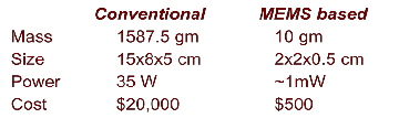
Demand for MEMS devices was initially driven by the government and military/defense sectors. More recently, a maturing of the semiconductor manufacturing processes associated with the microchips used within personal
computers, and the intersection with the huge requirement
in the automotive and consumer electronics sectors, has propelled MEMS sensors into the mainstream. The key MEMS sensors today are accelerometers, gyroscopes, and pressure sensors.
5.1 Materials:
Silicon
Silicon is the material used to create most integrated circuits used in consumer electronics in the modern world. The economies of scale, ready availability of cheap high- quality materials and ability to incorporate electronic functionality make silicon attractive for a wide variety of MEMS applications. Silicon also has significant advantages engendered through its material properties. In single crystal form, silicon is an almost perfect Hooke an material, meaning that when it is flexed there is virtually no hysteresis and hence almost no energy dissipation. As well as making for highly repeatable motion, this also makes silicon very reliable as it suffers very little fatigue and can have service lifetimes in the range of billions to trillions of cycles without breaking.
5.2 Polymers
Even though the electronics industry provides an economy of scale for the silicon industry, crystalline silicon is still a complex and relatively expensive material to produce. Polymers on the other hand can be produced in huge volumes, with a great variety of material characteristics. MEMS devices can be made from polymers by processes such as injection molding, embossing or stereo lithography and are especially well suited to micro fluidic applications such as disposable blood testing cartridges.
5.3 Metals
Metals can also be used to create MEMS elements. While metals do not have some of the advantages displayed by silicon in terms of mechanical properties, when used within their limitations, metals can exhibit very high degrees of reliability. Metals can be deposited by electroplating, evaporation, and sputtering processes. Commonly used metals include gold, nickel, aluminum, copper, chromium, titanium, tungsten, platinum, and silver.
IJSER © 2012 http://www.ijser.org
International Journal of Scientific & Engineering Research, Volume 3, Issue 11, November-2012 4
ISSN 2229-5518
5.4 Ceramics
![]()
The nitrides of silicon, aluminum and titanium as well as silicon carbide and other ceramics are increasingly applied in MEMS fabrication due to advantageous combinations of material properties. AlN crystallizes in the wurtzite structure and thus shows piezoelectric and piezoelectric properties enabling sensors, for instance, with sensitivity to normal and shear forces.[ Tin, on the other hand, exhibits a high electrical conductivity and large elastic modulus allowing to realize electrostatic MEMS actuation schemes with ultrathin membranes .Moreover, the high resistance of Tin against bio corrosion qualifies the material for applications in biogenic environments and in biosensors.
Basic Process
Deposition Patterning Etching
6.1 Deposition processes
One of the basic building blocks in MEMS processing is the ability to deposit thin films of material with a thickness anywhere between a few nanometers to about 100 micrometers.
6.2 Patterning
Patterning in MEMS is the transfer of a pattern into a material .Lithography in MEMS context is typically the transfer of a pattern into a photosensitive material by selective exposure to a radiation source such as light. A photosensitive material is a material that experiences a change in its physical properties when exposed to a radiation source. If a photosensitive material is selectively exposed to radiation (e.g. by masking some of the radiation) the pattern of the radiation on the material is
transferred to the material exposed, as the property of the exposed and unexposed regions differs.
6.3 Etching processes
There are two basic categories of etching processes: wet etching and dry etching. In the former, the material is dissolved when immersed in a chemical solution. In the latter, the material is sputtered or dissolved using reactive ions or a vapor phase etchant. for a somewhat dated overview of MEMS etching technologies.
7.1 Bulk micromachining:
Bulk micromachining is the oldest paradigm of silicon based MEMS. The whole thickness of a silicon wafer is used for building the micro-mechanical structures. Silicon is machined using various etching processes. Anodic bonding of glass plates or additional silicon wafers is used for adding features in the third dimension and for hermetic encapsulation. Bulk micromachining has been essential in enabling high performance pressure sensors and accelerometers that have changed the shape of the sensor industry in the 80's and 90's.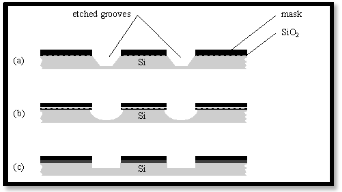
(Etched grooves using (a) anisotropic etchants, (b) isotropic etchants, (c) Reactive Ion Etching (RIE))
The differences between the various sorts of etching procedures. The thin layer visible between the photo resist and the silicon itself is silicon dioxide (SiO2). It serves as an etch mask for the Si etch, since its etch rate in most of the acidic etchants is considerably lower than that of Si, whereas photo resists do not stand up to the strong attack of most of the etchants. It is either a naturally grown oxide of approximately 20 Å (oxidation of silicon is nearly
IJSER © 2012 http://www.ijser.org
International Journal of Scientific & Engineering Research, Volume 3, Issue 11, November-2012 5
ISSN 2229-5518
unavoidable when exposed to an atmosphere containing
oxygen) or is thermally grown to a distinctive thickness.
7.2 Surface micromachining:
In contrast to the bulk micromachining described above, where three-dimensional structures are etched into the substrate wafer, surface micromachining consists of building them by layering thin films of new material onto the surface of the substrate. Usually, sacrificial spacer layers are used to create freestanding structures like air-bridges; after depositing such a sacrificial layer and patterning it using micro lithographic steps described above, the material for the final structure is deposited. Afterwards, the spacer layer is removed by an appropriate etchant, freeing the desired structure.
((a) Spacer layer deposition. (b) Pattering of the spacer layer. (c) Deposition of the microstructure layer. (d) Patterning of desired structure. (e) Stripping of the spacer layer resolves final structure.)
7.3 High aspect ratio (HAR) silicon micromachining:
Both bulk and surface silicon micromachining are used in the industrial production of sensors, ink-jet nozzles, and other devices. But in many cases the distinction between these two has diminished. A new etching technology, deep reactive-ion etching, has made it possible to combine good performance typical of bulk micromachining with comb structures and in-plane operation typical of surface micromachining. While it is common in surface micromachining to have structural layer thickness in the range of 2 µm, in HAR silicon micromachining the thickness can be from 10 to 100 µm. The materials
commonly used in HAR silicon micromachining are thick
polycrystalline silicon, known as epi-poly, and bonded silicon-on-insulator (SOI) wafers although processes for bulk silicon wafer also have been created (SCREAM). Bonding a second wafer by glass frit bonding, anodic bonding or alloy bonding is used to protect the MEMS structures. Integrated circuits are typically not combined with HAR silicon micromachining. The consensus of the industry at the moment seems to be that the flexibility and reduced process complexity obtained by having the two functions separated far outweighs the small penalty in packaging. A comparison of different high-aspect-ratio microstructure technologies can be found in the HARMST article.
There are many types of sensors now available in market such as,
Mechanical Sensors
Optical Sensors
Thermal Sensors
Chemical & Biological Sensors
8.1 Mechanical Sensors:
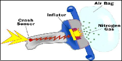
MEMS accelerometer is the one of the type of mechanical sensor. MEMS accelerometers have displaced conventional accelerometers for crash air-bag deployment systems in automobiles. The previous technology approach used several bulky accelerometers made of discrete components mounted in the front of the car with separate electronics near the air-bag and cost more than $50 per device. The car is equipped with airbags, means having a sensor “MEMS accelerometer “which is the IC (integrated circuit) small. The sensor works by detecting rapid-deceleration (slowing down too fast, CMIIW), who then ordered the system to inflate the airbag.
IJSER © 2012 http://www.ijser.org
International Journal of Scientific & Engineering Research, Volume 3, Issue 11, November-2012 6
ISSN 2229-5518
8.2 Optical Sensors:
A diaphragm-based interferometric fiber optical microelectromechanical system sensor with high sensitivity is designed and tested for on-line detection of the acoustic waves generated by partial discharges (PD) inside high- voltage power transformers. In principle, the sensor is made according to Fabric Perot interference, which is placed on a micro-machined rectangular silicon membrane as a pressure-sensitive element.
8.3 Thermal Sensors:
Thermal sensors detect the temperature & converts it into digital form. Developed through TI's (Texas Instrument) expertise in MEMS technology, the TMP006 is the first of a new class of ultra-small, low power, and low cost passive infrared temperature sensors. It has 90% lower power consumption and is more than 95% smaller than existing solutions, making contactless temperature measurement possible in completely new markets and applications.
8.4 Chemical & Biological Sensors:
Piezoelectric microelectromechanical systems (MEMS) resonant sensors, known for their excellent mass resolution, have been studied for many applications, including DNA hybridization, protein–legend interactions, and immunosensor development. They have also been explored for detecting antigens, organic gas, toxic ions, and explosives. Most piezoelectric MEMS resonant sensors are acoustic sensors (with specific coating layers) that enable selective and label-free detection of biological events in real time. These label-free technologies have recently garnered significant attention for their sensitive and quantitative multi-parameter analysis of biological systems.
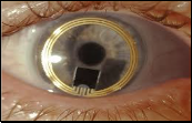
The soft contact lens like sensor, with its MEMS antenna
(golden rings), its MEMS sensor (silver ring close to the outer edge), and microprocessor
MEMS sensors have wide range of applications such as,
9.1 Automation:
MEMS technology finds applications in,
1. Airbag Systems
2. Vehicle Security Systems
3. Inertial Brake Lights
4. Headlight Leveling
5. Rollover Detection
6. Automatic Door Locks
7. Active Suspension
The automotive MEMS sensor market will reach new highs in 2012, leaving behind the ups and downs of 2009 and 2010 and the Japan Earthquake earlier this year. And the news gets much better beyond 2012: MEMS revenue from vehicle growth will jump 16% in 2012 to $2.31 billion, on its way to
$2.93B in 2015 (see Figure 1). This represents 9% growth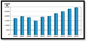
from 2010 to 2015.
Figure 1: Market for automotive MEMS sensors, 2006-2015 revenues in US $M. (Source: IHS supply) In 2015, although car production will reach a total of 98 million units and drive growth organically, the market "rocket" (i.e., mandates) will have exhausted their propellant by this stage -- and the sensor market therefore only grows at 5% in that year.
IJSER © 2012 http://www.ijser.org
International Journal of Scientific & Engineering Research, Volume 3, Issue 11, November-2012 7
ISSN 2229-5518
9.2 Medicine:
There are a wide variety of applications for MEMS in medicine. The first and by far the most successful application of MEMS in medicine (at least in terms of number of devices and market size) are MEMS pressure sensors, which have been in use for several decades. The market for these pressure sensors is extremely diverse and highly fragmented, with a few high-volume markets and many lower volume ones. Some of the applications of MEMS pressure sensors in medicine include:
1. MEMS pressure sensors are used to measure intrauterine pressure during birth. The device is housed in a catheter that is placed between the baby's head and the uterine wall. During delivery, the baby's blood pressure is monitored for problems during the mother's contractions.
2. MEMS pressure sensors are used in hospitals and ambulances as monitors of a patient’s vital signs, specifically the patient’s blood pressure and respiration.
3. The MEMS pressure sensors in respiratory monitoring are used in ventilators to monitor the patient’s breathing also in biconcavity laser.
9.3 Marine Science:
The advancement of MEMS technology has enable scientist to miniaturized sensors on a dimensional scale of microns
.Recently ,the achievements in mems technology helps to
adaption of new sensors into underwater .It helps to get more information about temperature ,pressure ,tidal & current velocity. The MEMS devices, in marine sensing may be attached to:
Ships, AUVs (Autonomous underwater vehicle), fixed sea
structure, sea bed.
MEMS sensors are also used to finding oil & gas reserves.
9.4 Military Operation:
1. An array of MEMS sensors spread on the ocean floor could detect the presence of enemy submarines.
2. MEMS sensors (pressure sensors, accelerometers etc.) are being used in anti-torpedo weapons on submarines and ships.
3. MEMS sensors in torpedoes are responsible for
detonating the torpedo at the right time.
4. Hitting the target in a crowded environment.
5. Prevent any premature explosion.
MEMS promises to be an effective technique of producing
sensors of high quality, at lower costs. Thus we can conclude that the MEMS can create a proactive computing world, connected computing nodes automatically, acquire and act on real-time data about a physical environment, helping to improve lives, promoting a better understanding of the world and enabling people to become more productive .
The author thanks the director of college “ANNASAHEB COLLEGE OF ENGG. & TECHNOLOGY” for financial support and also Dr. Shaila Subbaraman (professor at ADCET) Mrs. M. N. Chvan (asst. professor at ADCET) Mr. R. A. Jadhav (asst. professor at ADCET) For the technical assistance.
IJSER © 2012 http://www.ijser.org
International Journal of Scientific & Engineering Research, Volume 3, Issue 11, November-2012 8
ISSN 2229-5518
[1] S. AMPLE, PROC. MEMS 2011, PP. 100-103.
[2] ] A. B. STRACT AND S. AMPLE, TECH. DIGEST IEDM 2012, PP.
200-205.
[3] S. MART AND S. O. LUTION, J. MICROELECTROMECH. SYST., 23 (2006), PP. 300-315.
[4] B. Etter and A. P. Proach, The Gyro Handbook, 2nd ed. (Singer, 2001), pp. 400-401.
[5] MICRO MOLDED POLYMER FOR MICROFLUIDICS STRUCTURE (SRIKANTH RACHERLAR AND DENNIS LINGAD) (JOHN LEE, SJSU AND TREVOR NIBLOCK, CTO, ANALATOM, INC. SUNNYVALE, CA)
[6] Lyon.Bergveld, P. (1970), “Developments of an ion- sensitive solidstate device for neuro-physiological measurements”, IEEETransactions on Biomedical Engineering, Vol. 17, pp. 70-1.
[7] Lundstrom, K.I., Shiverman, M.S. and Svensson, C.M.
(1975), “A hydrogen-sensitive Pd-gate MOS transducer”,
Journal of Applied Physics, Vol. 46, pp. 3876-81.
IJSER © 2012 http://www.ijser.org