International Journal of Scientific & Engineering Research, Volume 3, Issue 5, May-2012 1
ISSN 2229-5518
Low Leakage Nanoscaled Body on Insulator
FinFET with Underlap
Sarika Bukkawar, Nisha Sarwade
Abstract—In this paper a Body over Insulator(BOI) FinFET structure in which channel region insulated from body by buried oxide with undoped underlap is studied . An extensive simulation study and analysis of the effect of underlaps on BOI FinFET has been performed using the TCAD SILVACO (DevEDIT(3D), ATLAS). The simulations have revealed that the BOI FinFET structures with underlaps are more efficient than conventional BOI FinFET as undoped underlap region reduces DIBL, leakage current(IOFF) and improves ION/IOFF ratio.
Index Terms—BOI(Body over Insulator)FinFET,BOX(Buried Oxide) DIBL(Drain Induced Barrier Lowering) ,leakage current, short-channel effects
(SCEs), silicon-on-insulator (SOI), subthreshold slope(S), underlap length (LUN ) .
—————————— ——————————
1 INTRODUCTION

THE miniaturization of the device dimensions has been historically used to improve the performance of bulk CMOS devices. The scaling of MOSFET dimensions has led to increased speed, high drivability, chips with increased functionality, and reduced cost [1], [2]. The era of bulk MOSFET, however, is nearing its end. The continuation of scaling of bulk MOSFET in the nanometer range (<65 nm) has become extremely difficult as the performance of bulk MOSFET is severely degraded by short channel effects (SCEs). The most important SCEs include drain-induced barrier lowering (DIBL), threshold voltage roll off problem, increase in gate leakage current, mobility degradation, etc. When the channel length shrinks, the gate control over the channel reduces due to various SCEs, such as DIBL, charge sharing, and subsurface punch through [3]. In such a scenario, the thin- film silicon-on-insulator (SOI)-based MOSFET looks set to become the next driver for CMOS scaling. SOI technology is capable of providing increased transistor speed, reduced power consumption, low leakage power, near-ideal isolation between devices, significant reduction in parasitic capacitance, and extended scalability. A significant reduction in SCEs and a steeper subthreshold slope are obtained in the thin-film SOI- based MOSFET. SOI has also become a substrate of choice for SOI-BiCMOS technology for efficient realization of system-on- chip[4,5,6]. However, the main problems associated with the SOI technology is self-heating and low breakdown voltage[7].The self heating manifests its effects in terms of degradation in reliability and in the overall performance of the device [8]For reducing self-heating effects, the use of some higher thermal conductivity materials such as amorphous carbon [10] and silicon nitride thin films [9] was proposed to replace the conventional buried oxide (BOX).
Sarika Bukkawar is currently pursuing masters degree program in Electronics engineering in University of Mumbai,India, PH-+91-9819669962. E-mail
:sarika_bukkawar@hotmail.com
Dr.Nisha Sarwade is professor in Electrical Engineering
Department in VJTI,Mumbai University, India,. E-mail:
nishasarwade@vjti.org.in
However, the fabrication of such SOI devices with high thermal conductivity layers needs complicated and costlier wafer bonding techniques, and the fabrication process is not advanced enough so far. The self-heating problems have been considerably reduced by partially insulated devices such as BOI FinFET and SDOI FinFET that uses silicon dioxide as partial BOX [11,12,23].The substrate offers heat dissipation path, thereby resulting in reduced self-heating while achieving high breakdown voltage. As the scaling is continued to nanoscale regime and equivalent distance between source and drain is decreased, the drain is more tightly coupled to channel region through gate insulator .Hence lateral electric field lines from drain reaches larger distance into the channel causing FIBL(Fringe Induced Barrier lowering)[13,14]. As the channel length of an FET is reduced, the drain potential begins to strongly influence the channel potential, leading to an inability to shut off the channel current with the gate. This closer proximity of drain to the channel give rise to higher SCE in high k MOS devices especially DIBL and subthreshold current[20]. Hence FET will have to accompanied by undoped underlap for minimizing drain potential over channel potential and thus reducing SCE [15, 17,19].
In this paper, BOI FinFET device with underlap is simulated
using the 3-D device simulator Devedit and Atlas of TCAD
Silvaco [22]. An advantage of BOI FinFET with underlap
serves both the purposes (i) dissipation of heat generated in the device as there is no insulation beneath S/D(ii)improving SCEs such as DIBL, leakage current etc This makes further scaling of the device possible. In this device, the BOX is present beneath the channel region. The undoped underlap with Si02 spacer has been used. The leakage current analysis of the device has shown that the BOI FinFET device with underlap has lower leakage current in comparison with the BOI FinFET device without underlap. Also DIBL is found to be reduced with increase in underlap length.
This paper is divided into four sections. Section 2 discusses the BOI FinFET structure which is been constructed in DevEDIT(3D), SILVACO. Section3 shows the simulation results and discussions have been given. Section 4 gives the conclusion.
IJSER © 2012
http://www.ijser.org
International Journal of Scientific & Engineering Research, Volume 3, Issue 5, May-2012 2
ISSN 2229-5518
2 DEVICE STRUCTURE
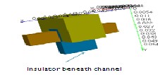
Fig1: buried oxide beneath the channel
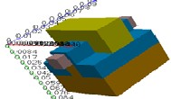
Fig2:BOI FinFET
Fig1 shows the insulating layer underneath the channel region of BOI FinFET with 30 nm gate length, 10 nm fin width and 15 nm fin height and the gate oxide thickness is universally 3 nm. Polysilicon is used as gate contact and Aluminium is used for the source and drain terminals. In the BOI FinFET, an insulation layer of 10 nm thickness and 20 nm height is introduced underneath the channel region. The channel region is uniformly doped with 1×10¹⁶/ cm3 p-type dopant. The source/drain (S/D) regions are doped with 1×10²⁰/ cm3 n-type dopant.
TABLE1
DEVICE DIMENSION (NM) AND OTHER PARAMETERS
suppress the leakage current between the source and drain. Better heat dissipation is also expected due to the absence of insulator under Source/Drain (S/D) region. Complete 3D simulations of the devices were performed using SILVACO DevEDIT (3D), Atlas TCAD software. A self-consistent Schrodinger-Poisson with Bohm Quantum Potential model (BQP) [22] is used for the simulations. The various models used in this study are fldmob, hcte, srh, fermi and bqp. The mobility model fldmob specifies that parallel electric field is used. The conventional drift-diffusion model of charge transport neglects non-local effects, such as velocity overshoot and reduced energy dependent impact ionization. These effects are incorporated in this study by using an energy balance model, which uses a higher order approximation of the Boltzmann Transport Equation. Since recombination effects are important, therefore, the concentration dependent Shockley–Read–Hall model (consrh) and Auger recombination model (auger) are activated in simulations. Similarly, we used Fermi-Dirac statistics for the simulation.
3.1 Short Channel Effects (SCEs)
The silicon fin thickness, gate oxide thickness, BOX thickness, junction depth, and channel length are the important parts of the device from an electrostatic point of view to control threshold voltage roll-off, DIBL, and subthreshold swing. The main SCEs are the threshold voltage roll-off due to charge sharing, the degradation of subthreshold swing(S), and the Drain induced barrier lowering(DIBL). These effects result in an increase in the OFF current (Ioff), decrease in threshold voltage (Vth) and the deterioration of the ON–OFF current ratio (Ion/Ioff). Electrostatic integrity relates both DIBL and threshold voltage roll-off SCE and describes the quality of electrostatic control of the channel by the gate .
3.2 Subthreshold Swing(S)
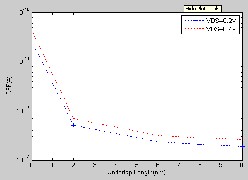
The subthreshold swing indicates how fast a device can react to a changing voltage level. This parameter is very important in gauging the speed of a device. Here, the variation of subthreshold swing of the simulated device against the underlap length is presented in fig-3. Subthreshold swing is calculated from ID-VGS plot by,
Subthreshold Swing=ΔVg(mV)/ΔlogId(decades) (1) Where ΔVg is change in gate voltage,Δ Id is change in drain current.
Subthreshold Swing S is found to be reduced by 36% at LUN
=10nm than BOI FinFET without underlap.
3 SIMULATION RESULTS
The schematic structure of the device under condition is given in the Fig. 2. In case of the BOI FinFET , a localized insulator is introduced at the bottom of the channel region which can
IJSER © 2012
http://www.ijser.org
International Journal of Scientific & Engineering Research, Volume 3, Issue 5, May-2012 3
ISSN 2229-5518
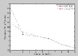
Fig 3:Effect of variation of underlap length on Subthreshold swing(S)
3.3 Threshold Voltage (Vth)
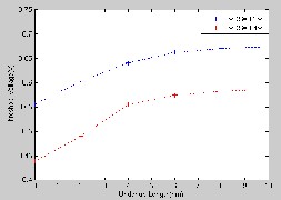
The continuation of scaling of bulk MOSFET in the nanometer range (<65 nm) has become extremely difficult as the performance of bulk MOSFET is severely degraded by short channel effects which includes threshold voltage roll off problem. As the underlap length increases control of drain over channel reduces resulting increase in threshold voltage. The variation of threshold voltage (Vth) with a change in underlap length is shown in Fig.4.Threshold voltage increases by 17% at LUN=10nm as that of without underlap. Hence problem of threshold voltage roll off can be resolved by changing underlap length. The required threshold voltage can be set by changing underlap Length.
Fig4: Effect of underlap in BOI FinFET on threshold voltage (Vth)
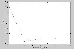
3.4 Leakage Current (IOFF)
The model for the subthreshold drain leakage current (VGS = 0)
is given by [6], [7], [27]
IOFF = μCG (W/L)(m − 1) [kBT/q ]2 exp[-qVT /mKBT] (3)
where m is the ideality factor, which can be expressed as
m = 1 + γ (C/CG) (4) Where CG is the gate-to-channel capacitance, C represents the
Channel-to-bulk capacitance. .
Leakage current in the device increases the power dissipation
unnecessarily and degrading the device lifetime. It is found that
leakage current is reduced by 99.27% at LUN=10nm than that of without underlap as shown in fig 5.
Fig5: Effect of variation of underlap length on IOFF
3.5 DIBL
The fundamental electrical limitation in VLSI will be the spacing of the surface diffusions that form p-n junctions. Reverse bias on one diffused junction creates a field pattern that can lower the potential barrier separating it from an adjacent diffused junction. When this barrier lowering is large enough, the adjacent diffusion behaves as a source, resulting in an unwanted current path. But in BOI FinFET with increased underlap length DIBL is found to be reduced by 25%as shown in fig- 6.
Fig 6:Effect of variation of underlap length on DIBL
3.6 Drain Current (ION)
Drain current is found to be reduced by 56% at LUN=10nm than that of without underlap as shown in fig-7 .
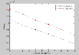
Fig7: Effect of variation of underlap length on ION
IJSER © 2012
http://www.ijser.org
International Journal of Scientific & Engineering Research, Volume 3, Issue 5, May-2012 4
ISSN 2229-5518
3.7 ION/IOFF
The ratio ION/IOFF is also found to be increased by 89% at
LUN=10nm than that of without underlap as shown in fig-8.
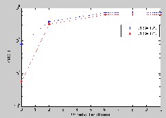
Fig8: Effect of variation of underlap length on ION/IOFF
4 CONCLUSION:
A 3-D simulation of BOI FinFET device with underlap has been performed. The incorporation of underlap with BOI FinFET device has resulted in a significant improvement in SCEs, particularly DIBL reduces by 25%, leakage current reduces by 99% and ION/IOFF increases by 89%.The reduction in leakage current reduces power dissipation when device is in off condition. This avoids heating, increases lifetime and ultimately the reliability of the device.
REFERENCES
[1] Leland Chang, YANG-KYU Daewon,,Pushkar Ranade,Shiying Xiong,,Jeffery Bokor,Chenming Hu,and Tsu-Jaeking, ―Extremely Scaled Silicon Nano-CMOS Devices‖ proceedings of the IEEE Vol.91,No.11,Nov2003
[2] Edward J. Nowak, Ingo Aller, Thomas Ludwig, Keunwoo Kim,
Rajiv V. Joshi, Ching-Te Chuang, Kerry Bernstein, and Ruchir Puri, ―Turning
Silicon On Its Edge‖ I EEE circuits & devices magazine Jan/Feb 2004,pp-20-31
[3] RONALD R. TROUTMAN , ―VLSI Limitations from Drain-induced Barrier Lowering‖ IEEE Solid –State Circuit Journal of Solid State Circuit Vol-SC-14, No. 2, April 1979 pp-383-390
[4] Mirko Poljaka, Vladimir Jovanovićb and Tomislav Suligoj, ―Technological
constrains of bulk FinFET structure in comparison with SOI FinFET‖ ISDRS 2007,
December 12-14, 2007
[5]S.L.Partridge,―Silicon-on-insulator technolog‖ IEE Proceedings , Vol. 133, Pt. I, No. 3, JUNE 1986
[6] K. K. Young, ―Short-channel effects in fully depleted SOI MOSFETs,‖ IEEE Trans. Electron Devices, vol. 36, no. 2, pp. 399–402, Feb. 1989.
[7] M. J. Kumar and A. A. Orouji, ―Investigation of a new modified source/ drain for diminished self-heating effects in nanoscale MOSFETs using computer simulation,‖ Phys. E, vol. 33, no. 1, pp. 134–138, Jun. 2006.
[8] C. Fiegna, Y. Yang, E. Sangiorgi, and A. G. O’Neill, ―Analysis of selfheating
effects in ultrathin-body SOI MOSFETs by device simulation,‖ IEEE Trans. Electron
Devices, vol. 55, no. 1, pp. 233–244, Jan. 2008.
[9] J. Roig, D. Flores, M. Vellvehi, J. Rebollo, and J. Millan, ―Reduction of self-heating
on SOIM devices,‖ Microelectron. Reliab., vol. 42, no. 1, pp. 61–66, Jan. 2002.
[10] Z. R. Song, Y. H. Yu, C. L. Li, S. C. Zou, F. M. Zhang, and X. Wang,―Tetrahedral
amorphous-carbon thin films of silicon-on-insulator application,‖Appl. Phys. Lett.,
vol. 80, no. 5, pp. 743–747, Feb. 2002.
[11] Jia Liu, Zhijiong Luo, Haizhou Yin, Huilong Zhu, Hefei Wang, Feng
Yuan, ―Low Leakage Bulk Silicon Substrate Based SDOI FINFETs‖ IEEE 978-
1-4244-5798- 2010
[12] Sajad A. Loan, S. Qureshi, andS. Sundar Kumar Iyer, ― A Novel Partial- Ground-Plane-Based MOSFET onSelective Buried Oxide: 2-D Simulation Study‖ IEEE Transactions on Electron Devices VOL. 57, NO. 3, MARCH
2010,pp 671-680
[13] Nihar R. Mohapatra, Madhav P. Desai and V. Ramgopal Rao,
―Detailed Analysis of FIBL in MOS Transistors with High-K Gate Dielectrics‖ Proceedings of the 16th International Conference on VLSI Design (VLSI’03) [14] G.C.-F. Yeap, S. Krishnan and Ming-Ren Lin,―Fringing-induced barrier lowering (FIBL) in sub-100nm MOSFETs with high-/(gate dielectrics‖ Electronics Letters 28th May 1998 Vol. 34 No. I 1pp-1150-1152
[15] Angada B. Sachid, C. R. Manoj, Dinesh K. Sharma, and V. Ramgopal Rao,
―Gate Fringe-Induced Barrier Lowering in Underlap FinFET Structures and
Its Optimization.‖ IEEE Electron Device letters , Vol. 29, No. 1, January
2008,pp-128-130
[16] Bing-Yue Tsui and Li-Feng Chin, ―A Comprehensive Study on the FIBL
of Nanoscale MOSFETs‖ IEEE Transaction on Electron Devices Vol. 51, No.
10, October 2004,pp-1733-1735
[17] Gaurav Saini, Ashwani K Rana, Pankaj Kr. Pal, Sunil Jadav,―Leakage Behavior of Underlap FinFET Structure: A Simulation Study‖ Int’l Conf. on Computer & Communication Technology | ICCCT’10 |pp-302-305
[18] Angada B. Sachid, Roswald Francis, Maryam Shojaei Baghini, Dinesh K.
Sharma, Karl-Heinz Bach, Reinhard Mahnkopf, V. Ramgopal Rao, ―Sub-20 nm Gate Length FinFET Design: Can High-κ Spacers Make a Difference?‖ [19]Vishal Trivedi, Jerry G. Fossum, and Murshed M. Chowdhury,―Nanoscale FinFETs With Gate-Source/Drain Underlap‖ IEEE electron Devices, VOL. 52, NO. 1, JANUARY 2005,pp-56-62
[20]Nihar R. Mohapatra, Madhav P. Desai, Siva G. Narendra, andV. Ramgopal Rao,―The Effect of High-K Gate Dielectrics on Deep Submicrometer CMOS Device and Circuit Performance‖ IEEE Transaction on Electron Devices, VOL. 49, NO. 5, MAY 2002,pp-826-831
[21]Tamara Rudenko, Valeria Kilchytska, Nadine Collaert, S. De Gendt,,Rita
Rooyackers, Malgorzhata Jurczak, and Denis Flandre ―Specific Features of the Capacitance and Mobility Behaviors in FinFET Structures‖ Proceedings of ESSDERC, Grenoble, France, 2005,pp-85-88
[22]Silvaco, Atlas User’s Manual, chapter 13. California, USA.
[23] Ashfaqul Anwar, Imran Hossain’ ―Comparative Numerical Simulation of a Nanoscaled Body on Insulator FinFET‖ ,PROC. 27th INTERNATIONAL CONFERENCE ON MICROELECTRONICS(MIEL 2010), NIŠ, SERBIA, 16-
19 MAY, 2010 ,pp 413-416
IJSER © 2012
http://www.ijser.org