International Journal of Scientific & Engineering Research, Volume 3, Issue 11, November-2012 1
ISSN 2229-5518
Low Voltage Low Power High Speed Flash ADC
with Multiplexer based code converter
Prasadh Teppala, K. Praveen Kumar, Ch. Praveen Kumar
Abstract— This paper presents a low voltage low power high speed flash analog-to-digital converter (ADC). The proposed flash ADC is pipelined using track and hold circuit and at the input and output latches of the code converter. A new digital code converter has been introduced using multiplexer based code (MBC) converter. The results show considerable improvement in the ADC delay. Power consumption is also reduced to great extent. Further noticeable power consumption reduction achieved for the flash ADC with the introduction of MBC converter operates at different low voltage levels. The ADC is designed in 130nm CMOS technology.
—————————— ——————————
The major considerations in designing ADCs on system- on-chip (SoC) are low power, low voltage and high speed. Recent high speed ADCs [1-3 ] have been reported to improve conversion speed by time interleaving, averaging termination, interpolating and folding etc.. But still achieving the speed greater than 2 giga samples per second (GSPS) is one of the major challenges in ADCs.
The Flash ADC conventionally contains resistor ladder circuit, comparator and code converter. Resistor ladder circuit is mainly to generate reference voltages. Because of high power consumption of resistors, TIQ comparator [4-6] and QV comparator [7, 8] are introduced to generate reference voltages and to generate the thermometer code by comparing the input voltage with the reference voltages. Code converter is used for converting the thermometer code to binary code.
In designing the high speed Flash ADCs, the code converter plays an important role in achieving speeds of the order of GSPS. ROM encoder [1-3] and fat-free encoder [9] are mostly used as code converters, but these converters convert thermometer code into the 1-out-of-n code and then into binary code. Because of the two steps of conversion, the ROM encoder and fat-free encoder give comparatively high propagation delay of the order of ns [8]. This paper presents a flash ADC using multiplexer based code converter [10] which directly converts the thermometer code into binary code in single step and run smoothly at the operating voltages less than 1.2 V.
————————————————
Prasadh Teppala, M.Tech in Digital Systems is a Asst. Professor at department of Electronics and Communication Engineering, GITAM University, Hyderabad Campus, India, PH-+918879168930.
K. Praveen Kumar, M.Tech in Digital Systems is a Asst. Professor at
department of Electronics and Communication Engineering, GITAM
University, Hyderabad Campus, India, PH-+919849414342
E-mail: kpraveen @gitam.ed.
Ch. Praveen Kumar, M.Tech in Digital Systems is a Asst. Professor at
department of Electronics and Communication Engineering, GITAM
University, Hyderabad Campus, India, PH-+919676143432
E-mail: cpk @gitam.edu
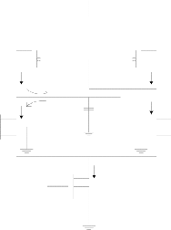
The proposed flash ADC consists of the Track and Hold circuit at the input followed by Quantum Voltage (QV) comparator, input latch, code converter and output latch. Its block diagram is given in Fig. 1. It is designed to consume low power at the operating voltage of 1.2 V. It works even on
1.1 V and 1.0 V also on the same sampling speed of 2.5 GSPS. It is pipelined by clocking at the input of Track and hold circuit and at the input and output latches of code converter. It takes one clock cycle for data conversion. The pipelining provides the proper functioning of the ADC and also reduces jitter due to clocking.
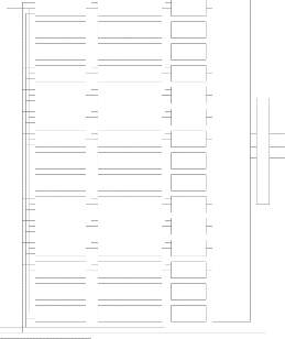
The architecture of the 4-bit flash ADC is shown in the Fig.
2. The 15 T/H circuits determine the signal offset and signal
amplitude to comparator. The 15 cascaded differential
comparators to produce the thermometer code by comparing
the T/H output with the internal reference voltages. The
MBC converter converts the thermometer code into binary
code in single step.
The Track and Hold circuit [8] is shown in the Fig. 3. It uses current mode dual array structure. Dual array structure improves the data throughput of the Flash ADC. The dynamic range of the Track and Hold circuit can be varied by varying the widths of the transistors T3 and T4, capacitance (C0) and the current source. The dynamic range of the Track and Hold circuit is 0.4 V and in the range of 0.4 V-0.8 V. The Track and Hold circuit in Flash ADC is mainly to provide signal offset voltage and signal amplitude to the comparator.
IJSER © 2012 http://www.ijser.org
International Journal of Scientific & Engineering Research, Volume 3, Issue 11, November-2012 2
ISSN 2229-5518
The schematic of the Quantum Voltage (QV) comparator is shown in the Fig. 4. By varying the sizes of the transistors Q3 and Q4 the internal reference voltages can be generated
Binary
VDD

Analog
S Ignal
Track and
Hold
+
Level Shifter
QV
comparator
Input
Latch
Code
Converter
Output
Latch
output
V1
Q1 Q2
clock
clock
0.2ns 0.2ns
I1 I2
i
V OUT
i
I3 C1 I4
Fig. 1. Block diagram of the Flash ADC.
![]()
![]()
V3 V4
INPUT
CLOCK CLOCK B
TRACK AND HOLD
TRACK AND HOLD
TRACK AND HOLD
TRACK AND HOLD
TRACK AND HOLD
TRACK AND HOLD
TRACK AND HOLD
TRACK AND HOLD
TRACK AND HOLD
TRACK AND HOLD
TRACK AND HOLD
TRACK AND HOLD
TRACK AND HOLD
TRACK AND HOLD
TRACK AND HOLD
DIFFERENTIAL COMPARATOR
DIFFERENTIAL COMPARATOR
DIFFERENTIAL COMPARATOR
DIFFERENTIAL COMPARATOR
DIFFERENTIAL COMPARATOR
DIFFERENTIAL COMPARATOR
DIFFERENTIAL COMPARATOR
DIFFERENTIAL COMPARATOR
DIFFERENTIAL COMPARATOR
DIFFERENTIAL COMPARATOR
DIFFERENTIAL COMPARATOR
DIFFERENTIAL COMPARATOR
DIFFERENTIAL COMPARATOR
DIFFERENTIAL COMPARATOR
DIFFERENTIAL COMPARATOR
LATCH LATCH LATCH LATCH LATCH
M LATCH B
C
LATCH
C
O LATCH N V
E LATCH R
T
LATCH E R
LATCH LATCH LATCH LATCH LATCH
O U T
P BIT3
U
T BIT2
L BIT1
A
T BIT0
C H E S
Q3 Q4
V2
I5
Vb
Q5
Fig. 4. The schematic of the QV comparator.
Here W3 and W4 are the widths of the transistors and Vtn, Vref (i), V4 , V2 are threshold voltage of nMOS, reference voltage of ith comparator, reference voltage and voltage at current source respectively.
By recursive simulation, widths of the transistors Q3 and Q4 obtained for the reference voltages which is deviating max 0.023 % by the ideal value. Therefore the differential nonlinearity is almost equal to zero.
The schematic of the latch is shown in Fig. 5. Here the![]()
![]()
VBIAS 0.2 ns DELAY
![]()
0.2 ns DELAY
latch is used for dual purpose. One is clocking and another one for improving the signal level. The transmission gates
Fig. 2. Architecture of the 4-bit flash ADC.
VDD
are used for clocking and the gain booster is used to achieve the full logic level at the input of a code converter.![]()
Current source

VOUT
V input
V clock V clock

T3
VDD
T1 T2
CK M1
M3
V OUT
VDD
V IN
C0
Current source
CK M4
M2
T4
CK
Fig. 3. The schematic of the T/H circuit.
by using the equation (1).
CK
Fig. 5. The schematic of the Latch.
W
2
(Vref (i) V2 Vtn )
(1)![]()
![]()
4 =
W3
(V4 V2 Vtn )
IJSER © 2012 http://www.ijser.org
International Journal of Scientific & Engineering Research, Volume 3, Issue 11, November-2012 3
ISSN 2229-5518
i
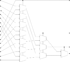
15 X3
14 1
13 0
12 1
11 0
10 1
9 0
8 1
X2
7 0
1
6 1 0
5 0
1
4 1 0 X1
3 0 1
1 X0
2 1 0
0
1 0
operates at the voltages of 1.2 V, 1.1 V and 1.0 V and at a
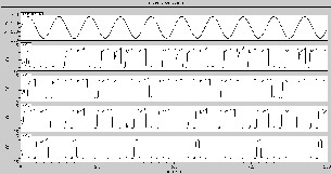
speed of 2.5 GSPS. The simulation results of the 4-bit proposed flash ADC at input frequencies 125MHz, 250MHz,
500MHz, and 1000MHz are shown in Figs 7-10 respectively.
From the simulations it is clear that the flash ADC has the input bandwidth of the 1GHz hence proposed flash ADC can be used for RF signal processing. The performance and comparison of the 4-bit flash ADC is shown in Table 1 and Table 2.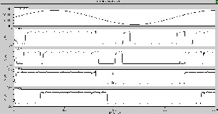
q 0 1 2 3
Fig. 6. The schematic of the Multiplexer based code converter.
The pipelined flash ADC employs the Multiplexer based code converter (MBC) which is shown in Fig. 6. Due to the regular structure, the MBC converter can be expanded to more than 4-bit.
The main idea behind the multiplexer based decoder is that, in 2n-1 bit thermometer code the middle bit i.e. 2n-1 level is always equal to the MSB of the n-bit binary code. This
2n-1 level of the thermometer code separates the thermometer code into two partial thermometer codes. If 2n-
1 level is low then select the lower partial thermometer code and the middle bit is equal to (MSB-1)st bit of n-bit binary code else select the upper partial thermometer code and the middle bit is equal to (MSB-1)st bit of n-bit binary code From this (MSB-1)st bit of n-bit binary code determined. In the similar way remaining bits of the binary code can be found. This process continued up to the LSB remains.
The critical delay (all paths are having the same delay) of
the code converter is only three multiplexer delay (three transistor’s delay) where as in DCVSPG decoder, the critical delay is of five XOR gates each having two transistors. The code converter converts the thermometer code into binary code in single step only. Due to the simple structure and less hardware the power consumption of the code converter reduces significantly.
The proposed flash ADC is designed and simulated in
Cadence EDA tool. It uses the IBM 130nm technology which
Fig. 7. Simulation results of ADC at 125 MHz input.
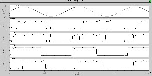
Fig. 8. Simulation results of ADC at 250 MHz input.
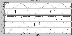
Fig. 9. Simulation results of ADC at 500MHz input.
IJSER © 2012 http://www.ijser.org
International Journal of Scientific & Engineering Research, Volume 3, Issue 11, November-2012 4
ISSN 2229-5518
VLSB | 0.025V | 0.025V | 0.025V |
Fig. 10. Simulation results of ADC at 1000 MHz input.
TABEL 1
Comparison of the flash ADCs
From the Table 1, the delay of the MBC converter is 69.14
% lesser than the DCVSPG decoder. The power consumption
of the 4-bit flash ADC (MBC converter) at 1.2 V is 5.12 % lesser than the flash ADC (DCVSPG decoder). And also the active area of the flash ADC (MBC converter) also reduced by 27.61 % in compared to the flash ADC (DCVSPG decoder).
From the Table 2, it clear that the power consumption of the proposed flash ADC (MBC converter) at 1.1 V, 1.0 V is reduced by 18.93 %, 35.88 % with respect to the proposed flash ADC (MBC converter) at 1.2 V respectively.
This paper presents a Low voltage Low power High Speed Flash ADC with the MBC converter for high-speed flash CMOS ADCs. The MBC converter improves the speed and power consumption in comparison with the flash ADC (DCVSPG decoder). It is clear from the simulation results that the delay of the MBC converter is improved by 69.14 %, power consumption of the proposed flash ADC is reduced by 5.12 %. The flash ADC (DCVSPG decoder) is working up to power supply of 1.2 V only, however the proposed flash ADC (MBC converter) runs smoothly at power supplies 1.1V and 1.0 V with reduced power consumption with the same data conversion rate of 2.5 GSPS, hence it is suitable for portable devices.
ADC
type
Table 2

Comparison of the flash ADCs (MBC)
Proposed Flash ADC(MBC)
1.2 V 1.1 V 1.0 V
[1] X. Jiang, Z. Wang amd M.F Chang, “A 2GS/s 6-b ADC in 0.18µm
9-13, Feb. 2003
[2] M. Choi and A. Abidi, “A 6-b 1.3 Gsamples/s A/D converter in0.35
Resolut ion
Sampli ng Rate
4 BIT 4 BIT 4 BIT
2.5GSPS 2.5GSPS 2.5 GSPS
μm CMOS,” IEEE Journal of Solid-State Circuits, Vol. 36, pp. 1847-
1858, Dec. 2001.
in 0.18 µm CMOS using Averaging Termination,”
IEEEJournal of Solid-State Circuits, Vol. 37, No. 12, December 2002.
Power 3.3125m
W
2.6853m
W
2.1240m
W
[4] J.Yoo, D. Lee, K. Choi, and A. Tangel. "Future-Ready Ultrafast 8bit
CMOS ADC for System-on-Chip Applications", In IEEE
Decode r
0.2015ns 0.292 ns 0.513ns
International ASIC/SOC Conference, pages 455-459, 2001.
Converter for System -on-Chip Applications”, In IEEE Computer
delay | Society Workshop on VLSl, pp. 135-139, April 2001. | ||||
Active | 31.17 μm2 | 31.17 | 31.17 | [6] | J. Yoo, K. Choi, D. Lee. “Comparator Generation and Selection for |
Area | μm2 | μm2 | Highly Linear CMOS Flash Analog-to-Digital Converter,” Journal of | ||
Dynam ic range | 0.4V-0.8V | 0.4V- 0.8V | 0.4V- 0.8V | [7] | Analog Integrated Circuits and Signal Processing, 35(2-3), pp. 179-187, J. Yoo, K. Choi, and J. Ghaznavi, “Quantum voltage comparatorfor |
0.07 μm flash A/D converters,” Proceedings of the IEEEComputer
IJSER © 2012 http://www.ijser.org
International Journal of Scientific & Engineering Research, Volume 3, Issue 11, November-2012 5
ISSN 2229-5518
Society Annual Symposium on VLSI, pp. 20-21, Feb.2003
[8] M.Wang, C I H Chen, S.Radhakrishnan, “Low-Power 4-b 2.5 GSPS Pipelined Flash Analog-to-Digital Converter in 130nm”, in IEEE Instrumentation and measurement,pp1064-73, June 2007.
[9] D. Lee, J. Yoo, K. Choi and J. Ghaznavi, “Fat-tree encoder design for
ultra-high speed flash analog-to-digital converters,” IEEE Midwest
Symposium on Circuits and Systems, 2002.
[10] E. Säll and M. Vesterbacka, “A multiplexer based decoder for flash analog-to-digital converters,” Proc. TENCON 2004, Nov. 21-24, 2004.
IJSER © 2012 http://www.ijser.org