International Journal of Scientific & Engineering Research Volume 2, Issue 12, December 2011 1
ISSN 2229-5518
Influence of Growth Temperature on the
Photoluminescence of Zinc Oxide Nanomaterial
Alvin Noe Ladines, Gil Nonato Santos
Abstract— We report the synthesis of zinc oxide nanomaterials on glass substrate through the non-catalytic horizontal vapor phase growth method. The optimal growth conditions in the growth of a particular kind of nanomaterial were determined. Nanobelts with average width of
200 nm were grown when the growth temperature was set at 1200°C and 1000°C. Nanowires with mean diameter of 100 nm were
dominant at growth temperatures of 800°C and 600°C. Shorter growth time resulted in the formation of needle-like structures which are 2 micrometers in length. Increasing the growth time corresponded to the growth of nanowires with average length of 10 micrometers. XRD measurements showed that the synthesized nanostructures have a hexagonal wurtzite structure with growth preference in the (001), (101) and (10-1) directions. The room-temperature photoluminescence spectra showed an intense ultraviolet emission (UV) at 3.26 eV with weak emissions in the visible light regime. The strong UV emission can be attributed to the recombination of free excitons though an exciton- exciton collision process. Meanwhile, the deep level emissions are caused by oxygen vacancies in ZnO and the emission results in the recombination of the photogenarated hole with an electron occupying the oxygen vacancy. It is proposed that growth mechanism involved in the formation of ZnO nanostructures is the vapor-solid process because no catalyst was used.
Index Terms— nanomaterials, photoluminescense, scanning electron microscopy, thermal evaporation, vapor-solid growth, X-ray diffraction, zinc oxide
1 INTRODUCTION
—————————— ——————————
ECENTLY, there has been a growing interest in zinc oxide nanomaterials because of their excellent optolectronic [1], piezoelectric [2], gas sensing [3] and lasing properties [4]. Different nanostructures of ZnO including nanowires, nano- belts, nanohelixes, nanocages, needle-like and comb-like struc- tures can be synthesized though various methods reported in literature. The noncentral wurtzite crystal structure of ZnO and the tetrahedrally coordinated ZnO4 unit result in its aniso- tropic piezoelectric properties. Rapid growth in the <0001>,
<0110> and <2110> directions and polar surface-induced phe- nomena result in the formation of the diverse group of nano- structures of ZnO. [5]
ZnO is a wide band gap semiconductor with a direct band
gap of 3.36 eV and a large excitation binding energy of 60 meV
thus exhibiting near-ultraviolet emission and transparent con-
ductivity. Also, ZnO is biologically-safe and biocompatible so
it can be used for biomedical applications. [4] Various me-
thods were developed to synthesize ZnO nanostructures which includes basic erosion method [6], electrodeposition [7],
thermal oxidation [8,], vapor epitaxy method [9], chemical vapor deposition [10], vapor-liquid-solid process [11], simple evaporation method [12-14], solution phase reaction [15] and flame synthesis [16] among others.
Horizontal vapor phase crystal growth (HVPCG) method was developed as an economical alternative to the evaporation method. It is a simple and efficient method of growing high purity nanomaterials without using any gas as catalyst. More importantly, it is eco-friendly since the process of evaporation does not interfere with the environment. [17]
————————————————
Alvin Noe Ladines, Master of Science in Physics, Lecturer, De La Salle
University-Manila, Philippines. E-mail: noe_interactive@yahoo.com
Gil Nonato C. Santos, Doctor of Philosophy in Materials Science, Profes-
sor, De La Salle University-Manila, Philippines. E-mail:
santosg@dlsu.edu.ph
In this paper, we report the synthesis of ZnO nanomate- rials through the non-catalytic HVPCG method. The surface morphology, stoichiometry and photoluminescence of the grown nanomaterials will be investigated.
2 PROCEDURE
Approximately 35 mg of ZnO powder obtained from Sigma- Aldrich Singapore Pte Ltd is loaded into an ultrasonically- cleaned quartz tube with length of 220 mm, outer diameter of
11 mm and inner diameter of 8.5 mm. The quartz tube contain- ing the source material is connected to a high-vacuum system via a flange equipped with a metal to glass quick-connect. The tube is then sealed using an appropriate mixture of liquefied petroleum gas and oxygen when the pressure is in the order of
10-6 torr. The sealed quartz tube is then set on a horizontal
tube furnace which is programmed at a certain growth tem-
perature and dwell time. The growth temperatures were set at
600°C, 800°C, 1000°C and 1200°C while the dwell time was
adjusted from two hours to six hours in two-hour increments.
A temperature gradient of about 300°C between the end of the quartz tube containing the source material and the growth site
was maintained. This would cause the ZnO powder at the hotter end to evaporate and condense at the colder part of the quartz tube. At the end of the baking period, the furnace is allowed to cool down to room temperature naturally. The na- nomaterials that are deposited on the walls of the quartz tube are subjected to SEM (JEOL 5310 series) and EDX analysis (Ox- ford with Link Isis) without further treatments. XRD (Bede Scientific D3 System) and PL (Olympus BX series) measure- ments were also done on the samples after the exact growth site of the nanomaterials was established using SEM.
IJSER © 2011
http://www.ijser.org
International Journal of Scientific & Engineering Research, Volume 2, Issue 12, December-2011 2
ISSN 2229-5518
3 RESULTS AND DISCUSSION
3.1 Growth temperature dependence
Figure 1 shows the SEM images of various nanostructures prepared at different growth temperatures with constant dwell time of two hours. Unreacted ZnO powder and web-like nanostructures at the initial stage of formation are observed at a growth temperature of 600°C. Randomly-oriented nanowires with typical dimension of less than 100 nm were grown at
800°C as evident in the SEM image. Needle-like structures with average diameter of 120 nm were synthesized at 1000°C. When the growth temperature is increased to 1200°C, blade- like structures with widths of approximately 200 nm are formed. It can be inferred from the SEM images that the di- mensions of the synthesized nanostructures is dependent on the growth temperature.
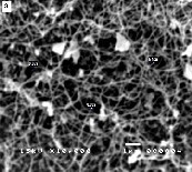
At relatively lower temperatures the growth is preferred along a single direction such that one-dimensional nanostruc- tures i.e., nanowebs and nanowires are formed. With suffi- ciently higher energy of reaction, growth preference in this direction terminates and growth in other directions appears. This explains why nanostructures such as nanoblades and needle-like structures are observed at higher growth tempera-
amount of ZnO vapor that migrate toward the colder region inside the tube and subsequently condensing on the walls re- sulting in the observed nanostructures. The one-dimensional nanostructures that were formed are approximately of the same size which suggests that dwell time does not contribute to the growth of ZnO nanostructures in other directions.
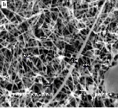
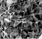
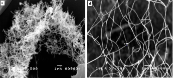
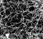
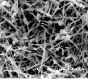
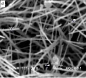
Figure 2: SEM images of ZnO nanostructures synthesized at different dwell times: (a) 2 hours (b) 4 hours (c) 6 hours (d) 8 hours
3.3 X-ray diffraction

XRD measurements were conducted to assess the crystal structure of the as-synthesized nanomaterials. Figure 3 presents the representative XRD spectra of the grown nano- materials compared with other studies [18]. A prominent peak
from the
(101) plane can be observed while peaks from the
(002), (101) and (103) planes were also detected. This polycrys-
talline nature of the samples can be verified from the SEM im- ages. Determination of the lattice parameters was not success-
ful owing to the relatively weak intensity of the XRD peaks of the nanostructures.
tures.
Figure 1: SEM images of ZnO nanostructures synthesized at different growth temperatures: (a) 600oC (b) 800oC (c) 1000oC (d) 1200oC
3.2 Dwell time dependence
Figure 2 compares the SEM images of ZnO nanostructures synthesized at a growth temperature of 1200°C but at different dwell times. The synthesized nanomaterials feature a width which ranges from 100 nm to 200 nm and length which ex- tends from 5 microns to 10 microns. It can be noted that a longer growth time resulted in the formation of longer nano- structures. Moreover, an increase in the amount of the grown nanomaterials was observed as the growth time is extended. An increase in growth time corresponds to an increase in the
3.4 Photoluminescence

The representative room temperature PL spectra of the syn- thesized nanomaterials are shown in Figure 24-26. The spectra exhibited intense ultraviolet (UV) peak at approximately 380 nm and weak emissions in the visible light regime. It has been shown in previous studies that the UV peak can be attributed to the recombination of free excitons through an exciton- exciton collision process [19]. The band gap energy Eg can be
computed from Eg hc and is equal to 3.26 eV, close to the band gap of ZnO. Meanwhile, the deep level emissions are
caused by singly ionized oxygen vacancy in ZnO and the emission results from the radiative recombination of photoge- nerated hole with an electron occupying the oxygen vacan- cy[20].
IJSER © 2011
http://www.ijser.org
International Journal of Scientific & Engineering Research, Volume 2, Issue 12, December-2011 3
ISSN 2229-5518
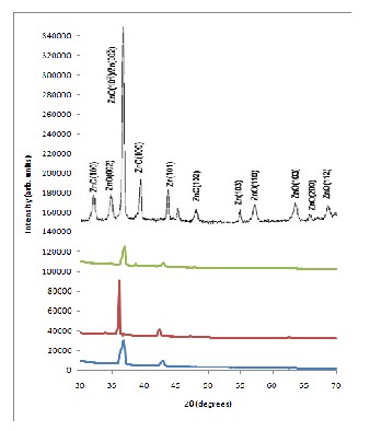
Figure 3: (a-c) Representative XRD spectra of the synthesized ZnO nanomaterials (d) XRD spectra of ZnO nanomaterials synthesized through thermal oxidation [18]
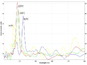
Figure 4: Representative PL spectra of ZnO nanomaterials
3.4 Proposed Growth Mechanism
The possible growth mechanism for the synthesis of ZnO na- nostructures is through the vapor-solid process (VS) because no metal catalyst was used in this study [5]. It is proposed that the synthesis process is divided into two stages; nucleation and growth. As the source material is heated, it dissociates into ZnO in the vapor phase and transfers into the colder sec-
tion of the tube guided by temperature gradient that exists along the length of the tube. The rough inner wall of the quartz tube, providing an energy barrier in the vapor trans- port is believed to be the site of condensation and subsequent nucleation of ZnO molecules. The growth process proceeds as more ZnO molecules pile up at the nucleus eventually form- ing the nanostructure. Due to the preferred growth orientation of ZnO in the c-axis, one-dimensional nanostructures are syn- thesized. Meanwhile, with sufficient amount of energy, growth in other directions also appears, thus nanostructures like nanobelts, nanoblades and nanorods are also formed. The absence of a patterned substrate led to the formation of nano- materials that do not have a single orientation.
4 CONCLUSION
Zinc oxide (ZnO) nanomaterials were successfully synthesized through the horizontal vapor phase growth method. The re- sults suggest that growth temperature and dwell time affect the structure of the ZnO nanomaterials. Various nanostruc- tures which include nanowires, nanoblades and needle-like nanostructures were formed when the growth conditions were adjusted. It was shown from the PL measurements that the synthesized nanomaterials have excellent optical property. The nanomaterials, therefore, offer a wide range of applica- tions in nanoscale optoelectronic devices.
ACKNOWLEDGMENT
The authors wish to thank the Department of Science and
Technology for the research grant.
REFERENCES
[1] Ahmad Umar, Kim S., Kim J., Park Y., Hahn Y. (2007).
Structural and Optical properties of single-crystalline ultra- violet-emitting needle-shaped ZnO nanowires. Materials Let- ters, 61, 4954-4958.
[2] Zhou J., Lao G., Gao P., Mai W., Hughes W., Deng S., Xu N., Wang Z. (2006). Nanowire as pico-gram balance at workplace atmosphere. Solid State Communication, 139,
222-226.
[3] Hsueh T., Hsu C., Chang S., Chen I. (2007). Laterally grown
ZnO nanowire ethanol gas sensors. Sensors and Actuators B,
126, 473-477.
[4] Wang Z.L. (2004). Nanostructures of Zinc Oxide. Materials
Today, 26-33.
[5] Kong X.Y. and Wang Z.L. (2003). Spontaneous Polarization of Induced Nanohelixes, Nanosprings, and Nanorings of Pie- zoelectric nanobelts. Nano Letters, 3, 1625-1631.
[6] Liu et.al., “Nanostructured ZnO films obtained by basic erosion method,” Applied Surface Science 252 pp 8668-
8672, 2005.
[7] Elias et.al., “Electrochemical deposition of ZnO nanowire
arrays with tailored dimensions,” Journal of Electroana-
lytic Chemistry, 2007.
[8] Bai et.al., “Fabrication of highly ordered and stepped ZnO
comb-like structures,” Applied Surface Science 253 pp
IJSER © 2011
http://www.ijser.org
International Journal of Scientific & Engineering Research, Volume 2, Issue 12, December-2011 4
ISSN 2229-5518
6835-6839, 2007.
[9] Song et.al. , “Vertical growth f ZnO nanowires on c-Al2O3
substrate by controlling ramping rate in a vapor-phase ep-
itaxy method,” Journal of Physics and Chemistry of Sol- ids, 2007.
[10] Li et.al., “Low temperature synthesis of novel ZnO nano- wire microspheres on Silicon substrate,” Rare Metals 26 pp 242-246, 2007.
[11] Yang et.al., “Photoluminescence and Raman analysis of ZnO nanowires deposited on Si (100) via Vapor-Liquid- Solid process,” Physica E 40 pp 920-923, 2008.
[12] Fang et.al., “The influence of growth temperature on ZnO
nanowires,” Materials Letters 62 pp 1092-1095, 2007.
[13] Umar et.al., “Structural and Optical properties of single-
crystalline ultraviolet-emitting needle-shaped ZnO nano-
wires,” Materials Letters 61 pp 4954-4958, 2007.
[14] Hsu et.al., “Ultraviolet photodetectors with low tempera-
ture synthesized vertical ZnO nanowires,” Chemical
Physics Letters 416 pp 75-78, 2005.
[15] Kao et.al ., “Low temperature solution and synthesis and
photoluminescence properties of ZnO nanowires,” Jour-
nal of Alloys and Compunds, 2007.
[16] Xu et.al., “Flame synthesis of zinc oxide nanowires,”
Chemical Physics Letters 449 175-181, 2007.
[17] Ngo, et.al., “Tin Oxide Nanomaterial through Vacuum
Deposition Technique,” Proceedings of the 9th DLSU-OU
Academic Research Workshop pp 104-107, 2007.
[18] Ren et.al. , “Catalyst-free synthesis of ZnO nanowire ar- rays on Zn substrate by low temperature thermal oxida-
tion,” Materials Letters 61 pp 666-670, 2006.
[19] Lyu S.C., Zhang Y., Ruh H., Lee H.J., Shim H.W., Suh E.K.,
Lee C.J. (2002). Chem. Phys. Lett., 363, 134.
[20] Vanheusden K., Warren W. L., Seager C.H., Tallant D.R.,
Voigt J.A., Gnade B.E. (1996). J Appl Phys., 79, 7983.
IJSER © 2011
http://www.ijser.org