International Journal of Scientific & Engineering Research, Volume 4, Issue 4, April-2013 421
ISSN 2229-5518
Improving RFID Tag Efficiency by QAM Backscatter Modulation
T.S. Ajitha#1, V.Bhanumathi#2
Abstract— Traditional passive UHF RFI D tags employ backscatter modulat ion to communicate data from memory or sensors on the tag to a rem otely located reader. When compared with binary am plitude shift keying (ASK) or phase shift keying (PSK) based RFID systems, which transmit 1 bit of data per symbol period, and thus 1 bit per on-chip clock oscillator period, tags em ploying vect or backscatter modulation can transmit m ore than 1 bit per sym bol period. This increases the data rat e for a given on-chip sym bol clock rate leading to reduced on-chip power consumption and extended read range. The perform ance of the backscatter uplink involves improvem ent in spectral efficiency and data rat e. The spectral efficiency is determined by the constellation choice used. By increasing the constellation order, spectral efficiency doubles but causes further power loss per bit. Hence a new m odulation scheme is proposed to balance the norm alized power loss per bit and the increased spectral efficiency. Here, a 16-QAM m odulation scheme with forward error control coding is proposed t o achieve the desired perform ance. Device-level simulation and m easurem ents of a sixteen-st ate quadrature amplitude modulated (16-QAM) modulator are provided for a passive t ag operating in the 850–950-MHz band. This modulat or transmits QAM at a symbol rat e of 200 kHz with a static power dissipation of only 115nW .
Keywords—Backscattering modulation, RFID, passive RF identification (RFID) tags, quadrat ure am plitude modulat ed (QAM)
backscatter, ultra-high-frequency (UHF) RFID.
—————————— ——————————
adio Frequency Identification, or RFID, is a technology that uses radio frequency communication to automatically identify, track and manage objects, people or animals. A backscattering radio-frequency
identification (RFID) system is generally composed of a reader, reader antennas, and tags. The backscattering RFID system is called passive when the tag does not carry an embedded battery but is activated by converting power from the reader illumination. On the other hand, a semipassive (or semiactive) backscattering tag has an internal battery to assist operation of the digital circuitry in the tag. The maximum communication range of passive RFID systems is determined by the range of either the forward power transfer link or the backward scattering link, the backward link range alone generally determines the maximum available range of semipassive backscattering RFID systems.
An RFID tag re-engineering conformal to the vision of sensing applications [1] is represented by the Wireless Identification and Sensing Platform (WISP) [2]. A sensor network using RFID components would, first and foremost, require integration of sensors that in turn, incurs significant new energy cost. Second, the sensor data is expected to be transferred to a central repository, requiring enhanced uplink rates and reliability compared to
the antenna loading [7]. The current industry standard - EPC Global Gen-2 specifies two binary encoding schemes, FM0 and
Miller sub-band coding, for the uplink, implemented with either two state amplitude shift keying (ASK) or phase shift keying (PSK), it was shown in [9] that a linear receiver for FM0 operating over two successive symbols achieves near-MLSE performance.
In the paper [8], demonstrates the use of load-dependent scattering to generate QAM backscatter with a simple modulator suitable for single-chip CMOS implementation. It shows that it is feasible to build backscatter systems supporting higher order constellations, e.g. 4-QAM or 8-QAM. However, improved spectral efficiency implies an energy cost. During backscatter modulation the tag’s impedance is intentionally mismatched, and hence the power harvested is reduced (compared to quiescent state). Denote the power harvested under conjugate matched conditions as Pmatch, the average power harvested during backscatter as Pavg, and information bits per symbol (C). To introduce the metric, the normalized power loss per information bit
Pmatch Pavg
present-day application of (one-time) reading of the EPC code. The poor tag sensitivity and power harvesting in passive tags limit the downlink range [3] and achievable link throughput.
Ploss
![]()
CPmatch
(1)
Hence uplink improvements will be key to future RFID systems.
During uplink and downlink communication, the reader’s radio frequency (RF) carrier wave energizes the RFID tag via power harvesting. Uplink communication occurs by modulating
The objective in this work is: to a) investigate ways to improve uplink spectral efficiency and b) to characterize the associated normalized power loss per bit and to reduce the static power consumption for the tag operation. Increasing the constellation order from binary signalling to 4-QAM doubles the spectral efficiency, but causes further power loss per bit. The
IJSER © 2013
International Journal of Scientific & Engineering Research, Volume 4, Issue 4, April-2013 422
ISSN 2229-5518
work investigates how the co-design of the QAM constellation geometry and forward error correction (FEC) may be used to balance the normalized power loss per bit and increased spectral efficiency. First establish an equivalent circuit model in Section 3 for the RFID tag in terms of a backscatter modulation design parameter that determines the trade-off between backscattered signal to the reader and the available power transferred to the tag. Section 4 provides information about the backscattered signal. Section 5, explore QAM constellation design such that the power loss during backscatter is minimized. Next, Section 6 provides demodulation in passive RFID. The latter exploits the advantage of asymmetric power harvesting in a 16-QAM constellation caused by backscatter modulation. The simulation results and quantitative evaluation are discussed in section 7.
Chakra borty, [3] presented how to maximize the uplink and downlink range of an RFID (passive tag) by optimal selection of modulation indices for Amplitude Shift Keying modulation. ASK based RFID systems can transmit only one bit of data per symbol period, and thus On-chip symbol clock rate is high. Hence the processing time has been increased and more power is harvested by the chip. Reynolds, in [8] proposed M-ary QAM backscatter technique by which tags transmit more than one data bit per symbol period, permitting tag designers to employ a lower power on-chip oscillator operating at a frequency equal to the (lower) symbol rate while maintaining the same data throughput as ASK or PSK. Park, and Yang, in [10] proposed an optimized ON/OFF states of the backscattered amplitude shift keying (ASK) modulator for the passive RF identification (RFID) tags by taking into account both the reader receiver sensitivity and tag antenna mismatch conditions. Iannacone, in [9] presented a set of design criteria for the RF section of passive transponders in the UHF and microwave frequency range, with the main objective of maximizing the operating range.
Despite the fact that many backscatter modulation scheme deliver good performances by providing efficient communication, there are still several problems that have not yet been solved satisfactorily. First, reduced data rate: one bit per symbol period; Second, high probability of error; Third, more power harvested and increased processing time. In this paper, a new coded modulation scheme to tradeoff the spectral efficiency with normalized power loss was proposed which provides a good solution to the above problems.
Passive and semi-passive RFID tags have desirable form factors with a low-power IC connected to external components such as the antenna. The IC integrates several different analog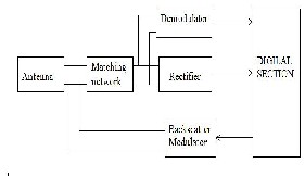
Figure 1.Passive RFID tag system.
A typical passive RFID system, as shown in Fig. 1, is comprised of the tag and the reader. The tag carries the data, while the reader interrogates and fetches the data from the tag. The interface for any application between the user and the RFID reader system should be provided in the server. However, the data transfer between the reader and tag is done using electromagnetic (EM) waves. In the passive RFID system, the reader should provide the tag with both the dc power for operation and the interrogation sequence since there is no embedded battery. The rectifier block in the tag harvests RF energy radiated from the reader and transfers it into dc power to support tag operation. The interrogation data are detected by the demodulator and analysed by the digital block. After the tag is invoked and interrogated by the reader, the response of the tag is returned as a backscattered RF signal during the CW period. In the passive RFID system, the power, harvested by the tag, directly determines the read/write (R/W) range or identification range between the reader and tag. The tags need to backscatter sufficient power to satisfy the reader sensitivity. This is determined from the maximum allowable bit error rate (BER). Thus, the power link between the RFID reader and tag needs to be investigated very carefully.
The RFID reader continues radiating RF signal to the tag. The radiated power is usually measured by effective isotropic radiated power (EIRP). The radiated power suffers a path loss, quantified using the Friis free-space formula. It is then received by the tag antenna. In the meantime, the RF power, reflected by the tag antenna, suffers the same attenuation as the radiated signal from the reader in the space and is detected by the reader. Taking the reader and tag antenna gain and effective area into consideration, the power available to the tag chip and power detected by the reader can be expressed, respectively, as follows:
1 2
![]()
![]()
. .
subsystems such as an AC-to-DC voltage converter (power
harvester), followed by voltage multiplier and the (data)
modulator/demodulator followed by the digital subsections,
Pavs EIRP Gr
. .G
4R 2 4 t
2
(2)
consisting of a low power microprocessor and a small amount of
. . 1
memory [10]. An impedance matching network placed between the antenna and IC attempts to maximize power transfer from the ambient to on-chip storage element. During backscatter operation the tag IC is the only active component. The IC modulates the![]()
![]()
Pdr Pbs Gt
. .G
4R 2 4 r
(3)
antenna’s load impedance, ZIC, via switching a variable impedance component within the tag IC. The mismatch between
the antenna’s impedance Rant and the IC’s impedance ZIC
decreases the power transfer from antenna to tag.
where Pavs , Pbs and Pdr are the RF power available at the tag
antenna, the RF power reradiated at the tag antenna, and the
power detected by the reader, respectively. Gr and Gt are the
IJSER © 2013
International Journal of Scientific & Engineering Research, Volume 4, Issue 4, April-2013 423
ISSN 2229-5518
gain of the reader antenna and the gain of the tag antenna. R is
the distance between the tag and reader. λ is the wave length.
is a purely reactive component jXmod. The combined impedance of the circuit in Eqn (6) is then
A Thevenin equivalent model, Fig. 2(a). for the antenna and IC consists of a voltage source VOC with the same frequency as the reader’s RF carrier ω, in series with the antenna represented by complex impedance Zant = Rant + jωLant. The RFID IC chip
Zmod
![]()
jRmod X mod
Rmod jX mod
R X 2 jX R 2
![]()
mod mod mod mod
impedance is assumed to have a capacitive component in parallel,
2 mod
2 mod
i.e., Z
chip
Z IC
![]()
|| 1
jCchip
|| jLshunt ,
(4)
For any target Zmod, the corresponding Rmod and Xmod values are then mapped to a circuit level design. Effectively, Zmod of Eqn (8) behaves variable impedance with positive and negative reactance and resistance.
and it is assumed there is a shunt inductance Lshunt from the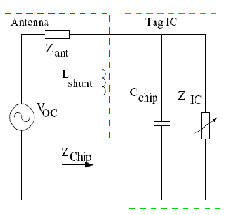
antenna across the tag’s IC. The impedance matching network between the chip and antenna is designed such that Lant term cancels at ω of choice, e.g.915MHz. This leads to a simplified antenna equivalent circuit of Rant[10]. The design of the
components assume an operating frequency of 915MHz, however, RFID systems operate within a section of the UHF
band, typically 860 − 950MHz.
Define ZIC to be composed of three subcomponents Cmod, Rmod, and RTag in parallel. RTag models the input impedance of all tag IC components other than the modulator. Cmod and Rmod are both variable components that make up part of Zmod. Thus the power delivered to RTag is the power available for use on the tag. The value of RTag is chosen to equal Rant so that during non- backscatter, the maximum amount of energy transferred from the antenna to the tag is given by:
Pma tc h =![]()
VOC
(a)
8Rant
(5)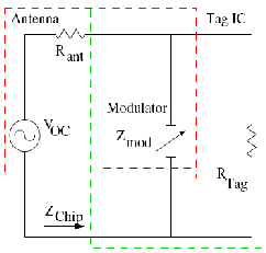
From Eqn.(5), it is clear that any power delivered to Rmod
cannot be utilized by the IC and is considered as wasted.
A variable Zmod consists of a variable capacitor (bank of varactors), chip capacitance, variable resistor (switched), and a shunt inductor in parallel. Variable components are controlled by the on-tag logic, which can be either a micro-controller or a hardwired state machine. Each set of resistive and capacitive values map to a specific Zmod value, given by:
Zmod = Rmod || jLshunt ||
1
![]()
j (Cmod Cchip )
(6)
The mean value of Cmod is chosen such that Cmean + Cchip
cancel out Lshunt at the frequency of operation, ωc, i.e.,
1
(b)
Cmean =
![]()
2
c shunt
C chip
(7)
Figure 2. Tag circuit model before the matching network: (a)
This choice of Cmean in Equation (7) tunes out Cchip and Lshunt,
resulting in Lshunt | | (Cmean + Cchip) = j∞; capacitance values greater
(less) than Cmod generate positive (negative) reactances,
respectively. In general, the combination of Lshunt and Cmod+Cchip
illustrates the model antenna inductance and chip capacitance. Whereas (b) has a matching network with the variable components of ZIC, Cchip, and Lshunt composing Zmod.
IJSER © 2013
International Journal of Scientific & Engineering Research, Volume 4, Issue 4, April-2013 424
ISSN 2229-5518
![]()
The communication between the reader and tags is achieved by backscatter modulation in which the tag switches its load impedance, which ultimately modulates the radar cross-section (RCS) of the tag. In backscatter networks, the reader transmits a high power continuous waveform. Backscatter nodes transmit their signal by reflecting back the continuous waveform using ON-OFF keying. The nodes transmit a “1” bit by changing the impedance on their antennas to reflect the reader’s signal and a “0” bit by remaining in their initial silent state.
There are four main distinctions between backscatter networks and the more familiar WiFi networks.
• There is no carrier frequency offset _fc between different
nodes’ transmissions since nodes do not generate their own RF
signal but rather reflect the reader’s signal.
• Backscatter nodes transmit and receive in a narrow bandwidth due to their power limitation. As a result, the multipath effect of wireless communication is negligible and the system can be modeled as a single tap channel (one complex number) .
• Nodes are naturally synchronized by the reader’s query and
small synchronization errors do not matter since they transmit at very low bit rates (tens to hundreds of kbps).
• The reader is a single power-full device and decoding complexity can be delegated to it while keeping the backscatter
nodes simple and power efficient.
During backscatter operation the reader transmits a constant carrier wave that illuminates the tag’s antenna with an electromagnetic (EM) field. Corresponding to the physical properties and impedance loading of the tag, a portion of the impinging EM wave is backscattered from the tag. The backscattered wave comprises of two components: a) structural mode and b) antenna mode scattering. Structural mode scattering depends on the physical properties of the antenna, and antenna mode scattering depends on the antenna’s impedance load. The physical configuration of the antenna remains independent of any impedance load placed on the antenna [13]. It has been shown by [5] that the net electric field scattered from a tag is
K a is the Volts per meter per Ampere the electric field strength radiated by the antenna per unit Ampere of antenna current.
In (9), Γi is the only term the tag can modulate with its impedance; the remaining terms are effectively constants. Furthermore, the work of [5] proves that the effect of structural scattering equates to adding a constant offset to a modulated signal. A common approach by the literature assumes![]()
![]()
E scat = Imatch K a,
![]()
thereby making E sca t ∝ Iant; Iant as the current through the antenna. For the subsequent discussion, we assume an additive
white gaussian noise (AWGN) model and perfect knowledge at the receiver of the constant offset, phase rotation, and symbol
synchronization. The net received signal at the reader y ∈ C is
the sum of three components: a) the modulated antennamode
scattering xi, b) L as the constant offset from transmit to receive leakage and structual scattering and c) WGN, i.e.,
yi = h xi + L + w (10)
where w ∼ CN(0,N0) and h is a random phase rotation.
The first term in (9) is called the structural scattering or
residual scattering component. It arises from the current induced
on the antenna conducting surface by the incident wave and is load independent. The second term is called the antenna mode component of the scattering field because it is related to the radiation property of the antenna. It is a load-dependent term and vanishes when the antenna is conjugate-matched as the reflection coefficient becomes zero.
Based on the observation from (9) that a careful choice of modulating load impedance ZL can yield a scattered –field component in any quadrant of the complex plane, a series of modelling exercises were conducted to simulate a practical backscatter QAM modulator. Modulating impedance values can be chosen by first writing each symbol of the desired I/Q constellation in the form![]()
![]()
![]()
scat = E struct - iImatch K a
(9)
S i xi jyi
where xi represents the in-phase component and
(11)
yi represents
Where
Γi =![]()
Z IC Rant
Z IC Rant
is the reflection coefficient for the i-
the quadrature component of the ith symbol. In order to produce
1impedance values realizable with passive components, all reflection coefficients are confined within a circle about the conjugate match with magnitude ≤ 1. These reflection coefficients are then scaled by a constant 0 < α ≤ 10.
th modulator state;![]()
![]()
E struct is the structural scattering term;
VOC
* .
![]()
S i
max S
(12)
Imatch =
2Rant
is the current through Rant when the
Values of α closer to 1 reflect increasing amounts of the
incident RF power back to the reader and thus result in higher
impedance of the chip and antenna are conjugate matched;
backscatter signal strength. Values of α << 1 are typical for a
passive tag to permit a majority of the incident field to be
absorbed in the energy harvesting circuit. Since α is a constant
IJSER © 2013
International Journal of Scientific & Engineering Research, Volume 4, Issue 4, April-2013 425
ISSN 2229-5518
that relates power reflection and power transmission coefficients, the optimal value will depend on the desired balance between backscattered signal power and power delivered to the energy harvesting circuit.
By rearranging the conjugate reflection coefficient * from (9), we find a set of complex impedance values for a given I/Q constellation
where λ is the wavelength, Pt is the power transmitted by the RFID reader. Gt, is the gain of the transmitting antenna (PtGt is EIRP, equivalent isotropic radiated power), Gr is the gain of the receiving tag antenna, and Pth is the minimum threshold power necessary to power up the chip. Typically Pt, Gt, Gr, and Pth are slow varying, and is dominant in frequency dependence and primarily determines the tag resonance.
![]()
Z * Z *
![]()
Z a i
(13)
L * *
i
normalized to Z * , the conjugate of the antenna impedance. The resulting modulating impedances will then fall in all four quadrants of a modified Smith chart normalized to Z0= Z a .
It is well-known from communication theory that increasing the number of constellation points improves the bit rate but also requires an increase in SNR at the receiver to preserve BER performance. The performance of the backscatter uplink (determined by constellation choice and forward error correction. Increasing the constellation order from binary signaling to QAM doubles the spectral efficiency, but causes further power loss per bit. This work investigates how the co-design of the 4-QAM constellation geometry and forward error correction (FEC) may be used to balance the normalized power loss per bit and increased spectral efficiency.
Denote the power harvested under conjugate matched conditions as Pmatc h, the average power harvested during backscatter as Pavg, and information bits per symbol (C), then introduce the metric, the normalized power loss per information bit
Ploss = (Pmatch − Pavg)/C Pmatch (13)
Backscatter, when there is an impedance mismatch between the tag and antenna, results in a power penalty to the tag. Hence for a symbol period Ts, the average energy lost per symbol due to mismatch is Ts(Pmatch − Pavg); if no backscatter occurs, the energy harvested per symbol period is TsPmatch. Normalizing the energy lost with respect to the maximum energy harvested per symbol, Equation (13) gives (Pmatch−Pavg)/Pmatc h the average fraction lost per symbol. To account for different spectral efficiency (C), use the percentage of power lost per bit or normalized power loss per bit. The FEC coding is used to improve (lower) Ploss required for QAM as compared to the uncoded case.
Read range is an important characteristic of the RFID tag. It is the maximum distance from which the tag can be detected. One limitation on the range is the maximum distance from which the tag receives just enough power to turn on and scatter back. Another limitation is the maximum distance from which the reader can detect this scattered signal. Theoretical read range rmax depends on the power reflection coefficient and can be calculated using the Friis free-space formula as
Current passive and semipassive RFID tag modulators are designed either to modulate the real part of the tag integrated circuits (IC)’s reflection coefficient, yielding ASK backscatter, or the imaginary part, yielding PSK backscatter. The most common circuit implementation of ASK for passive devices switches between a matched state, which maximizes power delivered to the passive tag’s power rectifier circuitry, and a load resistance that introduces a deliberate mismatch to produce a backscatter signal. A binary PSK modulation circuit, where the modulating transistor switches a capacitance across the antenna’s terminals to introduce a phase shift in the scattered field.
Since typical RFID readers employ homodyne receivers, the backscatter link is coherent to the reader’s transmit local oscillator. As the tag moves radially outward from a reader, the phase of the backscatter field incident on the receiver rotates at a rate of radians per half-wavelength of distance. At the 860–950- MHz frequencies typically used for UHF RFID, this leads to a rotation of every 16 cm.
Since the reader to tag distance is usually initially unknown and both ASK and PSK modulation schemes are permitted by most RFID standards, the reader must be able to demodulate tag signals arriving at any phase. For binary modulation schemes such as ASK or PSK, the reader’s baseband signal processing software typically rotates the received signal vector from its arrival angle in the I/Q plane back to the in-phase axis prior to data slicing to demodulate the tag’s binary data. Most existing RFID reader hardware is therefore not restricted to binary ASK/PSK backscatter modulation. While upgraded reader baseband signal processing software would be required to demodulate M-ary QAM data with some increase in computational complexity, QAM demodulation is supported by the existing RFID reader architecture.
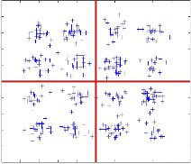
The coded QAM modulation scheme for RFID tag was designed and simulated using MATLAB 2011a software. Device- level simulation and measurements of a QAM modulator are presented for the tag operating in the frequency 850-950 MHz band.The performance of the coded QAM modulation scheme was tested by Bit Error Rate (BER) simulations for a range of SNR values. Fig.3 shows the received signal constellation generated by the backscatter modulator with random I and Q data. Digitally generated additive white Gaussian noise (AWGN) was summed with the captured time-domain signal samples. A minimum distance soft decision demodulator was used to obtain BER curves for the constellations. The resulting measured BER
curves, shown in Fig. 4, showed good agreement with those
rmax
![]()
![]()
(14)
4
predicted by MATLAB simulation.
IJSER © 2013
International Journal of Scientific & Engineering Research, Volume 4, Issue 4, April-2013 426
ISSN 2229-5518
From the BER plot, it is analysed that the probability of error for the coded QAM is reduced when compared with uncoded QAM. Fig.5 shows the received signal power after the multipath effect and it is found that the power dissipation is only115nW. In general, an M-ary QAM modulator can be clocked slower by a factor of log2M. The power dissipation in all of these sections
will thus decrease in accordance with the (1/2)CV2f model for
CMOS power dissipation. Higher order constellations can improve modulator power efficiency further.
QAM constellation plot
5
4
3
2
1
0
-1
-2
-3
-4
-5
-5 -4 -3 -2 -1 0 1 2 3 4 5
inphase
Figure 3. I/Q Baseband Constellation
BER plot
0

10
Chcode error
Unchcode error
-1
10
-2
10
-3
10
0 2 4 6 8 10 12
snr/db
Figure 4. BER for 16-QAM modulation
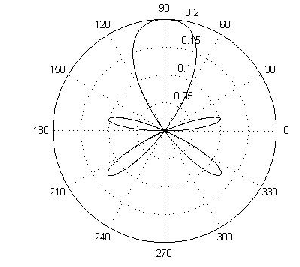
Figure 5 Received signal after change in distance antenna elemants has psi=60,F=915,N=16,d=0.5 and L=0.5
Coded 16QAM backscatter modulation was designed to improve the spectral efficiency for the UHF RFID transponder. By improving the spectral efficiency and normalizing the power loss per bit, the read range between the tag and the reader was increased. The performance of the backscatter modulation scheme was shown by the BER simulations. For the SNR value of 8dB, the bit error rate of coded QAM is only 0.002 bits per second compared to uncoded QAM. It is concluded that modulation with good error control coding provides higher spectral efficiency with a static power consumption of only
115nW. Future work will expand upon this system by implementing higher order constellations and improving signal processing for multipath robustness with increased read range.
[1] D.Yeager, Powledge.P, Prasad.R, Wetherall.D, and Smith.J, (2008), “Wirelessly-charged UHF tags for sensor data collection,” in Proc.IEEE International Conference on RFID, pp.
320–327.
[2] Sample A, Yeager.D, Powledge.P, and Smith.J, (2007), “Design of a passively powered, programmable sensing platform for UHF RFID systems,” in Proc. IEEE International Conference on RFID, pp. 149–156.
[3] R.Chakraborty, Roy.S, and Jandhyala.V, (2011), “Revisiting RFID link budgets for technology scaling: range maximization of RFID tags,” IEEE Trans. Microwave Theory and Techniques, Vol. 59, No. 2, pp. 496–503.
[4] A.Bletsas, Dimitriou.A.G, and J. Sahalos, (Jun.2010 ),“Improving
backscatter radio tag efficiency,” IEEE Trans. Microw. Theory
Tech., Vol. 58, no.6, pp. 1502–1509.
[5] Colby Boyer and Sumit Roy,(2012),“Coded QAM Backscatter Modulation for RFID”, IEEE Trans. Commun. Remote Sens., Vol.60, No.7, pp.1925- 1934.
[6] Dennis E Brown, (2007), “RFID Implementation”, Tata Mc- Graw Hill publications, New York, pp.1-327.
[7] F.Fuschini, Piersanti.C, Paolazzi.F, and Falciasecca.G, (2008), “Analytical approach to the backscattering from UHF RFID
IJSER © 2013
International Journal of Scientific & Engineering Research, Volume 4, Issue 4, April-2013 427
ISSN 2229-5518
transponder,” IEEE Antennas and Wireless Propag. Lett.,Vol. 7, pp. 33–35.
[8] S.Thomas and Reynolds.M.S, (2010), “QAM backscatter for passive UHF RFID tags,” in Proc. IEEE International Conference on RFID, pp. 210–214.
[9] M.Simon and D.Divsalar, :Some interesting observation for certain line codes with application to RFID”,IEEE Trans. Commu., Vol.54, pp.583-586, Apr.2006.
[10] G.D.Vita and Iannacone.G, (2005), “Design criteria for the RF section of UHF and microwave passive RFID transponders,” IEEE Trans. MicrowaveTheory and Techniques, Vol. 53, pp.
2978–2990.
[11] Karthaus.U and Fischer.M,(2003), “Fully integrated passive UHF RFID transponder IC with 16.7- μ W mini mum RF input power,” IEEE J.Solid-State Circuits, Vol. 38, pp. 1602–1608.
[12] P.Nikitin, Rao.K, and Martinez.R (2007), “Differential RCS of
RFID tag,” Electron. Lett., Vol. 43, no. 8, pp. 431–432.
[13] P.Nikitin, Rao.K, S. Lam, V. Pillai, R. Martinez, and H.
Heinrich, (Sep. 2005), “Power reflection coefficient analysis for complex impedances in RFID tag design,” IEEE Trans. Microw. Theory Tech., Vol. 53, no. 9, pp.2721–2725.
[14] Yao Xi, Sungwook Kwon, Hyungchul Kim, Hanjin Cho, Minsu Ki m, Sungchan Jung, Cheon-Seok Park, Jihong Kim, and Youngoo Yang, (2009), “Optimum ASK Modulation Scheme for Passive RFID Tags Under Antenna Mismatch Conditions”, IEEE Trans. Microwave Theory and Techniques, Vol. 57, No.10., pp.2337-2343.
[15] Yuan Yao, Jie Wu, Yin Shi and Fa Foster Dai, (2009), “A Fully
Integrated 900-MHz Passive RFID Transponder Front End With Novel Zero-Threshold RF–DC Rectifier”, IEEE Trans. Industrial Electronics, Vol.56, No.7., pp. 2317-2325.
IJSER © 2013