The research paper published by IJSER journal is about Improvement of Commutation Time in Matrix Converter 1
ISSN 2229-5518
Improvement of Commutation Time in Matrix
Converter
Indrajit Sarkar, Sumanta Kumar Show, Prasid Syam
Abstract— Matrix Converter is a near ideal static frequency changer which provides solution to the problem of converting ac from one frequency and one magnitude to variable frequency and variable magnitude ac, without any bulky energy storing components like capacitors or induct ors. One of the major obstacles towards commercial acceptance of this topology has been the commutation of the bidirectional switch es. An attempt has been made here to find a very fast and simple but safe current commutation technique. It has been found that with simple modification of the Input Current Filtering circuit and Diode Clamp circuit; the Stepless current commutation can be achieved giving the fastest, safe and simplest commutation technique without any voltage & current sensors and complex commutation steps. The different aspects of this realization are verified through s imulation in PSPICE and Hardware implementation. The challenges still unresolved are also mentioned.
Index Terms— Commutation Time, Current Commutation, Diode Clamp Circuit, Matrix Converter, Input Current Filter, Stepless Current Commutation, Undamped LC Filter
—————————— ——————————
OWER frequency changer is an integral part of ac drive applications. From power quality point of view, it is desir-
able to use a compact voltage source converter to provide si-
nusoidal output voltages with varying amplitude and fre- quency, while drawing sinusoidal input currents with unity power factor from the ac source. The Matrix Converter offers an almost all silicon solution for nearly ideal solid state power frequency changer [1].
The important features of Matrix Converter are - (a) Simple and compact power circuit
(b) Generation of load voltage of variable amplitude and fre- quency
(b) Sinusoidal input and output current waveforms with re- duction of higher order harmonics
(c) Control over input power factor irrespective of loads
(d) Inherent bi-directional power flow
(e) Minimum energy storage requirement
Although it can fulfil all of these ideal characteristics, there is however some practical issues in its implementation. Since there are no freewheeling paths, it is difficult to reliably commutate current from one bi-directional switch cell to other, without interrupting the load current and simultaneously not causing input short circuit. Thus commutations are usually carried out in different steps and commutation time thus de- pends on the switching time of the devices undergoing com- mutation, implying it limits the maximum switching fre-
————————————————
![]() Indrajit Sarkar is currently pursuing Masters in Electrical Engineering (Specialization - Power Electronics And Drives) at Bengal Engineering And Science University (BESU), Shibpur, India, PH-+918296327818. E- mail: jsr.indrajit@gmail.com
Indrajit Sarkar is currently pursuing Masters in Electrical Engineering (Specialization - Power Electronics And Drives) at Bengal Engineering And Science University (BESU), Shibpur, India, PH-+918296327818. E- mail: jsr.indrajit@gmail.com
![]() SumantaKumar Show is currently working at IIT Kharagpur, India as a
SumantaKumar Show is currently working at IIT Kharagpur, India as a
Project Assistant, PH-+919932582375. E-mail: sumanta.show@gmail.com
![]() Prasid Syam, Professor, Department of EE, BESU, Shibpur, India, PH-
Prasid Syam, Professor, Department of EE, BESU, Shibpur, India, PH-
+919836893676. E-mail: prasidsyam@yahoo.co.uk, ps@ee.becs.ac.in
quency.
Matrix Converter uses an array of self controlled bidirec- tional semiconductor switches and can give variable magni- tude variable frequency output voltage without having any dc link bulky energy storing elements. Input filters consisting of shunt capacitors and line inductors are necessary to eliminate high frequency unwanted current components entering into the supply utility. A high speed diode bridge clamp circuit connecting input and output is required to reduce over vol- tages across the switches during fault or when input supply goes off.
The process of turning off a conducting semiconductor switch and turning on a non-conducting semiconductor switch without interrupting the load current is known as Cur- rent Commutation [1]. As shown in figure 1 current commuta- tion is taking place from switch cell-S1 to switch cell-S2 for output phase U and from switch cell-S3 to switch cell-S4 for output phase V. It is an integral part of a Matrix Converter realization where load current needs to be transferred in any one of the three input phases depending upon the modulation logic using one of the three different bi-directional switch cells connecting an output phase to the input phases. A switch cell is generally constructed using IGBTs and diodes in various configurations for medium power applications.
There are different schemes used for current commutation [1-5]. All schemes try to follow the switching constraints and also take into account the finite switching times of semicon- ductor devices and sensor delays. Some of these rely on out- put current direction, while others rely on relative magnitudes of input voltages to activate the commutation stages.
Switching constrains are -
1) The input phases can never be shorted (short circuit may result large amount of currents through phases).
IJSER © 2012
The research paper published by IJSER journal is about Improvement of Commutation Time in Matrix Converter 2
ISSN 2229-5518
2) Assuming output current to be inductive in nature, the out put phases must not be left open (open circuit may destroy switches due to switching voltage spikes).
In Overlap Current Commutation, the incoming cell is fired before the outgoing cell is switched off. This would normally cause a line-to-line short circuit. Extra line inductance slow downs the rise of current so that safe commutation is achieved. This is not a desirable method since the inductors used are large. The switching time for each commutation is also greatly increased which may cause control problems.
In Dead-Time Commutation there is a period where
no devices are gated causing a momentary open circuit of the
load. Snubbers or clamping devices are then needed across the switch cells to provide a path for the load current. This method is undesirable since energy is lost during every com- mutation. The bidirectional nature of the switch cells further complicates the snubber design. The clamping devices and the power loss associated with them also results in increased con- verter volume.
Two different commutation strategies are:
i) Relative input voltage magnitude based current commuta- tion
ii) Output current direction detection based current commuta-
tion
Output current direction based we have Four Step, Three Step, Two Step and Single Step Current commutation strategies.
In contrast to the above mentioned current commuta- tion strategies, where we need either current and/or voltage sensing circuits (relative magnitudes as well as directions) to commutate switch cell currents, a Stepless Current commuta- tion strategy [9,12] is proposed where such circuits are not required. In case of Stepless Current commutation strategy switching signals are provided to both of the switches in a single switch cell simultaneously and this is done irrespective of the magnitude and directions of voltage and current. The respective switch will “On” in accordance with the direction and magnitude of voltage and current, which implies that the switching loss will remain same as that of single step current commutation, neglecting extra losses due to short circuit for very small duration of time (200 ns) if any. Commutation in- terval will reduce significantly and limited only by the turn- off/turn-on time of the devices. But Stepless Current commuta- tion results high input short circuit current, unless not limited by external circuits and high Ldi/dt voltage at the output (unless the inductive energy is not converted to capacitive stored energy) in case of output open circuit for inductive load. Input short circuit current can be limited by input cur-
rent filter circuit with appropriate modifications and output open circuit can be mitigated by Diode Clamp circuit, which normally exists for protection in Matrix Converter. In our
simulation study and hardware implementation we have adopted Stepless Current commutation strategy with some modifications in the Input Filter circuit to limit input short circuit current and with some modifications of the Diode Clamp circuit to limit output voltage spikes.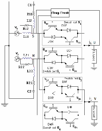
Fig. 1 Two phase to Two phase Matrix Converter with InputCurrent Filter
Circuit and Clamp Capacitor Circuit
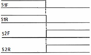
Fig. 2 Logic signal applied to the Gates of IGBT S1F, S1R, S2F and S2R
in Stepless Current Commutation
IJSER © 2012
The research paper published by IJSER journal is about Improvement of Commutation Time in Matrix Converter 3
ISSN 2229-5518
In Matrix Converter, Input Filter basically serves to mitigate near switching frequency current in the input supply lines. This filter circuit is also used for safe Stepless Current com- mutation. Preliminary idea for the filter design is taken from [5] and the analysis is extended to suit our purpose.
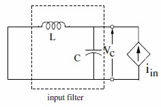
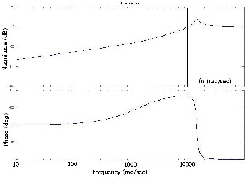
The undamped L-C passive filter is a second order filter pro- vides 12dB per octave of attenuation after the cutoff fre- quency fn. Gain = Current through filter Capacitor/ Source Current (Iin). Taking source as a current source it has no gain after fn and presents a peaking at resonant frequency fn.
Fig. 4 Gain and Phase Plots
Where fn =
2
Fig. 3 Input Current Filter
1
![]()
Hz
LC
From above MATLAB Gain and Phase plots for the LC Cur- rent filter used, the gain becomes positive and phase becomes
zero after fn.
Introduction of an extra resistance in series with filter capacitor reduces the magnitude of input short circuit current for stepless current commutation. But this will introduce fur- ther loss in the filter circuit and increase the impedance of the branch which will reduce the share of the input high fre-
In case of damped input filter -![]()
![]()
![]()
S 2 R S 1 0
L LC
Where R = Damping resistance.
Comparing it with second order equation -![]()
![]()
![]()
S 2 2 S 2
![]()
![]()
![]()

2 R , 2 1 , R C
n L n LC 2 L
Where ξ = Damping co-efficient and n = Natural frequency of oscillation.
In our study switching frequency taken as 7.8 KHz
and fn to be 1/3rd of it = 7.8/3 = 2.6 KHz. The value of filter in-
ductor and filter capacitor [10] taken as 0.78mH (as available
in the lab), 6 μF (Two capacitors in parallel 3 µF each) and the corresponding cutoff frequency fn = 2.326 KHz. Damping re- sistance used as 1 Ω and an additional resistance of 0.1 Ω is provided by the filter inductor, hence damping resistance be- comes 1.1 Ω and damping coefficient is .048.
quency current. Therefore to meet both ends the input filter is
modified as follows.
Figure 1 shows a Two phase to Two phase Matrix Converter. In our simulation study two phases are taken as 110 Volts 0° and 110 Volts 120° (50 Hz). Two outputs loads are Load1 as
48.6 Ω and 1.829 mH, Load2 59.6 Ω and 0.676 mH. Switching frequency is taken as 7.8 KHz. Inductors L12 and L22 of 70 μH are introduced in series with R-C in order to limit short circuit current as well as to reduce watt loss in R11 and R21. In this case damping co-efficient reduces a bit.
Inductor in series with R-C may block high frequency
currents through L-R-C branch resulting voltage spikes at the converter input, hence a path is provided for high frequency current components with reduced magnitude by using an- other resistor R12 and R22 in parallel with L11 and L21 of L-C filter respectively.
The Input Filter arrangement is shown in the figure 1. The L-C filter components are L11 = L21 = 0.78mH and C1 = C2 = 6 μF. These values of inductors andcapacitors are taken as only these were available in the laboratory. Damping resistance in series with filter capacitor R11 = R21 = 1 Ω and in parallel with filter inductor R12 = R22 = 120 Ω. Watt loss in R11 and R21
IJSER © 2012
The research paper published by IJSER journal is about Improvement of Commutation Time in Matrix Converter 4
ISSN 2229-5518
becomes 0.5 Watt (from 4 Watt) and watt loss in R12 and R22 is 0.2 Watt. Total watt loss in input filter is 0.7 watt.
The overvoltage protection scheme proposed is a Clamp cir- cuit [6] made up of capacitor connected to all input and all output lines through two diodes bridges as shown in figure 5. It is operative for all of the 18 IGBTs and protects the switches from the surge coming from input AC line as well as from the surge on the output side that would be otherwise produced whenever an emergency shut-down of the converter is re- quired or commutation of the switches taking place. When the output inductive currents of the motor are interrupted, the energy stored in the load is transferred to the Clamp capacitor and no critical overvoltage is caused if the capacitor is large enough.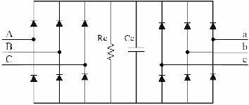
Fig. 5 Diode Clamp Circuit
Furthermore, the Clamp circuit prevents output volt- age spikes caused during current commutation by the line inductance of the power switch matrix and by the unavoidable timing inaccuracies.
Since the capacitor voltage increases at each switching
operation, some means to discharge the capacitor is required. An efficient energy removal method is to pump back the clamp energy to power system, but with Diode Bridge circuit it is not possible. Here we have used a resistor known as bleeder resistor in parallel with the Clamp capacitor to dissi- pate the clamp energy.
Converter
During fault condition the induction machine’s rotor andstator inductance stored energy will act as current source and will charge the Clamp capacitor.
Equivalent circuit of Diode Clamp circuit (per phase) in conjunction with the induction machine is shown in figure 7 [6]. IS, Ir and Im are the motor’s per phase stator current, rotor current and magnetizing current respectively. VC is the voltage
across Clamp capacitor.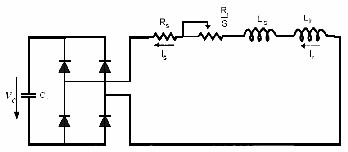
Fig. 7 Per phase equivalent circuit of Diode Clamp circuit eliminating In-
duction M/C’s shunt branch
It is assumed that the motor speed remains constant during Clamp capacitor charging.
KW, 230 Volts/Phase, 50 Hz, 3 phase, 6.5 Amps, 1400 RPM, Rotor Volts- 40 Volts/Phase, Rotor Amps – 10 Amps, Cold re- sistance of stator = 1.3 Ω /Phase, LS = Lr = 5.88 mH.![]()
Total magnetic energy stored in a three phase induc- tor carrying balanced three phase currents , , ![]() is (RMS values)-
is (RMS values)-
Q = L (ia2+ib2+ic2)/2 = 3LI2/4
Where I is the peak value of phase currents. Applying the same for a three phase induction motor and neglecting mag- netizing branch we have-
ΔQ = 3(Ls+Lr) I2/4 = 3LI2/2
Where IS = Ir = I and LS= Lr = L. Taking a safety factor of 1.5 for current, we have -
ΔQ = (3/2)3LI2
Applying energy balance equation -
½ CCVC2 = ½ CCVC02 + ΔQ
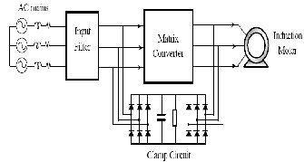
Fig. 6 Clamp circuit arrangement for three phase to three phase Matrix
½ CCVC2 = ½ CCVC02 + (3/2)3LI2
IJSER © 2012
The research paper published by IJSER journal is about Improvement of Commutation Time in Matrix Converter 5
ISSN 2229-5518
Where VC0 is the initial voltage of the capacitor Cc is the ca- pacitance value of the Clamp capacitor VC is the final voltage of Cc. Now VC0 = 3×400√2/π = 540.2 Volts and allowing Vc to be maximum of 700 Volts, L = 5.88 mH, I = 1.5*6.5 Amps Cc becomes 8.46 μF. Clamp capacitor taken as 24 μF/1000 Volts
[11].
Bleeder resistance is used to maintain a steady value of voltage across the capacitor depending on the input supply voltage. The capacitor voltage may rise above this steady value during output open circuit or input open circuit condi- tion. Bleeder resistance gives a path to discharge capacitance up to the steady value after fault condition subsides. It is i m- portant to note that diode bridges of both sides of the capaci- tor do not allow capacitor to pump back his stored energy. In our case the value of Bleeder resistor taken as 5.5 KΩ corre- sponding to Clamp Capacitor discharging time 0.13 seconds. The Clamp circuit capacitor current and the voltage across it during commutation are observed and are within limit.
The same capacitance value and bleeder resistance is suffi-
cient to keep the output voltage spikes within limitif output opencircuit condition arises during Stepless Current commu- tation. No further modification is needed.
In our study two input voltage sources are taken as 110 Volts and 110 Volts 120° at 50 Hz and two phase loads as Load1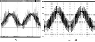
48.6 Ω and 1.829 mH, Load2 59.6 Ω and 0.676 mH. Switching Frequency 7.8 KHz. The ratio of Voltage Transducer is = 69 and that of Current Transducer is = 2.56.
Fig. 8 U phase load voltage (a) Experimental result (b) Simulated result in
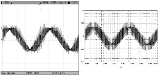
Orcad PSpice
Fig. 9 V phase load voltage (a) Experimental result (b) Simulated result in
Orcad PSpice
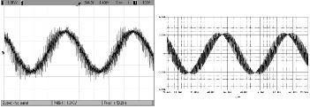
Fig. 10 U phase load current (a) Experimental result (b) Simulated result in
Orcad PSpice
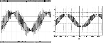
Fig. 11 V phase load current (a) Experimental result (b) Simulated result in
Orcad PSpice
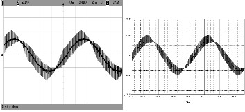
Fig. 12 R phase source voltage (a) Experimental result (b) Simulated re- sult in Orcad PSpice
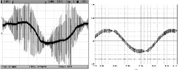
Fig. 13 R phase source current (a) Experimental result (b) Simulated result in Orcad PSpice
IJSER © 2012
The research paper published by IJSER journal is about Improvement of Commutation Time in Matrix Converter 6
ISSN 2229-5518
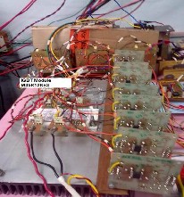
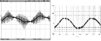
Fig. 14 S phase source current (a) Experimental result (b) Simulated result in Orcad PSpice
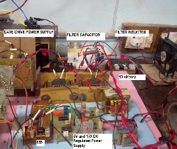
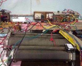
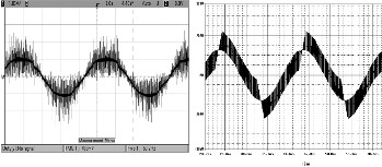 Fig. 18 IGBT Module and Driver Circuits
Fig. 15 R phase Voltage waveform at the converter input (a) Experimental
(b) Simulated in Orcad PSpice
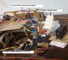
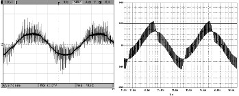 Fig. 19 Filter Circuit and Logic Circuit
Fig. 16 S phase Voltage waveform at the converter input (a) Experimental
(b) Simulated in Orcad PSpice
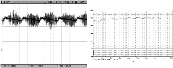
Fig. 17 Voltage across Clamp capacitor (a) Experimental (b) Simulated in
Orcad PSpice
Fig. 20 Diode Clamp Capacitor Circuit
IJSER © 2012
The research paper published by IJSER journal is about Improvement of Commutation Time in Matrix Converter 7
ISSN 2229-5518
Fig. 21 Two phase R-L Loads
[3] P.Wheeler, J. Clare, L. Empringham, M. Bland, M.Apap, “Gate Drive level Intelligence and Current Sensing for Matrix Converter current Commutation” IEEE Trans. Ind. Electron, vol. 49, pp. 382-389, Apr.
2002.
[4] L.Empringham, P. W. Wheeler, and J. C. Clare, “ Intelligent commuta- tion of matrix Converter Bidirectional switch cells using novel gate drive techniques” in Proc. IEEE PESC’98, 1998, pp. 721-726
[5] P.wheeler and D.Grant, “Optimization input filter design and low-loss
switching technique for a practical matrix converter” IEE Proceedings of
Electric Power Applications, vol. 144, no. 1, pp 53-60, Jan. 1997
[6] Peter Nielsen, Frede Blaabjerg, Senior Member, IEEE, and John K.
Pedersen, Member, IEEE “New Protection Issues of a Matrix Converter: Design Considerations for Adjust able-Speed Drives” IEEE Transactions on Industry Applications, Vol 35, No. 5, September/October 1999
[7] A.Dasgupta, S.Mukherjee, M.Sengupta, P.Syam and
A.K.Chattopadhyay “Implementation of Universal Logic System of Ge n- erating Commutating Pulses in Matrix Converters using FPGAs”, IEEE- ICIT06, Mumbai, December 2006 (Proceedings in CDROM), pp
1436-1441
[8] Ned Mohan, William Robbins and Tore Undeland, “Power Electron- ics converters, Applications and Design” Media Enhanced third edition,
Stepless Current commutation techniques are studied in depth. The reductions of input short circuit current, overshoot of voltages and commutation intervals are the major objectives of any commutation techniques.
The commutation time can be reduced to minimum possi-
ble in Stepless Current commutation technique but may cause severe input short circuit current. To reduce this short circuit current, the input filter is modified accordingly. It limits the input short circuit current to an acceptable level and presence of resistor in parallel with filter inductor eliminates any volt- age spikes to appear just after series filter inductor. The addi- tional Clamp circuit with two phase to two phase converters further improves the output voltage and current waveforms with reduction in the commutation time.
It is interesting to note that most of these passive ele-
ments are usually present in a Matrix Converter circuit for filter and protection requirements. Addition of the resistance will add to the commutation losses but its advantages will outweigh this disadvantage.
Any voltage overshoot in input and output of the con-
verter is further reduced by the presence of Diode Clamp cir- cuit.
Authors are thankful to department of Electrical Engineering, Bengal Engineering and Science University Shibpur for the encouragement and support in this work.
[1] P. Wheeler, J. Rodriguez, J. Clare, L. Empringham, A. Weinstein, “Matrix Converters: A Technology Re view,”IEEE Trans. Ind. Elec- tron., vol. 49, pp. 276-289, Apr.2002.
[2] P. Wheeler, J. Clare, L. Empringham, “Enhancement of matrix con- verter Output Waveform Quality Using Minimized Commutation Times” IEEE Trans. Ind. Electron, vol. 51, pp. 240-244, Feb. 2004.
WILEY INDIA EDITION, 2007
[9] Sumanta Kumar Show, Indrajit Sarkar, Prasid Syam, ”Exploring the possibility of Single Step Current Commutation in a Matrix Converter” NPEC-2011, BESU, Shibpur, December 2011
[10] Indrajit Sarkar, Sumanta Kumar Show, Prasid Syam, ”Role of Input Current Filter to Facilitate Single Step Commutation in Matrix Con- verter” NPEC-2011, BESU, Shibpur, December 2011
[11] Indrajit Sarkar, Sumanta Kumar Show, Prasid Syam, ”Role of Diode Clamp Circuit to Facilitate Single Step Commutation in Matrix Con- verter” NPEC-2011, BESU, Shibpur, December 2011
[12] Sumanta Kumar Show, “Single Step current commutation technique in
a Matrix Converter” ME Thesis, Dept. of EE BESU Shibpur, 2011
IJSER © 2012