International Journal of Scientific & Engineering Research, Volume 4, Issue 11, November-2013 74
ISSN 2229-5518
Implementation of Interface between AXI Protocol and DDR3 Memory for SOC
Y.Nageswara Reddy, A.Suman Kumar Reddy
Abstract— This project deals with implementation of interface for efficient SOC. It accepts the Read / write commands from AXI and convert into DDR3 access.AXI protocol is an open standard on chip interconnect specification for the connection & management of functional blocks in SOC. In this project, an interface between a master (processor/user) & slave (DDR3 memory) was designed. This interface will transfer the data from master to slave & vice versa. This interface implemented is called as DDR3 Controller, W hich is specially targated for the DDR3 memory Apart from the designing DDR3 controller, The communication is achieved between the master & the slave using various resd / write commands of AXI protocol .Certain novel features of AXI protocol like variable length burst (from 1 to 16 data transfer per burst) & fixed wrapping burst are included in the design to achieve the data transfer.Our design has been implemented with respect to latency reduction and improvement in various perfor- mance parameters and the design is simulated Modelsim Synthesized on Xilinix successfully.
Keywords— DDR3 memory, AXI interfaces, AXI access manager, DDR3 memories, AXI protocol operation.
—————————— ——————————
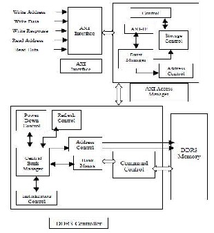
T he AXI compliant DDR3 Controller permits access of DDR3 memory through AXI Bus interface [1-4].The DDR3 controller works as an important bridge between AXI host and DDR3 memory.It takes care of DDR3 intialization and var- ious timing requirements of DDR3 memory.The DDR3 controller performs multiple schemes to increase the the effective memory throughput [3].These sceame include and reordering the Read/Write commands. For attaining the maximum throughput from the memory, it operates all the memory banks in parallel and minimizes the effect of precharge/refresh and other DDR3 internal op- erations [2].Interface between AXI protocol and DDR3 memory for SOC Architecture The architec- ture of the design is shown in the fig.1. T he design consists of following blocks-
• AXI interface
• AXI access Manager
• DDR3 Controller Fig.1 Interface between AXI protocol and
A. AXI Interface:
————————————————
• Y.N ageswar a Reddy, PG Scholar , D epartm e nt of Ele ctronics and
Com m unicatio n Eng ine er ing , PBR V isvo daya Ins titute o f Te ch no log y
& Scie nces , Kava li, A ndhr a Prade sh , Ind ia ;
nag es war ar eddy.y@g ma il . co m
• A.Suman K umar Re ddy, A sso cia te Profes sor , D epartm e nt o f Ele c- tro nics a nd Co mm unica tio n Eng ine er ing ,PBR Visvoda ya Institute o f Tech nology & Scie nces ,Kava li,A ndhr a Pra-
desh ,India;s uma n.v its@g ma il.com
IJSER © 2013
AXI-Interface block interacts with HOST processor and AXI access manager. It is responsible for accepting and interpreting the AXI commands issued by the processor and responding to Read / Write requests in AXI protocol as requested by pro- cessor. It also maintains an arbiter block which is responsible for arbitrating between Read/Write commands.Arbitaration is required between com- mands because of parlell/independent of Read /
http://www.ijser.org
International Journal of Scientific & Engineering Research, Volume 4, Issue 11, November-2013 75
ISSN 2229-5518
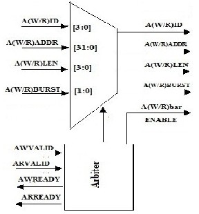
Write command received at AXI interface. It main- tains asynchronous FIFO’s to store the command and the data. The Read command gets stored in (Read Command Block), Write command gets stored in (Write Command block), Read data gets stored in (Read Data block), and Write data gets stored in(write data block).The stored commands are supplied to the AXI access manager whenever AXI access manager is free.Now since the storage can have both read and write commands in the re- spective blocks hence it maintence an arbiter which arbiterates between Read/Write command and whenever burst manager is free one of the present command is supplied to the Burst Manager
.
B. AXI Access Manager:
The main function of the AXI-Access Man- ager is to convert the AXI commands into memory access commands for maximum utilization of the DDR3 Band Width. T he DDR3 memory takes com- mand only in burst 4 or 8 mode here as the AXI command could be a smaller or longer burst. The AXI access manager combines the command when- ever possible to improve the performance and pa- sess the command to the DDR3 controller.To insure maximum throughput it prefetches the command from AXI interface converts into memory transac- tions and maintains locally.The stored commands are supplied to the DDR3 controller whenever DDR3 controller is not bustin the very next clock. The AXI-IF block interacts with the AXI interface block and receives commands. The received com- mands are stored in the Storage control block.The Burst Manager converts the AXI commans into DDR3 burst.The address control block is responsi-
ble for generation of address The overall operation of various blocks in the AXI access manager is con- trolled by the Control Logic. The fig.3 shows the AXI Access Manager Block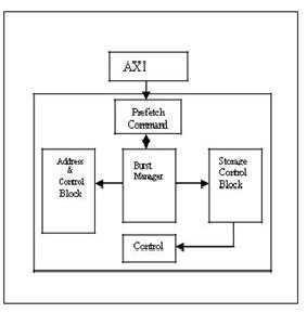
C. DDR3 Controller:
The main function of DDR3 controller is to interact with the DDR3 memory. This is the heart of the AXI compliant DDR3 controller and responsible for understanding the DDR3 protocol and com- municating with the DDR3 memory [4]. DDR3 Con- troller also issues Refresh, Power down, Self refresh command along with the read or write command as per the user configuration [1]. The internal blocks of DDR3 controller are shown in the fig.4-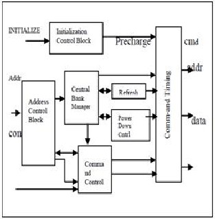
IJSER © 2013 http://www.ijser.org
International Journal of Scientific & Engineering Research, Volume 4, Issue 11, November-2013 76
ISSN 2229-5518
The Power down Control Block takes care of generating the power down command to the DDR3 memory whenever the host commands it to go to Power saving mode. The refresh control block takes cares the refreshing of DDR3 memory as per the user supplied configuration.The initialization control block take care of initializing DDR3 memory after reset. To control the timings of indi- vidual DDR3 banks it contains Bank manager which track the timing requirements for the indi- vidual DDR3 banks. The address control block is responsible for generating the address to the DDR3 memory. T he Command control block interacts with the DDR3 memory and based on the Bank manager inputs drives the DDR3 bus.It also re- sponsible for receiving the data during Read opera- tion.The central bank coordinates between the indi- vidual Bank Managers and maintains the overall timing requirements of DDR3 meory.
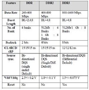
DDR3 offers a substantial performance im- prove over previous DDR2 & DDR memory systems. New DDR3 features, all transparently implemented in the memory controller, improve the signal integ- rity charecteristics of DDR3 design so that the high- er performance is achieved without an undue bur- den for the system designer. If proper consideration is given to any new DDR2 memory design, it can be a relatively easy upgrade to support DDR3 in the next generation design.
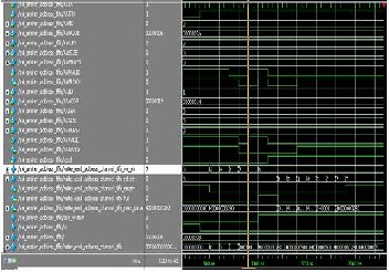
The first signal represents the clock signal of the desifed frequency and time period. On the rising edge of the second clock pulse a request is sent by the client port. It lasts for two clock pulses and then falls down. A differential clock pulse of the client’s request with attributes lasts from the rising edge of client request to the falling edge of the same. This gives all the information of the attributes. An acknowledge signalis then sent by the controller so that the user can understand therequest has been accepted by the controller. Then the differential sig- nal consisting of the write data is sent to the client port. The write data valid signal defines the data that has to be written and that it is a valid data.The Write acknowledge signal makes it clear that the da- ta has been received with bits D2,D3 being don’t care condition.
IJSER © 2013 http://www.ijser.org
International Journal of Scientific & Engineering Research, Volume 4, Issue 11, November-2013 77
ISSN 2229-5518
Verification is important part of complete designprocess.It takes almost 60% of the design process flow so to minimize time to market in com- plete design we do verification process I parallel with the design process. The verification of AXI compliant DDR3 controller is accomplished by sending the AXI transaction through the AXI Bus Functional Model. The response from the AXI com- pliant DDR3 controller is received by the AXI Bus Functional Model and is passed to the Checker. The checker also picks the expected response from the Local memory and compares it based on the com- parison the environment prints passed and failed messages and the associated data mismatch if any the verification process for implementation of inter- face between AXI protocol and DDR3 Memory for
SOC is shown in Fig 6-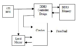
The AXI Bus Functional Model consists of generator, driver monitor and score board.T he generator generates the AXI transactions Driver is used to drive the DUT (Device under Test) here DUT is AXI interface. T he AXI transaction is also passed to the local memory which prepares the expected response which is passed to the checker whenever the checker asks for it. Upon receiving the response from the DDR3 memory checker commands the local memory to give back to the stored expected response and comares with output response with expected response.
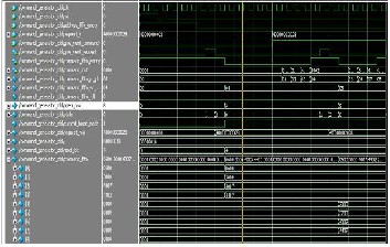
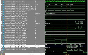
The bilow figures are snapshots of the Interface between AXI and DDR3 memory for SOC. And we can observe the individual block outputs and overall top level module put.Various operation modes. The design has been coded in “Verilog HDL” language. The functional simulation tool used in 10.1c from Modelsim.
IJSER © 2013 http://www.ijser.org
International Journal of Scientific & Engineering Research, Volume 4, Issue 11, November-2013 78
ISSN 2229-5518
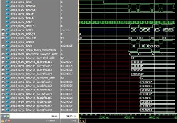
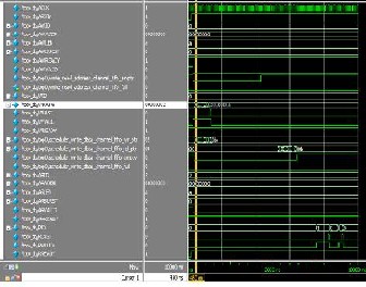
The design has been verifird by the exhaustive functional verification.User transactions are trans- ferred repeatedly, without any delayed between and its maximum operation frequency is 54.776MHz .The AXI interface is implemented with one master and one slave. T his design supports AXI protocol (32 or
64 bit) data width, remapping, run time configurable
timing parameters & memory setting, delayed
writes, multiple outstanding transactions and also supports the automatic generation refresh sequenc- es.The performance of design was examined by gen- erating different types of AXI commands and noth- ing down the time taken by the the DDR3 controller in finishing them.
Future improvement in AXI interface block is to
add more features like in burst, address remains all the same in every transfer in the burst. This burst type is for every repeated accesses to the same loca- tion such as when loading or emptying a peripheral FIFO and wrapping burst is similar to an increment- ing burst, in that the address for each transfer in the burst is an increment of the previous transfer ad- dress. However in wrapping burst the address wraps around to a lower address when a wrap boundary is reached. The write response signal other then OKEY are EXOKAY SLVERR and DECERR. Fu- ture Improvement in DDR3 Controller is to add Re- order block in between AXI Access Manager and DDR3 controller block.T he reorder block will en- hance the performance of complete DDR3 controller because it sends same row address command then sends other row address command. When we switch the transaction from Row address X to other Row address Y first we have to close Bank corresponding to that Row address X means precharge that Bank and it take tRP time to precharge the particular bank. So to achieve high performance we have to or- der the same row address command with coming da- ta from AXI Interface block. But at this time we are not implementing this block because this is applica- ble when we are firing random row address com- mand means that depend on open the customer re- quirements because this order block increase cost and size of the chip.
[1] Churoo (Chul-Woo) Park, HoeJu Chung, Yun-SangLee, Jun-Ho Shin, Jin- Hyung Cho, Seunghoon Lee, Ki-Whan Song, Kyu-Hyoun Kim,Jung-Bae Lee,Changhyun Kim, Senior Member, IEEE, and Soo-InCho.” A 512-Mb DDR3 SDRAM Prototype and Self-Calibration Techniques” Proc
[2] K. Kim et al, “A 1.4 Gb/s DLL using 2nd order chargepumpscheme with low phase/duty error for high-speedDRAM application,” in IEEE Int. Solid-state CircuitsConf. (ISSCC) Dig. Tech. Papers, 2004, pp. 212-523
[3] S.Lee et al, “ A. 1.6 Gbs/pin double data rate SDRAMwith wavepiplined CAS latency control,” in IEEE Int.Solid-State Circuits conf. (ISSCC) Dig. Tech. Papers, 2004, pp.210-213.
[4] H . S ong et al , “ A 1 .2 G bs / pi n dou bl e da t a ra t e S D R A M w i t h on di e -te r m in a tio n , ” in I EEE I n t. S o lid -S ta te C ir cu its C o n f. ( I S S C C) D i g. T e c h. P a pe r s , 20 03 , pp. 314 -496 .391 5
IJSER © 2013 http://www.ijser.org