International Journal of Scientific & Engineering Research, Volume 3, Issue 1, January-2012 1
ISSN 2229-5518
Implementation of Embedded Multiprocessor
Architecture Using FPGA
Mr.Sumedh.S.Jadhav, Prof.C.N.Bhoyar
Abstract— Embedded multiprocessor design presents challenges and opportunities that stem from task coarse granularity and the large num ber of inputs and outputs for each task. We have therefore designed a new architecture called embedded concurrent computing (ECC), which is implementing on FPGA chip using VHDL. The design methodology is expected to allow scalable embedded multiprocessors for system expansion. In recent decades, two forces have driven the increase of the processor performance: Advances in very large-scale integration (VLSI) technology and Micro architectural enhancements. Therefore, we aim to design the full architecture of an embedded processor for realistic to perform arithmetic, logical, shifting and branching operations. We will be synthesize and evaluated the embedded system based on Xilinx environment. Processor performance is going t o be improving through clock speed increases and the clock speed increases and the exploitation of instruction- level parallelism. We will be designing embedded multiprocessor based on Xilinx environment. These data have been gathered by synthesis. Implementation was achieved by the provision of low complexities in terms of FPGA resource usage and frequency. In addition, the design methodology allows scalable embedded multiprocessors for system expansion.
Index Terms— Embedded System design, FPGA ,Memory Architecture, Real time Processor, Scheduler, VHDL Environment, Xilinx Environment.
—————————— ——————————
1 INTRODUCTION
n recent decades, two forces have driven the increase
of the processor performance: Firstly, advances in very large- scale integration (VLSI) technology and secondly
micro architectural enhancements [1].
Processor Performance has been improve through clock speed Increases and the exploitation of instruction-level Parallelism. While transistor counts continue to increase, recent attempts to achieve even more significant increase in single-core performance have brought diminishing returns [2, 3]. In response, architects are building chips With multiple energy-efficient processing cores instead of investing the whole transistor count into a single, complex, and power-inefficient core [3, 4]. Modern embedded systems are design as systems-on a-chip (SoC) that incorporate single chip multiple Programmable cores ranging from single chip multiple programmable cores ranging from processors to custom designed accelerators. This paradigm allows the reuse of pre- designed cores, simplifying the design of billion transistor chips, and amortizing costs.
In the past few years, parallel-programmable SoC (PPSoC)have Successful PPSoC are high-performance embedded multiprocessors such as the STI Cell [3] .They are dubbed single-chip heterogeneous multiprocessors (SCHMs) because they have a

Sumedh.S.Jadhav masters degree program in VLSI engineering in R.ST.M.N.University, India, PH-09860139771 E-mail: sumedh_jadhav@rediffmail.com
Prof.C.N.Bhoyar masters degree program in VLSI engineering in
S.G.University, India, PH-09923696276.
E-mail: cnbhoyar@gmail.com
dedicated processor that coordinates the rest of the processing units. A multiprocessor
design with SoC like integration of less-efficient, general-purpose processor cores with more efficient special-purpose helper engines is project to be the next step in computer evolution [5].
First, we aim to design the full architecture of an embedded processor for realistic throughput. We used FPGA technology not only for architectural exploration
but also as our target deployment platform because we
believe that this approach is best for validating the
feasibility of an efficient hardware implementation.
This architecture of the embedded processor resembles a
superscalar pipeline, including the fetch, decode, rename,
and dispatch units as parts of the in-order front-end. The out of-order execution core contains the task queue, dynamic scheduler; execute unit, and physical register file. The in order back-end is comprised of only the retire unit. The embedded architecture will be implement using the help of RTL descriptions in System VHDL.
We will integrate the embedded processor with a shared memory system, synthesized this system on an FPGA environment, and performed several experiments using realistic benchmarks. the methodology to design and implement a microprocessor or multiprocessors is presented. To illustrate it with high detail and in a useful way, how to design the most complex practical session is shown. In most cases, computer architecture has been taught with software simulators [1], [2]. These simulators are useful to show: internal values in registers, memory
IJSER © 2012 http://www.ijser.org
International Journal of Scientific & Engineering Research, Volume 3, Issue 1, January-2012 2
ISSN 2229-5518
accesses, cache fails, etc. However, the structure of the microprocessor is not visible.
In this work, a methodology for easy design and real Implementation of microprocessors is proposed, in order to provide students with a user-friendly tool. Simple designs of microprocessors are exposed to the students at the beginning, rising the complexity gradually toward a final design with two processors integrated in an FPGA; each of which has an independent memory system, and are intercommunicated with a unidirectional serial channel.
2 MULTIPROCESSOR
Multiprocessor system consists of two or more Connect processors that are capable of communicating. This can be done on a single chip where the processors are connected typically by either a bus. Alternatively, the multiprocessor system can be in more than one chip, typically connected by some type of bus, and each chip can then be a multiprocessor system. A third option is a multiprocessor system working with more than one computer connected by a network, in which each
Computer can contain more than one chip, and each chip can contain more than one processor.
A parallel system is presented with more than one
task, known as threads. It is important to spread the workload over the entire processor, keeping the difference in idle time as low as possible. To do this, it is important to coordinate the work and workload between the processors. Here, it is especially crucial to consider whether or not some processors are special-purpose IP cores. To keep a system with N processors effective, it has to work with N or more threads so that each processor constantly has something to do. Furthermore, it is necessary for the processors to be able to communicate with each other, usually via a shared memory, where values that other processors can use are stored. This introduces the new problem of thread safety. When thread safety is violated, two processors (working threads) access the same value at the same time. Some methods for restricting access to shared resources are necessary. These methods are known as thread safety or synchronization. Moreover, it is necessary for each processor to have some private memory, where the processor does not have to think about thread safety to speed up the processor. As an example, each processor needs to have a private stack. The benefits of having a multiprocessor are as follows:
1. Faster calculations are made possible.
2. A more responsive system is created.
3. Different processors can be utilized for different
Tasks. In the future, we expect thread and process
parallelism to become widespread for two reasons: the nature of the Applications and the nature of the operating system. Researchers have therefore proposed two
alternatives Micro architectures that exploit multiple threads of Control: simultaneous multithreading (SMT) and chip multiprocessors (CMP). Chip multiprocessors (CMPs) use relatively simple.
Single-thread processor cores that exploit only moderate
amounts of parallelism within any one thread, while executing multiple threads in parallel across multiple processor cores. Wide-issue superscalar processors exploit instruction level parallelism (ILP) by executing multiple instructions from a single program in a single cycle. Multiprocessors (MP) exploit thread-level parallelism (TLP) by executing different threads in parallel on Different
processors.
3 EMBEDDED SYSTEMS AND SYSTEM DESIGN
3.1 Characteristics of Embedded Systems
The earliest embedded systems were banking and transaction processing systems running on mainframes and arrays of disks. The design of such a system entails hardware- software co-design: given the expected number and type of transactions to be made in a day, a hardware configuration must be chosen that will support the expected traffic and a software design must be created to efficiently make use of that hardware. When microprocessors are used to create specialized, low-cost products, engineering costs must be reduced to a level commensurate with the cost of the underlying hardware.
Because multiprocessors can be used in such a wide range of products, embedded systems may need to meet widely divergent criteria. Examples of embedded systems include:
simple appliances, such as microwave ovens,
where the multiprocessor provides a friendly interface and advanced features;
an appliance for a computationally intensive
task, such as laser printing;
Embedded system design can be divided into four major tasks:
partitioning the function to be implemented into smaller, interacting pieces;
allocating those partitions to multiprocessors or
other hardware units, where the function may be impel- meted directly in hardware or in software running on a multiprocessor.
scheduling the times at which functions are executed, which is important when several functional partitions share one hardware unit;
mapping a generic functional description into an
implementation on a particular set of components, either as software suitable for a given
IJSER © 2012 http://www.ijser.org
International Journal of Scientific & Engineering Research, Volume 3, Issue 1, January-2012 3
ISSN 2229-5518
microprocessor or logic which can be implemented from the given hardware libraries.
4 SOFTWARE TOOL
The Xilinx Platform Studio (XPS) is used to design Micro Blaze processors. XPS is a graphical IDE for developing and debugging hardware and software. XPS simplifies the procedure to the users, allowing them to select, interconnect, and configure components of the final system. Dealing with this activity, the student learns to add
• To assign drivers to peripherals.
• To assign interruption drivers.
• To establish OS and libraries’ parameters.
• To assign Input/output port.
• To assign timers.
• To establish components parameters.
.
MEMORY
processors and peripherals, to connect them through buses,
to determine the processor memory extension and
allocation, to define and connect internal and external ports, and to customize the configuration parameters of the components. Once the hardware platform is built, the students learn many concepts
about the software layer, such as: assigning drivers to
Peripherals, including libraries, selecting the operative system (OS), defining processor and drivers parameters, assigning interruption drivers, establishing OS and libraries
CLK
RESET
SCHEDULLER
TIMING UNIT ENABLE
ALU
OUTPUT
parameters.
An embedded system performed with XPS can be
Summarized as a conjunction of a Hardware Platform
(HWP) and a Software Platform (SWP), each defined separately.
4.1 Hardware Platform
The HWP is described in the Microprocessor Hardware Specification (MHS) file; it contains the description of the system architecture, the memory map and the configuration parameters. HWP can be defined as one or more processors connected to one or more peripherals through one or more buses. The definition of the activity follows this sequence:
• To add processors and peripherals.
• To connect them through buses.
• To determine the processor memory allocation.
• To define and connect internal and external ports.
• To customize the configuration parameters of the
Components.
4.2 THE SOFTWARE PLATFORM
The SWP is described in the Microprocessor Software Specification (MSS) file; it contains the description of drivers, component libraries, configuration parameters, standard input/output devices, interruption routines and other software features. The sequence of activities needed to define the SWP
is the following:
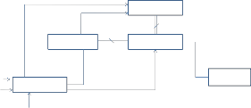
Figure 1. Block diagram of Multiprocessor
4.3 System Memory
A system that complies with the MP specification uses the standard AT memory architecture. All
memory is allocated for system memory with the exception of addresses 0A_0000h through
0F_FFFFh and 0FFFE_0000h through 0FFFF_FFFFh, which
are reserved for I/O devices and the
BIOS.
Compared to a uniprocessor system, a symmetric
multiprocessor system imposes a high demand
for memory bus bandwidth. The demand is proportional to
the number of processors on the
memory bus. To reduce memory bus bandwidth limitations, an implementation of this
specification should use a secondary cache that has high- performance features, such as a write-back
update policy and a snooping cache-consistency protocol. A
secondary cache can push the
scalability limit upward by reducing bus traffic and
increasing bus bandwidth.
In this form of multiprocessing, each background process renders its own frame and runs on a separate processor core (CPU). The number of processes used to render multiple frames simultaneously is never more than the number of processors. The number of background processes that can run on your computer also depends on the total amount of installed system RAM and the amount of RAM that is assigned to the After Effects application.
IJSER © 2012 http://www.ijser.org
International Journal of Scientific & Engineering Research, Volume 3, Issue 1, January-2012 4
ISSN 2229-5518
4.4 Scheduler
• To assign drivers to peripherals.
• To assign interruption drivers.
• To establish OS and libraries’ parameters.
• To assign drivers to performs specific tasks.
• To support multiprogramming
• Large numbers of independent processes
• Simplified administration
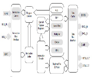
Figure 2. Proposed architecture of multiprocessor architecture.
5 THE MICROBLAZE PROCESSOR
Micro Blaze is a 32-bit specific purpose processor Developed by Xilinx in VHDL. It can be parameterized using XPS to obtain an à-la-carte processor. It is a RISC processor, structured as Harvard architecture with separated data and instruction interfaces. Micro Blaze components are divided into two main groups depending on their configurability as shown in Fig.1. Some fixed feature components are:
• 32 general purpose registers sized 32-bit each.
• Instructions with 32 bits word-sized, with 3 operands
and 2 addressing modes.
• 32 bits address bus.
• 3-stage Pipeline.
Some of the most important configurable options are:
• An interface with OPB (On-chip Peripheral Bus) data
bus.
• An interface with OPB instruction bus.
• An interface with LMB (Local Memory Bus) data bus.
• An interface with LMB instruction bus.
• Instruction cache.
• To include EDK libraries.
• To select the operative system (OS).
• To define processor and drivers’ parameters.
• Data cache.
• 8 Fast Simplex Link (FSL bus) Interfaces.
• Cache Link bus support.
• Hardware exception support.
• Floating Point Unit (FPU).
The suggested core embedded processor contains
a dual-issue, superscalar, pipelined processing unit, Along with the other functional elements required to Implement embedded SoC solutions. This other Functions include memory management and timers.
6 PRACTICAL DESIGNS
Practical sessions introduce gradual learning, allowing the fast design based on previous sessions. Essential problems in hardware programming will be raised:
• HyperTerminal serial communication.
• Using IO ports.
• Memory controller.
• Interruption routines and priority.
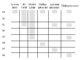
Figure 3. Sessions and contents.
• Message passing in multiprocessors communication. The practical content of the subject is composed of 8
Projects. In the first session, user makes a basic system which will be used in following sessions as the base core system. Second and third sessions are used to introduce the input/output flow and the communication with external peripheral through the On-chip Peripheral Bus, for general purpose. SRAM external memory is added to the system at fourth session. Next session is dedicated to the External Memory Controller and how to split the bus. Micro Blaze interruptions are added in the sixth session, and external interruptions using the interruption controller are included in the seventh session. Finally, students build a biprocessor, using the Fast Simple Link channel at session eight. In fig.
2.
Relation between practices is shown. For instance, 5th session is based on all previous sessions, 7th session is based on 3rd and 1st Session.
IJSER © 2012 http://www.ijser.org
International Journal of Scientific & Engineering Research, Volume 3, Issue 1, January-2012 5
ISSN 2229-5518
7 BIPROCESSOR SYSTEM DESIGN
The last and most complex practical session is the design and implementation of a biprocessor. A computational system composed of two Micro Blazes will be designed. Both Micro Blazes will be interconnected using message-passing protocol. Each Micro Blaze has its own non-shared memory for Instructions and data. In the Fig. 3 a diagram with the structure of the design is shown. In it, the buses and components used have been detailed. It also includes how they are interconnected At first, following the logical sequence exposed previously, a HWP will be created. This HWP will include the configuration of the components and buses, their interconnection, the memory map, ports and other parameters. In the following subsection, the steps needed to configure the system will be described. The parameters shown in this section depends on the FPGA chip, in this case the Spartan 3 board [11].
7.1 Hardware Platform Specifications
This stage is described in the MHS file. Following, the Components specified in the structure of the system are Enumerated:
• Two Micro Blaze processors.
• Two on-chip RAM memory blocks (BRAM), one for
Each processor.
• One UART.
• One OPB bus, to connect the UART with the slave
Processor.
• Two LMB buses to communicate each processor with Their respective data memory controller; and another Two LMB buses to interconnect the processors with Their instruction memory controller.
• One FSL channel to intercommunicate each processor
With the other.
After that, the interconnection of buses and components is defined. The connection of the memory ports are also set at this point. The student has to specify in the connection matrix which components are linked to which buses and with which kind of connection.
In the exposed case, four LMB buses are needed to access local memory, two for each Micro Blaze, because each processor has its own memory subsystem.
Also, one FSL channel which connects both processors. Each BRAM has been designed with 4 different ports. Each Micro Blaze reaches its memory block through two different interfaces (instructions and data). After that, it is necessary to map the components inside the
Configuration memory of the processors. XPS provides a functionality which is able to compute automatically a valid configuration memory map for a monoprocessor system structure. However, as the system proposed is a biprocessor one, this functionality cannot Each Micro Blaze looks for the first instruction in its Program at memory address 0x0. be used. The next step is to define the internal and external ports.
mandatory: clock, reset, UART in and UART out. With
these ports, the student sends commands and Most of the internal ones are configured by XPS with default settings. It is also necessary to define and to connect some of the internal ports to make the system works: those ports related to the reset and clock signals must be forwarded to all of the subsystems and components. Four external ports are synchronization Information to the system. Finally, the components are Configured. The parameters for each component and their meaning are described thoroughly in the documentation included in the XPS platform.
Particularly, Micro Blaze includes a parameter which
selects the amount of FSL interfaces used. Thus, both processors have to set this configuration value to one to allow the communication between them. The configuration of this parameter is done by changing C_FSL_LINKS. This parameter has to be set to a numerical value, representing the amount of FSL interfaces to be included in the core.
Another interesting configuration to be mentioned is
the UART operational configuration. The student has to determine the operational frequency, the application of the parity bit checking, working bauds, etc. A valid set of parameters for the UART and Micro Blaze are the following:
7.2 UART parameters.
a) C_CLK_FREQ = 50_000_000. Set the frequency of
the OPB bus, connected to the UART. It has to coincide
with the operational system speed.
b) C_BAUDRATE = 19200. Set the bauds for the
UART. The terminal used to receive characters has to be configured at the same baud rate.
c) C\_USE\_PARITY = 0. Set whether the UART
should work with parity bit or not.
SOFTWARE AND HARDWARE REQUIREMENT
For Software simulation I will prefer MODELSIM and for synthesis I will be prefer XILINX. Hardware requirement is SPARTAN-3.
RESULT V ERIFICATION AND ANALYSIS
Observe the required result like arithmetic, logical, branching and shifting.
IJSER © 2012 http://www.ijser.org
International Journal of Scientific & Engineering Research, Volume 3, Issue 1, January-2012 6
ISSN 2229-5518
ACKNOWLEDGEMENTS
Authors wish to remark the great task carried out by the Xilinx and Modelsim user guide; and the Sun Microsystems Opens ARC University Program, which have donated software and materials which have been very useful to partially finance this work. Author also wish to thanks Prof.C.N.Bhoyar for his contribution in the design process.
REFERENCES
[1] John L. Hennessy and David A. Patterson. Computer architecture: a quantitative approach. Morgan Kaufmann Publishers Inc., San Francisco, CA, USA, fourth edition 2007.
[2] Doug Burger and James R. Goodman. Billion-Transistor
Architectures: There and Back Again. IEEE Computer,
37(3):22–28, 2004.
[3] David Geer. Industry Trends: Chip Makers Turn to
Multicore Processors. Computer, 38(5):11–13, May,2005. [4] AMD Corporation. Multi-core processors: the next
revolution in computing White paper, 2005.
[5] B. Ackland, A. Anesko, D. Brinthaupt, S.J. Daubert, A.
Kalavade, J. Knobloch, E. Micca, M. Moturi, C.J. Nicol, J.H. O’Neill, J. Othmer, E. Sackinger, K.J. Singh, J. Sweet, C.J. Terman, and J. Williams. A Single-chip, 1.6-billion, 16-b MAC/s Multiprocessor IEEE Journal of, 35(3):412–424, Mar
2000.
[6] Asawaree Kalavade, Joe Othmer, Bryan Ackland, and K. J.
Singh. Software environment for a multiprocessor DSP. In DAC ’99: Proceedings of the 36th ACM/IEEE conference on Design automation, pages 827–830, New York, NY, USA,
1999. ACM..
[7] V. Sklyarov, and I. Skliarova. ―Teaching Reconfigurable
Systems: Methods, Tools, Tutorials, and Projects,‖ IEEE Trans. on Education, vol. 48, no. 2, 290–300, 2005.
[8] OpenSPARC http://www.opensparc.net/edu/university- program.html. Last accessed on 8th November 2009.
[9] ―Platform Studio User Guide,‖ Application notes, Xilinx,
2005.
[10] ―Microblaze Processor Reference Guide,‖ Application
notes, Xilinx, 2005.
[11] ―Embedded System Tools Reference Manual,‖
Application notes, Xilinx, 2008.
[12] ―OS and Libraries Document Collection,‖ Xilinx,
Application notes, September 2007.
[13] Spartan-3 Board. http://www.digilentinc.com/ . Last
accessed on 30th October 2009.
IJSER © 2012 http://www.ijser.org