International Journal of Scientific & Engineering Research, Volume 5, Issue 4, April-2014 1099
ISSN 2229-5518
Grid Connected Solar Microinverter Based On
Single Stage Boost Conversion
P.Jeyankondan, V.Hemamageswari, Dr. M .Santhi
Abstract— This topology represents the grid connected solar microinverter based on single stage boost conversion. This circuit can extract maximum solar power from solar panel .The output voltage of the circuit is stabilized by the use of closed loop control. Transformer gives isolation between converter circuit and inverter circuit. And also this topology reduced the number of switches needed
Index Terms— Grid connected solar microinverter.Isolated boost converter, Inverse buck converter, Maximum solar power, PV panel, Single stage boost conversion, Voltage doubler circuit.
—————————— ——————————
HE increasing number of renewable energy sources and distributed generators requires new strategies for the op- eration and management of the electricity grid in order to maintain or even to improve the power-supply reliability and quality. In addition, liberalization of the grids leads to new management structures, in which trading of energy and power is becoming increasingly important. The power-electronic technology plays an important role in distributed generation and in integration of renewable energy sources into the elec- trical grid, and it is widely used and rapidly expanding as these applications become more integrated with the grid-
based systems.
During the last few years, power electronics has un-
dergone a fast evolution, which is mainly due to two factors.
The first one is the development of fast semiconductor switch-
es that are capable of switching quickly and handling high
powers. The second factor is the introduction of real-time
computer controllers that can implement advanced and com-
plex control algorithms. These factors together have led to the
development of cost-effective and grid-friendly converters.
While fossil fuel exhaustion and greenhouse effects are widely
concerned around the world, one of the most important issues
toward these problems is to find alternative energy for long- term solutions. Green energy offering the promise of clean and abundant energy gathered from self renewing sources such as solar energy, geothermal energy, and wind source is broadly
developed. Solar cells are unique in that they directly convert the incident solar irradiation into electricity. Photovoltaic (PV) power management concepts are essential to extract as much
Photovoltaic power is an established technology and has recently experienced rapid growth over the last ten years. Photovoltaic cells are the key component in most photovoltaic power systems, but their performance is still subpar, so future work is needed to improve their performance and optimize the interactions between the cells and other components. The purpose of this paper is to investigate how to improve the con- trol of the power interface and optimize the operation of the overall system.
Photovoltaic power is an established technology and has recently experienced rapid growth over the last ten years. Photovoltaic cells are the key component in most photovoltaic power systems, but their performance is still subpar, so future work is needed to improve their performance and optimize the interactions between the cells and other components. The purpose of this paper is to investigate how to improve the con- trol of the power interface and optimize the operation of the overall system.
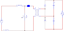
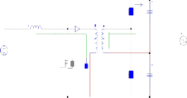
Fig. 1 shows the circuit topology of studied solar microinverter. The grid connected solar microinverter consists of isolated boost con- verter with a secondary voltage doublers and inverter circuit. Fig. 2 shows the modes of operation of grid connected solar microinverter with single stage boost conversion. According to the ac grid voltage the above circuit operates two modes they are explained below.
power as possible from the solar energy. PV energy systems are being extensively studied because of their benefits of envi- ronmental friendly and renewable characteristics. Typically, several PV panels are connected in series to provide a high-
PVpanel
L Cin\
Db
D D1
T1
Q
C1
L02
Co Grid
voltage output.
————————————————
C2 S2 S4
Lb
Qb
• P.Jeyankondan is currently pursuing masters degree program in power elec- tronics and drives in Anna University, India, E-mail: jeyaporkodi@gmail.com
• V.Hemamageswari –Assitant professor-Sethu Institute of Technology, India,. E-mail: hemanthinihema@gmail.com
• Dr M. Santhi-Professor and Head Of the Department Electrical&Electronics
Engineering -Sethu Institute of Technology, India.
Fig.1. Circuit diagram
Mode 1: When the grid voltage is higher than a boundary voltage Vb expressed as equation (1), solar microinverter is operated under this mode
IJSER © 2014 http://www.ijser.org
![]()
International Journal of Scientific & Engineering Research, Volume 5, Issue 4, April-2014 1100
ISSN 2229-5518
![]()
L D
T1 D1 C1
. (1)
Vg
(4)
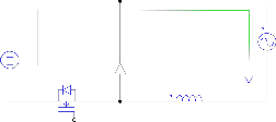
Fig. 3 and Fig. 4 respectively shows the equivalent circuits of studied solar microinverter under mode 1 and mode 2.
State 1(tR0R -tR 1R): During this time interval, power MOSFET Q ON, and diodes DR1R and DR2R are off. The solar energy is stored into input induc- tor L. The load energy is provided by voltage doubler capacitors CR1Rand CR2R.
State 2(t -t ): During the interval, power MOSFET Q is turned off.
R1R
R 2R
Vpv
Lb
Vpv
Q
D2
C2
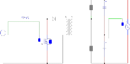
(a)Mode1
Db
Grid
The solar energy stored in inductor L is released via transformer T
and diodes DR1R, DR2R.
Mode 2: This mode for isolated solar microinverter can be divided
into two switching states.
State 1(tR0R-tR 1R ): During the time interval, power MOSFET QRbR is on and diode DRbR is off. The solar energy is stored into buck inductor LRbR . The voltage across LRbR can be expressed as follows:
![]() (5)
(5)
State 2(tR1R -tR 2R): At tR1R, power MOSFET QRb Ris turned off. The solar en- ergy stored in buck inductor LRbR is released via diode DRb. R The voltage across LRbR can be expressed as follows:
![]() (6)
(6)
Qb Lb
(b)Mode 2
Fig.2. Modes of operation
Where n is the turns ratio of transformer TR 1R,δRboostminR is the mini- mum duty cycle of boost switch Q and VRpvR denotes the PV panel voltage . PV panel voltage VRpvR is directly fed to the boost converter. Under this operation mode, the buck switch QRbR is always on the duty cycle δRboost. RQ is modulated as equation (2) to provide a rectified si- nusoidal waveform ׀Vg׀R. RCR1R and CR2R are connected with the AC grid system via inverter and LC output filter. Because the inverter is oper- ated at the Zero crossing of the AC grid voltage, the switching losses are neglected. Assuming that the conduction loss on power devices of the inverse buck and inverter can be ignored, the only loss of studied solar micro inverter is due to the single stage power conversion of the isolated boost converter circuit. High conversion efficiency can thus be achieved, i.e.,
![]() (2)
(2)
Mode 2: When the ac grid voltage is lower than the boundary voltage VRbR, the solar micro inverter is operated under this mode. The duty cycle δRboostR of Q is fixed at the minimum value δRboost,minR to provide a constant voltage gain KRbR as follows:
Vpv
T1 D1
L D C1
Vg
Q
D2 C2
(a)Mode 1 state 1
T1 D1
L D C1
Vg
Vpv Q
D2 C2
![]()
(3)
The duty cycle δRbuck R of buck switch QRbR is modulated as equation (4) to provide a rectified sinusoidal waveform ׀VRgR ׀ on capacitors CR1R and CR2R that is connected with the ac grid system via inverter and LC filter., i.e.,
(b)Mode 1 state 2
Fig. 3. Mode 1 operating states
IJSER © 2014 http://www.ijser.org
International Journal of Scientific & Engineering Research, Volume 5, Issue 4, April-2014 1101
![]()
ISSN 2229-5518
Vpv
Db
Grid
where Ts is the switching period of power MOSFET Qb.
(11)
Vpv
Qb Lb
(a)Mode 2 State 1
Grid
Db
The simulations were realized with a PV panel voltage of 25 V, a grid voltage of at 50 Hz and a switching Frequency of 20 KHZ. The bus capacitors were formed by two 3 mF capacitors connected in series. The output filter was formed by two inductors and a capacitor. The value of output capacitor is 2.2 mF. The output inductors values are 2.5mH. The inverter stage is formed by four (S1 to S4) switches. They are able to generate 230V, 50 HZ ac supply.
The simulation output of the PV panel. The PV panel de- sign is simulated for 25V
Qb Lb
(b)Mode 2 State 2
Fig.4. Mode 2 operating states
According to the waveforms shown in Fig .9 , the voltage stresses on power MOSFET Q can be represents as follows:
![]() (7)
(7)
Where Vg,pk denotes the peak value of the ac grid voltage. The trans- former turns ratio is usually set higher than unity; therefore low volt- age stresses on Q can be achieved. With low voltage stress on Q can be achieved. With low-voltage-rating devices for Q, low ON-state resistance Rds(on) can significantly reduce the conduction losses. The voltage stresses for diodes D1 and D2 and capacitors C1 and C2 can be determined by![]()
![]() (8) Considering the current ripple amount ΔIL, the inductance L can be calculated by
(8) Considering the current ripple amount ΔIL, the inductance L can be calculated by
Fig.5 switching pulse for boost switch
Fig.5 shows the switching pulse of boost switch. X axis denotes the time period, Y axis denotes duty ratio.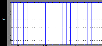
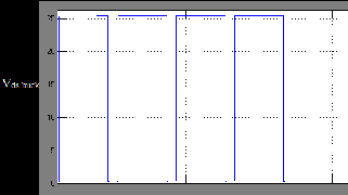
Fig.6 switching pulse for buck switch
Fig.6 shows the switching pulse of buck switch. X axis denotes the time period, Y axis denotes duty ratio.
Where Ts is the switching period of power MOSFET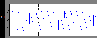
(9)
B. Inverse-Buck Circuit
The voltage stresses on power MOSFET Qb and diode Db
can be represented as follows:![]()
(10)
With low-voltage-rating devices for Qb and Db, high conversion efficiency can be achieved due to low conduction losses.
Considering the current ripple amount ΔILb, the inductance of
Lb can be calculated by
Fig.7 voltage doubler output
Fig.7 shows the simulation output of the voltage doubler output voltage. X axis denotes time period, Y axis denotes Vvd volt- age doubler output voltage.
IJSER © 2014 http://www.ijser.org
International Journal of Scientific & Engineering Research, Volume 5, Issue 4, April-2014 1102
ISSN 2229-5518
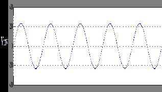
Fig.8 Inverter output
Fig.8 shows the output voltage of inverter. The inverter circuit consists of 4 switches S1-S4 . Its output voltage depends on the volt- age doubler output. In Y axis denote Vinv inverter output voltage.
(b) Buck switch
Fig.10 voltage across the boost and buck switches
TABLE I
LIST OF SYMBOLS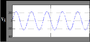
.
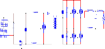
Fig .9 Grid voltage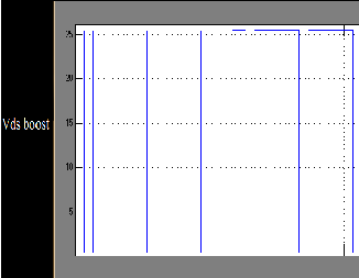
Fig .9 shows the grid voltage of the grid connected circuit. Generally PV inverters are connected with distributed generation such as lighting loads for commercial and domestic purpose. In Y axis denotes Vg grid voltage.
(a)Boost switch
Fig.10a shows the switching pulse of the boost switch Q . In Y axis denotes Vds boost drain to source voltage and fig.10b shows the switching pulse of the buck switch. In Y axis denotes Vds boost drain to source voltage and the duty cycle of the Q and Qb depends on the modes of operation and output voltage of the inverter.
This topology dealt with a transformer isolated single phase grid connected microinverter for photo voltaic system. The grid connected solar microinverter based on single stage conversion circuit gives the
230V ac for 25V PV panel input voltage. This circuit stabilizes the output voltage by the feedback switching circuit. The topology reduc- es the number of switches required. Here the voltage doubler circuit increases the output voltage of the converter circuit. LCL filter gives the pure form of output voltage without disturbances. Thus the grid connected solar microinverter based on single stage boost conversion is simulated. Future work is focused on switching pulse generated by SPWM.
IJSER © 2014 http://www.ijser.org
International Journal of Scientific & Engineering Research, Volume 5, Issue 4, April-2014 1103
ISSN 2229-5518
[1] [1 M. J. V. Vazquez, J. M. A. Marquez, and F. S. Manzano,“A meth- odology for optimizing stand-alone PV-system size using parallel- connected dc/dc converters,” IEEE Trans. Ind. Electron., vol. 55, no. 7, pp. 2664–2673, Jul. 2008.
[2] J. H. Lee, H. S. Bae, and B. H. Cho, “Resistive control for a photovol- taic battery charging system using a microcontroller,” IEEE Trans. Ind. Electron., vol. 55, no. 7, pp. 2767–2775, Jul. 2008.
[3] X. Weidong, N. Ozog, and W. G. Dunford, “Topology study of pho- tovoltaic interface for maximum power point tracking,” IEEE Trans. Ind. Electron., vol. 54, no. 3, pp. 1696–1704, Jun. 2007.
[4] J. H. Park, J. Y. Ahn, B. H. Cho, and G. J. Yu, “Dual-module-based
maximum power point tracking control of photovoltaic systems,”
IEEE Trans. Ind. Electron., vol. 53, no. 4, pp. 1036–1047, Jun. 2006.
[5] M. Fortunato, A. Giusti niani, G. Petrone, G. Spagnuolo, and M. Vitell i ,
“ Maxi mum power poi nt tracki ng in a one-cycl e-control l ed singl e-stage pho-
tovoltai c i nverter,” IEEE Trans. Ind. Electron., vol. 55, no. 7,pp. 2684–2693, Jul. 2008.
[6] N. Mutoh and T. Inoue, “ A control method to charge seri es-connected ultra
el ectri c double-layer capacitors suitable for photovoltai c generati on systems combi ni ng MPPT control method,” I EEE Trans. Ind. Electron.,vol. 54, no.
1, pp. 374–383, Feb. 2007.
[7] . Bacciarell i, G. Lucia, S. Saponara, L. Fanucci, and M . Forli ti, “ De- si gn,testi ng and prototypi ng of a software programmabl e I2C/SPI IP on AMBA bus,” i n Proc. Ph. D. Res. Microelectron. Electron., Jun. 2006,pp.
373–376.
[8] J. T. Bialasi ewicz, “ Renewabl e energy systems with photovoltai c power generators: Operation and model ing,” IEEE Trans. Ind. Electron., vol .
55,no. 7, pp. 2752–2758, Jul. 2008.
[9] M. Bertoluzzo and G. Buja, “ Devel opment of el ectri c propul si on systems for light electri c vehicles,” IEEE Trans Ind. Informat., vol. 7, no. 3,pp. 428–
435, Aug. 2011.
[10] M. P. Kazmi erkowski, M . Jasi nski, and G. Wrona, “ DSP-based control of gri d-connected power converters operati ng under gri d di storti ons,” IEEE Trans Ind. Informat., vol. 7, no. 2, pp. 204–211, May 2011.
[11] Y. S. Lai, C. A. Yeh, and K. M. Ho, “ A famil y of predi cti ve di gital con-
trol led PFC under boundary current mode control,” IEEE Trans.Ind. Infor- mat., vol. 8, no. 3, pp. 448–458, Aug. 2012.
[12] S. Dasgupta, S. N. M ohan, S. K. Sahoo, and S. K. Panda, “ A plug and play
operational approach for i mpl ementation of an autonomous-microgri d sys- tem,” IEEE Trans. Ind. Informat., vol. 8, no. 3, pp. 615–629,Aug. 2012.
[13] H. H. Wu, A. Gil chri st, K. Seal y, and D. Bronson, “ A high effi ci ency5 kW
inductive charger for EVs usi ng dual si de control,” I EEE Trans.Ind. Infor- mat., vol. 8, no. 3, pp. 585–595, Aug. 2012.
[14] G. Buticchi , D. Barater, E. Lorenzani , and G. Franceschi ni, “ Di gi tal control of actual gri d-connected converters for ground leakage current reduction i n
PV transformerl ess systems,” I EEE Trans. Ind. Informat., vol. 8, no. 3, pp.
563–572, Aug. 2012.
[15] Huang-Jen Chiu, Senior Member, IEEE, Yu-Kang Lo, Member, I EEE, Chun-
Yu Yang, Shi h-Jen Cheng,Chi -Mi ng Huang, Chi ng-Chun Chuang, Mi n- Chi en Kuo, Yi -Mi ng Huang, Yuan-Bor Jean, and Yung-Cheng Huang“ A Modul e-I ntegrated I solated Solar Mi croi nverter” , . IEEE Trans. Ind. Elec- tron., vol. 60,no. 2., Feb. 2013.
[16] R. Mastromauro and M. Dell Liserre, “A control issues in single-stage photovoltaic systems: MPPT, current and voltage control,” IEEE
Trans Ind. Informat., vol. 8, no. 2, pp. 241–254, May 2012.
[17] T. Hirose and H. Matsuo, “Standalone hybrid wind–solar power
generation system applying dump power control without dump
load,” IEEE Trans. Ind. Electron., vol. 59, no. 2, pp. 988–997, Feb. 2012. [18] S. Jiang, D. Cao, D. Y. Li, and F. Peng, “Grid-connected boost-half
bridge photovoltaic micro inverter system using repetitive current control and maximum power point tracking,” in Proc. 27th Annu. IEEE (APEC),Feb. 2012, pp. 590–597.
[19] R. J. Wai and C. Y. Lin, “Dual active low-frequency ripple control for clean-energy power-conditioning mechanism,” IEEE Trans. Ind. Elec- tron.,vol. 58, no. 11, pp. 5172–5185, Nov. 2011.
[20] N. Femia, G. Petrone, G. Spagnuolo, and M. Vitelli, “Distributed
maximum power point tracking of photovoltaic arrays: Novel ap-
proach and system analysis,” IEEE Trans. Ind. Electron., vol. 55, no. 7, pp.2610–2621, Jul. 2008.
[21] J. M. Carrasco, L. G. Franquelo, J. T. Bialasiewicz, E. Galvan,R. C.
Portillo-Guisado, M. A. M. Prats, J. I. Leon, and N. Moreno-Alfonso,
“Power-electronic systems for the grid integration of renewable en- ergy sources: A survey,” IEEE Trans. Ind. Electron., vol. 53, no. 4, pp.
1002–1016, Jun. 2006.
[22] A.Al Nabulsi and R. Dhaouadi, “Efficiency optimization of a DSP-
based standalone PV system using fuzzy logic and dual-MPPT con-
trol,” IEEE Trans Ind. Informat., vol. 8, no. 3, pp. 573–584, Aug. 2012 [23] B. Sahan, A. N. Vergara, N. Henze, A. Engler, and P.Zacharias, “A
single stagePV module integrated converter based on a low-power current source inverter,” IEEE Trans. Ind. Electron., vol. 55, no. 7, pp.
2602–2609,Jul. 2008.
[24] A.Y. Sendjaja and V. Kariwala, “Decentralized control of solid oxide fuelcells,” IEEE Trans I nd. Informat., vol. 7, no. 2, pp. 163–170, May
2011.
IJSER © 2014 http://www.ijser.org