International Journal of Scientific & Engineering Research, Volume 6, Issue 3, March-2015 34
ISSN 2229-5518
Generation of UWB Waveforms with
Adaptive Mitigation of Multiple Narrowband
Interference in IR-UWB Systems
Haydar M. AL-Tamimi * and Hussein Ali Hamza **
Abstract: - One of the main types of waveforms adopted by ultra wideband (UW B) system is Gaussian pulse in addition to other types of waveforms such as raised cosine pulse and Hermite pulse. Spectrum shaping in impulse radio ultra wideband (IR-UW B) network is a straightforward way for modifying the Power Spectral Density (PSD) of the emitted signal in order to meet the limitations set by Federal Communications Commission (FCC) spectral masks for indoor and outdoor environments. Due to overlapping frequency bands, Narrowband (NB) (W iMAX, W LAN) and UW B systems. UW B signals suffer from multiple NB interferers with varying powers, which lead to a severe performance degradation. A combination waveforms consists a sum of 4th-
4th, 5th-5th, and 4th-5th order derivative of Gaussian pulses with time delay interval between them for adaptive mitigation of multiple NB interference in IR-UW B systems has been presented in this work. This can be achieved by inserting frequency notches into the IR-UW B power spectrum at center frequency of narrowband signals to limit interference. The design and simulation of the pulse generators (PGs) was performed using Advanced Design System (ADS) in 0.25 µm RF CMOS process.
Keywords— UW B, Pulse generator, Gaussian Pulse, FCC.
—————————— ——————————
1. Introduction
R-UWB system, a very short pulses (generally 0.1 → 1
ns) are used to transmit information symbol, which
spread energy of the signal of frequency up to 10 GHz [1]. The power spectral density (PSD) of transmitted pulses must satisfy power and spectrum limits of the Federal Communications Commission (FCC) spectral mask [2]. A UWB system is defined as any radio system that has fractional bandwidth (FB) larger than 20% of its center frequency, or has a -10 dB bandwidth equal to or greater than 500 MHz, regardless of the FB.
2. Design Waveforms Meet the FCC Spectral
Mask
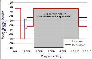
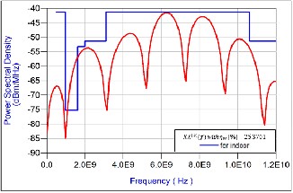
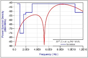
The FCC spectral mask assigned for indoor communications is shown in Figure (1). It’s clear that most of the power should be allocated to the band 3.1 – 10.6
GHz, also to avoid interference to narrowband system for
frequencies less than 3.1 GHz.
Different types of pulse shape are used to meet the
requirements of FCC spectral mask [3-5]. The most commonly used pulses are derivation of Gaussian monocycle and modified Hermite pulses (MHP) [6-8].

*Dr. Haydar M. AL-Tamimi, Electrical Engineering Department, University of Technology, Baghdad, Iraq,
**Eng. Hussein Ali Hamza, Electrical Engineering Department, University of Technology, Baghdad, Iraq,
E-mail: hn_karbala@yahoo.com
Figure (1) FCC spectral mask for indoor and outdoor UW B
communications
3. How to Compare between PSD of a
Waveform with FCC spectral masks
In order to make a robust comparison between the PSD of any proposed pulse with FCC spectral mask, several of comparison parameters have been used. The work in [9], used the PSD efficiency (usually referred by
𝜂𝑃 ), which is defined as the ratio of the PSD of any pulse
to the FCC spectral mask as shown below [10]:
IJSER © 2015 http://www.ijser.org
International Journal of Scientific & Engineering Research, Volume 6, Issue 3, March-2015 35
ISSN 2229-5518
where 𝑡 is the time, 𝜎 is the pulse width parameter which
is used to adjus𝑓t=t1h0.e6𝐺p𝐻𝑧ulse width 𝑇𝑃 and A is constant
amplitude.
The nth derivative � Ga 𝜙𝑢 (𝑓) pulse is given as [10, 11]:
of

𝜂 = 𝑓𝐿 =3.1𝐺𝐻𝑧

𝑓 =10.6𝐺𝐻𝑧
ussian
× 100% (1)
𝐻 2
𝑛 −
(𝑛−2)
(𝑛−1)
𝑥(𝑡) = �− 𝜎2 �(𝑃𝐹𝐶𝐶 (1𝑓))𝑥
𝑓𝐿 =3.1𝐺𝐻𝑧
(𝑡) + 𝑡𝑥
(𝑡)� (4)
where 𝜙𝑛 (𝑓) is PSD of the pulse and 𝐹𝐶𝐶(𝑓) is the FCC
spectral mask. High value of 𝜂𝑃 means high value of
The amplitude of the Fourier transform of the nth
derivative of Gaussian pulse can be expressed as [10, 11]:
received power. The disadvantage of this method appears
when a violation region of 𝜙𝑛 (𝑓) to 𝐹𝐶𝐶(𝑓) is appeared
𝑋𝑛 (𝑓) = 𝐴(𝑗2𝜋𝑓)𝑛
∙ exp[−(𝜋𝑓𝜎)2 ] (5)
which leads to inaccurate result, thus Equation (1) is
useful under condition of no violation.
Another parameter of comparison is used by [10], which is based on principle of least square error (LSE) to
minimize the deviation between 𝜙𝑛 (𝑓)and𝐹𝐶𝐶(𝑓). Error
parameter can be expressed by [10]:
Thus the amplitude spectrum of the nth order derivative
is [10, 11]:
|𝑋𝑛 (𝑓)| = 𝐴(2𝜋𝑓)𝑛 ∙ exp[−2(𝜋𝑓𝜎)2] (6)
The work in [12] show that the 5th order derivative of
Gaussian pulse meets the regulatory requirements of
𝑓𝐻 =10.6𝐺𝐻𝑧
FCC for indoor case, while 7th order derivative meets the
requirem 𝐸 =for � td
|𝜙𝑢 (𝑓) − 𝑃𝐹𝐶𝐶 (𝑓)|2𝑑𝑓
(2)
ents
ou oor case.
In the case when there is large amount of violation, 𝐸 can be more useful than 𝜂𝑃 when the goal is to approach
numerically best proposed pulse that meets the FCC
requirement. Although, of that, E is not active always.
4. Parameters Used for Comparison Purpose
A parameter has been used in this work referred to
matching efficiency 𝜂𝑀 which gives the degree of
matching to FCC spectral mask. This parameter is useful
in both cases with and without violating FCC limits. The
matching efficiency can be expressed as follows [10]:

1 − ∑|𝑑𝑖 |
𝑓𝐿 =3.1𝐺𝐻𝑧
6. Interference from Other Radiators to UWB
Systems
Initially, the main concern about UWB was whether or not they would interfere with existing RF systems that provide essential military, aviation, fire, police, and rescue services. For such a reason, the FCC spent about two years evaluating the proposed UWB specifications and concluded that there should be no major interference from the UWB systems. This conclusion is made mainly because of the extremely low emission power limitation on the UWB system [13].
But on the other hand, low powered UWB equipment's themselves are facing significant interference problem
where
𝜂𝑀 =
∑ 𝐹𝐶𝐶𝑖
× 100% (3)
from other wireless systems. Among them, WiMax and
802.11a WLAN. Where WiMax band is less than -
𝑑𝑖 = ∅𝑛 (𝑓)𝑖 − 𝐹𝐶𝐶𝑖 (4)
where 𝐹𝐶𝐶𝑖 is the FCC spectral value at point 𝑖 and ∅𝑛 (𝑓)𝑖
is the PSD of the transmitted pulse at point 𝑖.
The comparison parameters in Equations (3) (and also the
-10 dB bandwidth) will be adopted in this work in all
comparisons will be made between PSD of the proposed
waveform and FCC spectral mask of indoor environment.
5. Gaussian Pulse
The general form of Gaussian pulse is given by [11, 12]:
80dBm/MHz at center frequency 3.5 GHz, and 802.11a
WLAN system is the main concern.
Because it has a high emission power at center frequency
5.25 GHz is inside of the FCC approved operating band for UWB systems as shown in Figure (2) and (3). Therefore, in the following section studied the problem of interference from 802.11a WLAN to UWB system [13].
𝐴

𝑥(𝑡) =
√2𝜋𝜎
exp �−

𝑡 2
2𝜎2
� (3)
IJSER © 2015
http://www.ijser.org
International Journal of Scientific & Engineering Research, Volume 6, Issue 3, March-2015 36
ISSN 2229-5518
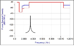
Figure (2): W iMax power spectrum at center frequency 3.5GHz
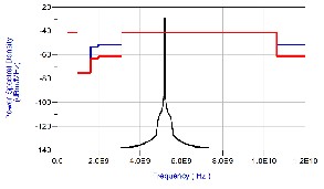
Figure (3) W LAN power spectrum at center frequency 5.25GHz.
7. Solution to the Interference Problem
As shown in the simulation result and stated above, WLAN interference signal is the killer to UWB system, and the solution needs to be found out to allow UWB system operating with a nearby 5GHz WLAN interference source. Spectrum shaping, is another method to mitigation of NBI. In this work suppression for the NBI of Unlicensed National Information Infrastructure (U-NII) system can be done by inserting a notch in the spectrum of transmitted waveform at
𝑓𝑛𝑜𝑡𝑐ℎ𝑒 = 5.25 GHz, A proposed circuit for combination
of Gaussian pulses with time delay difference between
them will be described to produce a waveform that can give better performance for NBI reduction [13].
8. Waveform design for NBI Mitigation
When looking to generate UWB pulse signals many different pulse waveforms may be used. In the work [14,15] a method is used to eliminate interferences with NB system. By using sum of two identical order of
derivative (and also identical 𝜎) Gaussian pulses with δ
time delay difference between them as shown in figure
(4). The composite UWB waveform resulting from sum of
two identical Gaussian pulses referred to in this work
by 𝑥𝑥(𝑛) (𝑡)[10,15]:
𝑥𝑥(𝑛) (𝑡) = A1 . 𝑥(𝑛) (𝑡) + A2 . 𝑥(𝑛) (𝑡 − δ ) (7)
where A1 and A2 are the amplitudes of the original pulse
and the delayed pulse, respectively. In the ideal case the
two pulses have identical shapes and amplitudes (A1
=A2). Difference is a short relative time delay δ between
the two pulses. Based on this 𝑥𝑥(𝑛) (𝑡) .where n is the
order of derivative and its Fourier transform referred
by 𝑋𝑋 (𝑛) (𝑓).The Fourier transform of sum of two n
derivative Gaussian pulses separated by δ time delay
can be expressed by [10]:
�𝑋𝑋 (𝑛) (𝑓)� = �𝑋 (𝑛) (𝑓)� ∙ |1 + exp(−𝑗2𝜋𝑓𝛿)| (8)
where �𝑋(𝑛) (𝑓)� is given by Equation (6), this leads to
[10]:
�𝑋𝑋(𝑛) (𝑓)� = 𝐴(2𝜋𝑓)𝑛 ∙ exp[−(2𝜋𝑓𝜎)2 ]
∙ |1 + exp(−𝑗2𝜋𝑓𝛿)| (9)
The PSD of the composite Gaussian waveform depends
on three parameters n, 𝜎 and 𝛿. To find the optimum
values of these parameters, an optimization method
needs to be used.
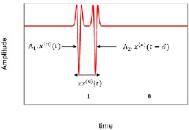
Figure (4): The combination of two pulses with a relative time delay δ
For NBI Mitigation.
A block diagram of the simulation of the proposed method is shown in Figure (5), tow high order derivative
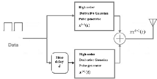
Gaussian PG 𝑥(𝑛) (𝑡) and time delay 𝛿 block are for generating the composite waveform 𝑥𝑥(𝑛) (𝑡) and time delay 𝛿 in Equation (7), respectively.
IJSER © 2015 http://www.ijser.org
International Journal of Scientific & Engineering Research, Volume 6, Issue 3, March-2015 37
ISSN 2229-5518
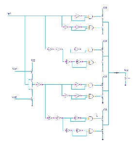
Figure (5): The block diagram illustrating the simulation of the proposed frequency notching method.
The time delay block can be realized by CMOS time delay cells, which can provide fine delay time in the
order of hundreds of ps [15].
A composition of two Gaussian waveforms of identical
order of derivative with time delay interval between them can be used for mitigating interference from NB systems. The NBI suppression can be done by inserting a notch in the spectrum of the transmitted waveform. The spectrum of two n derivative Gaussian pulses separated by δ time delay is defined by Equation (8). The minimum values of the spectrum of Equation (8) represent notches occur at frequencies that satisfy the following Equation [10, 14, 15]:
𝑘 + 1
𝑓𝑛𝑜𝑡𝑐ℎ𝑒𝑠 = 2 , 𝑘 = 0, 1, 2, ⋯ (10)
𝛿
where 𝑓𝑛𝑜𝑡𝑐ℎ𝑒𝑠 can be used as the center frequency of the
required suppressed band. According to Equation (10)
the required time delay δ can be found for a
proper𝑓𝑛𝑜𝑡𝑐ℎ𝑒𝑠. Therefore, the suppression for the NBI of
Unlicensed National Information Infrastructure (U-NII)
system can be done by inserting a notch in the spectrum
of transmitted waveform at 𝑓𝑛𝑜𝑡𝑐ℎ𝑒𝑠 = 5.25 GHz. In
following sections, different combined waveforms have
been generated in order to mitigate the NBI of U-NII system. The optimization process has been modified to generate the optimum combined waveforms having PSD contains a notch at center frequency of U-NII system and also meets the FCC requirements for indoor and outdoor environments.
Figure (6) block diagram schematic for combination of 5th-5th derivative
Gaussian PG.
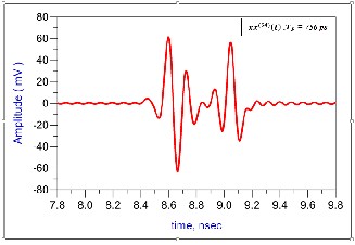
Simulation results of 𝑥𝑥 (5) (𝑡) PG circuit are shown in Figures
(7) and (8), these Figures illustrates ADS plot of the optimum
𝑥𝑥(5) (𝑡) waveform and it's PSD. Thus by adjusting the time
delay between two identical pulses frequency notches can be
inserted. When using 𝛿 = 0.562𝑛𝑠 the third frequency notch
is inserted at 5.25 GHz to mitigate the NBI of U-NII system.
In addition, other notches are located at (0.96, 3.15, 7.2, 9.3,
11.3) GHz, as shown in Figure (8).
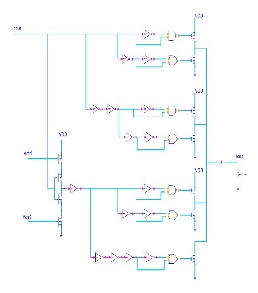
9. Generating composite UWB waveform
𝒙𝒙(𝟓) (𝒕) for NBI Mitigation
Combining the two circuit blocks, 5th derivative
Gaussian PG and 5th derivative Gaussian PG plus delay
block and as shown Figure (6).This block diagram schematic for composition of two 5th derivative Gaussian pulse with δ time delay interval between them. By using two ways leading to varying delay time as desired, the first one by adding series of inverter for changing delay time. The second, delay circuit reported in [15] consist of only a few small-sized inverters. And this Delay circuit, which has two biasing voltages, to provide the possibility of adaptive tuning of the notched frequencies, more details about delay circuit in [16], and the second way is the best. 5th derivative Gaussian PG are similar to the one described in [12], which is composed of delay stage and a simple NOR/NAND gate.
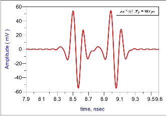
Figure (7): zoomed view of output for combined 𝑥𝑥
time delay δ.
(5)(𝑡)
waveform with
IJSER © 2015 http://www.ijser.org
International Journal of Scientific & Engineering Research, Volume 6, Issue 3, March-2015 38
ISSN 2229-5518
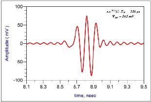
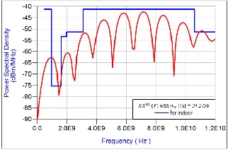
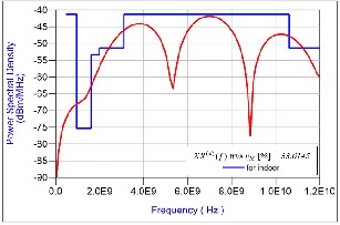
Figure (8): PSDs of 𝑥𝑥 (5) (𝑡) with 𝛿 = 0.562𝑛𝑠 for multiple NBI Mitigation
purpose used for indoor case.
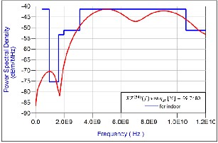
The time delay δ of the generated waveform can be
computed by substituting 𝑓𝑛𝑜𝑡𝑐ℎ𝑒𝑠 = 5.25 GHz in Equation
(10) and then Equation (7) is used to generate 𝑥𝑥 (𝑛) (𝑡)
waveform. It is found that 5 is the minimum order of
derivative of 𝑥𝑥(𝑛) (𝑡) waveform that produces PSD
satisfying the indoor FCC mask and also contains a notch
at 𝑓 = 5.25 GHz. Figure (10) shows the PSD of 𝑥𝑥(5) (𝑡).The
time delay of PSD in Figure (10) is calculated using
Equation (10) with 𝑓 = 5.25 GHz and 𝑘 = 0 which equals to 95 ∗ 10−12. It is clear that 𝑘 + 1 represents number of
notches in the spectrum of the waveform, thus as the best
value of k is zero which gives only one notch at the required frequency.
Accordingly,𝑥𝑥 (5) (𝑡), is the best choice for producing
PSD satisfying the NBI mitigation. The optimum 𝑥𝑥(5) (𝑡)
waveform can be expressed by [10, 14, 15]:
Figure (9): zoomed view of output for combination 𝑥𝑥 (5) (𝑡) derivative of
Gaussian pulse with time delay δ = 0.094𝑛𝑠.
Figure (10): PSD of 𝑥𝑥 (5) (𝑡) with 𝛿 = 0.094𝑛𝑠 used to mitigate interference effect of U-NII system.
By changing the time delay between two identical pulses of 5th order, frequency notches can be inserted at desired
frequen𝑥ci𝑥e(s5)a(s𝑡)sh=ao𝑥w(5n) (𝑡in) +th𝑥e(n5)e(x𝑡t−fi9g5ur∗e1s.0−12 ) (11)
where 𝑥(5) (𝑡) with 𝜎 = 53.532 ps can be expressed by [12].
∙ 2)
The waveform of Equation (11) is plotted in Figure (9).
When V ctr1 and V ctr2 are 1.11 V and 0.442 V
respectively, the frequency notches are located at 𝑓 =
5.25 GHz, which are very close to those in Figure (10)
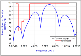
Figure (11): PSD of 𝑥𝑥 (5) (𝑡) with 𝛿 = 0.323𝑛𝑠 for NBI Mitigation purpose
used for outdoor case.
IJSER © 2015 http://www.ijser.org
International Journal of Scientific & Engineering Research, Volume 6, Issue 3, March-2015 39
ISSN 2229-5518
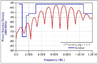
Table (1) Summarize of the frequency notching of 𝑥𝑥 (5) (𝑡) PG
Figure (12): PSD of 𝑥𝑥 (5) (𝑡)with 𝛿 = 0.812𝑛𝑠 for multiple NBI Mitigation
for indoor case.
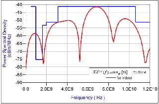
Figure (13): PSD of 𝑥𝑥 (5) (𝑡)with 𝛿 = 0.666𝑛𝑠 for multiple NBI Mitigation for indoor case.


Figure (14𝑥):(4P)S(𝑡D) o=f 𝑥𝑥 (5) (�𝑡)wi−th 𝛿 = +0.385�𝑛𝑠∙ efxorpm�u−ltiple N�BI Mitigati(o1n4. )
Table (2) Comparison parameters of PSDs of 𝑥𝑥 (5) (𝑡) PG.
10. Generating composite UWB waveform
𝒙𝒙(𝟒) (𝒕) for NBI Mitigation
based on the same concept in section 9, Combining the
two circuit blocks, 4th derivative Gaussian PG and 4th
derivative Gaussian PG plus delay block and as shown Figure (15).This block diagram schematic for composition of two 4th derivative Gaussian pulse with δ time delay interval between them.
For the combination of 4th- 4th 𝑥𝑥(4) (𝑡) which can be
expressed by:
𝑥𝑥(4) (𝑡) = 𝑥(4) (𝑡) + 𝑥 (4) (𝑡 − δ ) (13)
where 𝑥(4) (𝑡) is can be expressed by [12]:
√2𝜋
𝜎9
𝜎7
𝜎5
2𝜎2
In order to generate 𝑥𝑥(5) (𝑡) containing a notch at
𝑓 = 5.25 GHz to be used to mitigate interference effect of
U-NII system in addition to meet the indoor FCC mask
requirements. Table (1) Summarize the values of 𝛿 and
number of notches and its locatoins. The results given in
Table (1) are obtained by changing parameters 𝑉𝑐𝑡𝑟1 , 𝑉𝑐𝑡𝑟2.
The Comparison parameters of PSDs of combined
waveforms in previous Figures are given in Table (2)
IJSER © 2015 http://www.ijser.org
International Journal of Scientific & Engineering Research, Volume 6, Issue 3, March-2015 40
ISSN 2229-5518
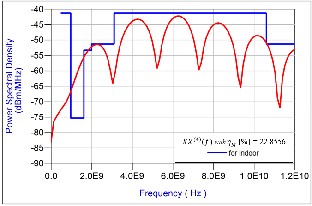
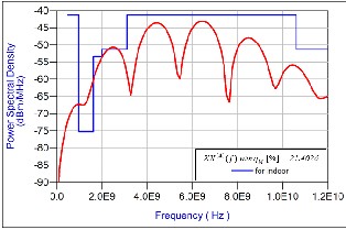
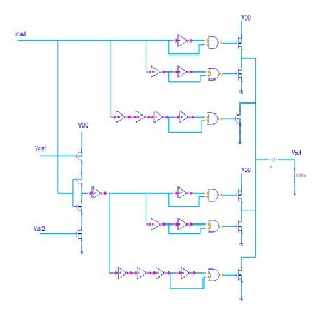 Figure (17): PSD of 𝑥𝑥 (4) (𝑡)with 𝛿 = 0.437𝑛𝑠 for multiple NBI Mitigation.
Figure (15) block diagram schematic for combination of 4th- 4th
derivative Gaussian PG.
Simulation results of 𝑥𝑥(4) (𝑡) PG circuit are shown in
Figures (16), these Figures illustrate ADS plot of the
optimum waveform 𝑥𝑥(4) (𝑡) .
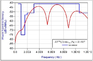
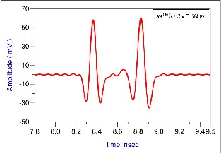 Figure (18): PSD of 𝑥𝑥 (4) (𝑡)with 𝛿 = 0.505𝑛𝑠 for multiple NBI Mitigation.
Figure (16) zoomed view of output for combination 4th-4th derivative of
Gaussian pulse with time delay δ.
By changing the time delay between two identical pulses of
4th order, frequency notches can be inserted at desired
frequencies as shaown in the next figures.
Figure (19): PSD of 𝑥𝑥 (4) (𝑡) with 𝛿 = 0.297𝑛𝑠 for NBI Mitigation purpose.
IJSER © 2015 http://www.ijser.org
International Journal of Scientific & Engineering Research, Volume 6, Issue 3, March-2015 41
ISSN 2229-5518
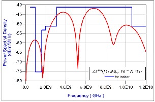 Table (4) Comparison parameters of PSDs of 𝑥𝑥 (4) (𝑡) PG
Figure (20): PSD of 𝑥𝑥 (4) (𝑡)with 𝛿 = 0.354𝑛𝑠 used to mitigate
interference effect of U-NII system.
Figure (21): PSD of 𝑥𝑥 (4) (𝑡) with 𝛿 = 0.224𝑛𝑠 for NBI Mitigation purpose.
11. Composite UWB waveform of Two Different
Gaussian Pulses
In the previous section, the optimum combination of two identical Gaussian pulses with time delay between them has been presented for indoor and outdoor system.
In this section of the work, a combination of two different
Gaussian pulses (with a time delay interval between them)
can be used to obtain a PSD with possibility of the interference mitigation from NB sources and meets the FCC requirements is discussed. The combined waveform resulting from sum of two different Gaussian pulses, referred to in this
work by 𝑥𝑥(𝑛𝑚) (𝑡), where n is the order of derivative of the
unshifted waveform while m is the order of derivative of the
(𝑛𝑚)
In order to generate 𝑥𝑥(4) (𝑡) containing a notches at 𝑓 = 5.25
shifted waveform and the Fourier transform 𝑥𝑥
(𝑛𝑚)
(𝑡)
GHz to be used to mitigate interference effect of U-NII
referred by 𝑋𝑋
(𝑓) can be expressed as follows [10]:
system in addition to meet the indoor FCC mask
requirements. Table (3) lists the optimum values of 𝛿. The
�𝑋𝑋
(𝑛𝑚)
(𝑓)� = �𝑋
(𝑛)
(𝑓)� + �𝑋
(𝑚)
(𝑓)� (15)
results given in Table (3) are obtained by changing
parameters 𝑉𝑐𝑡𝑟1 , 𝑉𝑐𝑡𝑟2. The Comparison parameters of PSDs
where
𝑋 (𝑛) (𝑓) is the Fourier transform of 𝑥(𝑛) (𝑡) and 𝑋 (𝑚) (𝑓)
(𝑚)
of combined waveforms in previous Figures are given in
is the Fourier transform of 𝑥
(𝑡)(𝑡 − 𝛿), By using the
Table (4).
Table (3): Summarize of the frequency notching of 𝑥𝑥 (4) (𝑡) PG.
spectrum of single Gaussian pulse given in Equation (6), the
amplitude spectrum of Equation (15) can be found as follows
[10]:
�𝑋𝑋 (𝑛𝑚) (𝑓)� = 𝐴[(2𝜋𝑓)𝑛 exp[−2(𝜋𝑓𝜎𝑛 )2 ]
+
(2𝜋𝑓)𝑚 exp[−2(𝜋𝑓𝜎𝑚 )2] ∙ exp(−𝑗2𝜋𝑓𝛿) ] (3.19)
where 𝜎𝑛 ≠ 𝜎𝑚 . If the two different Gaussian pulses have
equal orders(𝑛 = 𝑚), in such a case, the waveform is referred
to in this work by 𝑥𝑥(𝑛𝑛) (𝑡) and its Fourier transform by
𝑋𝑋 (𝑛𝑛) (𝑓).
IJSER © 2015 http://www.ijser.org
International Journal of Scientific & Engineering Research, Volume 6, Issue 3, March-2015 42
ISSN 2229-5518
12. Generating composite UWB waveform
𝒙𝒙(𝟓𝟒) (𝒕) for NBI Mitigation
Also, based on the same concept in sections 9-10,
Combining the two circuit blocks, 5th derivative Gaussian PG
and 4th derivative Gaussian PG plus delay block and as
shown Figure (22).This block diagram schematic for composition of two 5th-4th derivative Gaussian pulse with δ time delay interval between them. Delay circuit same as which mentioned in section 4.5.
Figure (22) block diagram schematic for combination of 5th-4th derivative
Gaussian PG.
Simulation results of 𝑥𝑥 (54) (𝑡) PG circuit are shown in Figures
(23), these Figures illustrate ADS plot of the optimum
waveform 𝑥𝑥(54) (𝑡).
Figure (23) zoomed view of output for combination 5th-4th derivative of
Gaussian pulse with time delay δ.
By adjusting the time delay between two pulses frequency notches can be inserted at desired frequencies. When using
𝛿 = 0.45𝑛𝑠 frequency notches are located at (1, 3.2, 5.25, 7.7,
10.4) GHz, more frequency notch are located which improves
compatibility with WiMax and WLAN. which are very close to those in Figure (24).
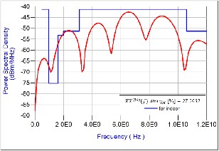
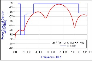
Figure (24): PSD of 𝑥𝑥 (54) (𝑡)with 𝛿 = 0.406𝑛𝑠 for multiple NBI Mitigation. Figure (25) PSDs of 𝑥𝑥 (54) (𝑡) with 𝛿 = 0.229𝑛𝑠 ps for NBI Mitigation
purpose used or indoor case.
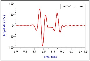
Figure (26): zoomed view of output for combination 𝑥𝑥 (54) (𝑡) waveform with time delay 𝛿.
IJSER © 2015 http://www.ijser.org
International Journal of Scientific & Engineering Research, Volume 6, Issue 3, March-2015 43
ISSN 2229-5518
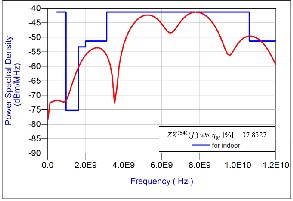
Figure (27): PSD of 𝑥𝑥 (54) (𝑡) waveform with 𝛿 = 0.255𝑛𝑠 for mitigate
interference effect of W iMax.
Figure (28): PSD of 𝑥𝑥 (54) (𝑡) waveform with 𝛿 = 0.073 𝑛𝑠.
In order to generate 𝑥𝑥(54) (𝑡) containing a notches at
𝑓 = 5.25 GHz and 𝑓 = 3.5 GHz to be used to mitigate
interference effect of U-NII and WiMax systems in
addition to meet the indoor FCC mask requirements.
Table (5) lists the optimum values of 𝛿. The results given
in Table (5) are obtained by changing
parameters 𝑉𝑐𝑡𝑟1 , 𝑉𝑐𝑡𝑟2. The Comparison parameters of
Table (7) Comparison parameters of PSD of 𝑥𝑥
13. Conclusion
(54) (𝑡)
in Figure (4.38).
PSDs of combined waveforms in previous Figures are
given in Table (6).
Table (5) Summarize of the frequency notching of 𝑥𝑥 (54) (𝑡) PG.
Table (6) Comparison parameters of PSDs of 𝑥𝑥 (54) (𝑡) PG.
It is possible to obtain better matching for Gaussian pulse PSD to meet FCC spectral mask by using sum of two high order of derivative Gaussian pulses with δ time delay interval between them as shown in Figure (28).
In this paper a method has been presented to generate different combined waveforms that can be used to adaptive Mitigation of Multiple Narrowband Interference in IR-UWB Systems and satisfy the requirements of FCC indoor spectral mask for UWB technology. These combined waveforms consist of two high order derivative (identical on not) Gaussian pulses with time delay interval between them. According to results in this work the following can be concluded, In case of using two identical Gaussian pulses, it can be concluded that 4th-4th and 5th-5th derivatives identical Gaussian pulses is the optimum pair of combined waveform that can used to Mitigation of Multiple Narrowband Interference in IR-UWB Systems and satisfy the requirements of FCC indoor spectral mask.
In case of using two different Gaussian pulses, it can be
concluded that the 5th-4th is the minimum order pair of
combined waveform that can be used to generate combined waveform with minimum violating to the limitations of FCC mask for indoor environment and Mitigation of Narrowband Interference.
As a suggestion for future work this method can be used to
generate combined waveforms that can meet the FCC emission mask for outdoor environments. Furthermore; this method can be used to generate other types of UWB regulations such as the European Conference of Postal and Telecommunications Administrations (CEPT) and Ministry of Internal Affairs and Communications (MIC) in Japan or regulations in other countries such as Korea and Singapore.
IJSER © 2015 http://www.ijser.org
International Journal of Scientific & Engineering Research, Volume 6, Issue 3, March-2015 44
ISSN 2229-5518
References
[1] Ranjit Gharpurey and Peter Kinget, “Ultra W ideband Circuit, Transceiver and Systems”, Springer, 2008.
[2] FCC, “First report and order, rules regarding ultra-wideband transmission system. Federal Communications Commission”, ET Docket, pp. 98-153, 2002.
[3] João A. Ney da Silva and Marcello L. R. de Campos, “Method for
Obtaining Spectrally Efficient Orthogonal UW B Pulse Shapes”,
International Telecommunications Symposium”, Fortaleza-CE
(Brazil), September 3-6, 2006.
[4] Ziaul Hasan, Vikas Yadav, A.K Chaturvedi and Vijay K. Bhargava, “Design of a family of ISI free pulses for very high data rate UW B
Wireless Systems”, IEEE 2007.
[5] Parinya Prommasuksakul, Pichaya Supanakoon and Sathaporn Promwong, “Power Spectral DensitY of UW B PSM Signal”, ThammasatI nt. J. Sc. Tech., Vol. 12, No. 4, October-December
2007.
[6] Srinivasu Maddula and Saswat Chakrabarti, “ Synthesis of UW B Pulse Following FCC mask”, 2005.
[7] W en Hu and Guoxin Zheng, “Orthogonal Hermite Pulses Used for UW B M-ary Communication”, Proc. of the Conference on Information Technology: Coding and Computing, IEEE 2005.
[8] Maria-Gabriella Di Benedetto and Luca De Nardis, “Tuning UW B Signals by Pulse Shaping: towards Context-Aware W ireless Networks”, Elsevier, 2006.
[9] Maddula, S. Chakvabarti, “Synthesis of UW B pulse following FCC
mask”, Proc. Union Radio Science General, 2005.
[10] Haydar Malik Abdulhadi, “Modified Pulse Shaping and Path Loss Modeling for UW B”, PhD Thesis, University of Technology, Electrical and Electronic Engineering Department, 2011.
[11] H. Sheng, P. Orlik, A. M. Haimovich, L. J. Cimini, and J. Zhang, “On the spectral and power requirement for Ultra-wideband
transmission”, Proc., IEEE Int. cont. communications, vol. 1, p. 738-
742, 2003.
[12] Hussein Ali Hamza, “Design of CMOS IR-UW B Transmitter”, in the
first international Conference on engineering sciences ̓ Applications,
ICESA, college of engineering, University of Karbala, 24-25
December, 2014.
[13] Mei, H. “Modeling and Performance Evaluation of a BPPM UW B System”, MSc thesis, Delft University of Technology, 2003.
[14] R. Sadeghpour, A. Nabav., “Design and generation of UWB
waveforms with interference elimination on narrow band system”,
IEICE Electronic Express, vol. 6, No. 13, pp. 923-929, July 2009.
[15] M. Shen, “Frequency Notching applicable to CMOS implementation of W LAN compatible IR-UW B pulse generators”, IEEE International Conference, 2012.
[16] M. Maymandi-Nejad and M. Sachdev, “A Digitally Programmable Delay Element: Design and Analysis,” IEEE Trans. Very LargeScale Integration Systems, vol. 11, no. 5, pp. 871–878, Oct.
2003.
.
IJSER © 2015 http://www.ijser.org