International Journal of Scientific & Engineering Research, Volume 3, Issue 11, November-2012 1
ISSN 2229-5518
Frequency Reconfigurable Microstrip Circular
Patch Antenna for Wireless Devices
Ghanshyam Singh, Mithilesh Kumar
Abstract— In this paper, a frequency reconfigurable circular antenna design and development is proposed for wireless devices. In the proposed design, a circular patch antenna with circular slot using two PIN diodes at the centre frequency 10 GHz was designed and simulated frequency reconfiguration is achieved in the frequency range of 9.69-10.2 GHz and the measured results shows the same effect in the frequency range of 10.33-11.01 GHz. The frequency reconfiguration is carried out by switching the diodes on/off states. In the fabricated structure of proposed geometry the diodes are replaced by microstrip line for on-state as an ideal case. The antenna is designed on FR4 substrate (εr= 4.54) of thickness (H) 1.6 mm. The proposed structure was simulated by using the electromagnetic (EM) simula tion software. The optimized structure was fabricated using microwave integrated circuit (MIC) techniques on same substrate. The r eturn loss was measured using the Vector Network Analyzer. The simulated and measured return loss shows the close agreement.
Index Terms— Microstrip Line, Patch Antenna, resonance Frequency,Return Loss, Insertion Loss, Reconfigurable and Slot.
—————————— ——————————
1 INTRODUCTION
ITH the rapid development of wireless communication devices and systems, the reconfigurable antennas are gaining great attention. Different characteristics (such
as resonant frequency, radiation patterns, polarization, etc) of these novel antennas can be reconfigurable through the change of the structures. The concept of reconfigurable anten- na firstly appeared in D.Schaubert’s patent “Frequency-agile, polarization diverse microstrip antenna and frequency scanned arrays” in 1983 [1]. To obtain the switchable ability of the antenna, the concept of a reconfigurable antenna was pro- posed a few years ago [4-7]. The reconfigurable characteristics of antennas are very valuable for many modern wireless communication and radar system applications, such as object detection, secure communications, multi-frequency commu- nications, and vehicle speed tests and so on.
Microstrip antennas provide very lucrative features such
as small size, lightweight, low cost, conformability to planar
and non-planar surfaces, rigid, and easy installation. They
have a wide range of application in wireless communication
especially in mobile communication devices and are becoming
more general due to low cost and versatile designs.
The patch antenna can reconfigure by cutting rectangular or half-circular or circular slots. The slot in the patch changes the electrical dimensions of the patch element and hence gives a variation in the resonant frequency and phase of reflection from an individual patch element. Different types of slots in the patch element are used and their dimensions have been varied in order to observe the relationship between maximum attainable linear phase range and the loss performance [9]. However, the limitation of this method is that we have to design different antenna structures for different slot
————————————————
Ghanshyam Singh is M.Tech. (Digital Communication) Student of the Elec- tronics Engineering Department in UCE, Rajasthan Technical University, Kota (Rajasthan)-India (PH-91-9887814008).
E-mail: kaviya01singh@gmail.com.
Mithilesh Kumar is Associate Professor of the Electronics Engineering
Department in UCE, Rajasthan Technical University, Kota (Rajasthan)-
India.
E-mail: mith_kr@yahoo.com.
configurations.
A frequency reconfiguration design technique is proposed
by using slot configuration in the microstrip rectangular patch
antenna with two diodes connected inside the slot with on and
off state working strategy. The frequency reconfiguration
scheme was simulated by switching between the diodes for
on/off-state and for the fabricated structure switching was
shown as an ideal diode that is replaced by microstrip line for
on-state and open circuit for off-state. In this scheme, the
frequency reconfiguration was achieved for three different
resonant frequencies [13-14].
Now in this paper, a new technique is proposed for the
frequency reconfiguration of circular microstrip patch antenna
using circular slot. Inside the circular slot two diodes connected with on and off state working strategy. In
fabrication process diodes are replaced by microstrip lines for on and off state working.
The organization of this paper is as follows. In Section 2, antenna design and optimization topologies are explained. In Section 3, frequency reconfiguration procedure is described. In Section 4, the simulation structures and results are described. In Section 5 fabricated structures and results are explained and measured results are compared with simulated results. In Section 6 simulated and measured return losses are compared for three different configurations. Finally, the paper is concluded in Section 7.
2 ANTENNA DESIGN AND OPTIMIZATION
The proposed circular patch element is designed using the substrate FR4 (εr=4.54) while the height of the substrate is 1.60 mm. The dimensions of the microstrip circular patch element was calculated at the centre frequency of 10 GHz by conventional design procedure of circular patch is given in [10]. The PIN diodes located at specific positions are used to create short circuits across the slot. By carefully controlling these diodes, the induced current distribution around the slot can be changed, resulting in different antenna radiation patterns. Thus, a pattern reconfigurable antenna can be
IJSER © 2012
http://www.ijser.org
International Journal of Scientific & Engineering Research, Volume 3, Issue 11, November-2012 2
ISSN 2229-5518
achieved [11]. Slots and switches are used in order to obtain both frequency and polarization reconfigurability. Speciacally, three different polarization states have been obtained: a Right- Hand Circular Polarization, a Left-Hand Circular Polarization and a Linear Polarization [12].
The proposed design of frequency reconfigurable circular patch antenna is simulated on EM simulation software. The optimized diameter of circular patch is d= 6.1 mm. The port excitation is kept at a distance of 8.9 mm from the patch ele- ment. The width of microstrip feed line is W = 3 mm and length is L= 5.9 mm. The length of Quarter line transformer is t= 3 mm and width is 0.5 mm.
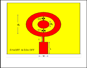
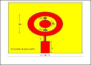
The conventional circular patch structure was modified by introducing a circular slot that is shown in the Fig. 1. The inner diameter and outer diameter of circular slot are 2 mm and 4 mm respectively is inserted in the circular patch structure. The two diodes D1 and D2 are placed between the inner and outer circles in the circular slot configuration.
4 SIMULATED STRUCTURES AND RESULTS
The electromagnetic (EM) simulation software is used to simu- late the proposed structure of frequency reconfigurable mi- crostrip patch antenna. The structure of antenna is designed on substrate FR-4 with dielectric constant 4.54 and thickness is
1.6 mm. The frequency reconfigurations were achieved for three different cases as follows; Case-I: when both diodes are in off-state, Case-II: when one diode is in on-state and other diode in off-state, and Case-III: when both diodes are in on- state.
4.1 Case-I when both diodes (D1and D2) are in off-state
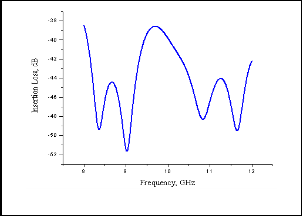
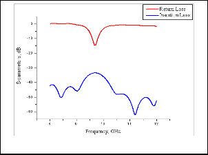
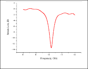
When both two diodes (D1 and D2) are in off-state then the two contacts is acting as open switch, so the result depends only on the circular configuration, the simulated return loss is at the frequency 9.69 GHz. The simulated design for case-I is shown in fig. 1. Diode D1 & D2 both are in off-state so the both diodes are works as open circuits. The simulated return loss for this structure is shown in fig. 2; the loss is -14.84 dB at the resonance frequency 9.69 GHz. The insertion loss of structure is shown in fig. 3. Comparison of reurn and insertion loss is shown in fig. 4.
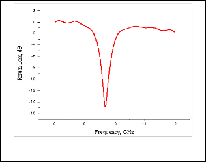
Fig.1. Reconfigurable design of circular patch antenna
3 RECONFIGURATION PROCEDURE
The circular patch antenna used in design is very easy to re- configure by connecting diodes between inner and outer circu- lar slots. There are three different configurations of the two connecting diodes (D1 & D2). In the first case, both two diodes (D1 and D2) are in off-state. Therefore, the inner slot is work as a single cavity resonator. In the second case, one diode (D1) is in on-state and it performs as a closed switch and another diode (D2) in off-state and it act as open switch. In third case, both diodes (D1 & D2) are in on-state and operate as the closed switches. Hence, the same structure can be reconfigur- ing for different cavities and it resonates on three different frequencies.
In the fabricated structure the diodes are replaced by using simply microstrip lines, because we know that in ideal case the diode works as an open switch for the off-state and works as a closed switch in on-state. Accordingly, in fabricated structures for the on-state of diodes are replaced by microstrip lines be- tween connectors and for off-state none any microstrip line is connected.
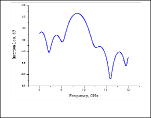
Fig.2. Simulated return loss for case-I
Fig.3. Simulated insertion loss for case-I
IJSER © 2012
http://www.ijser.org
International Journal of Scientific & Engineering Research, Volume 3, Issue 11, November-2012 3
ISSN 2229-5518
Fig.4. Comparison of return and insertion loss for case-I
Fig.7. Simulated insertion loss for case-II
4.2 Case-II when one diode (D1) is in on-state
When diode (D1) is in on-state then one contact is act as closed switch and another diode (D2) in off-state and it act as open switch, so result depends on the circular slot configuration and switchable configuration of diode D1. The simulated de- sign for case-II is shown in fig. 5. Diode D1 is in on-state and diode D2 is in off-state so one switch is works as closed switch and second works as open switch. As shown in fig. 6, the sim- ulated return loss is -11.87 dB at the resonance frequency 9.83
GHz, so now we can say that when diode D1 is on the reso-
nance frequency is shifted. The simulated insertion loss is
shown in fig. 7. Comparison of reurn and insertion loss is
shown in fig. 8.
Fig.8. Comparison of return and insertion loss for case-II
4.3 Case-III when both diodes (D1 & D2) are in on- state When both diodes are in on-state then both contects are act as closed switch, result depends on the circular slot configuration and switchable configuration of diodes D1 & D2. The simulat- ed design for case-III is shown in fig. 9. Diode D1 and diode D2 both are in on-state so both switches are work as closed switch. As shown in fig. 10, the simulated return loss is -13.43 dB at the resonance frequency 10.18 GHz, so when both diode are in on-state again the resonance frequency is shifted, so this frequency shifting shown the frequency reconfiguration. The simulated insertion loss is shown in fig. 11. Comparison of reurn and insertion loss is shown in fig. 12.
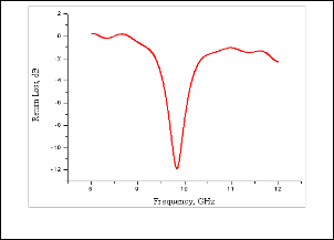
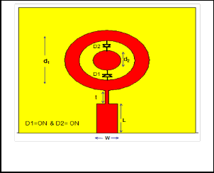
Fig.5. Simulated structure when diode (D1) is in on-state
Fig.6. Simulated return loss for case-II
IJSER © 2012
http://www.ijser.org
Fig.9. Simulated structure when diodes (D1 & D2) are in on-state
International Journal of Scientific & Engineering Research, Volume 3, Issue 11, November-2012 4
ISSN 2229-5518
The designed proposed structures were fabricated using the microwave integrated fabrication (MIC) technique (as mentioned in section 4.4.1) on the same substrate FR-4. The substrate has dimension 25.4 × 25.4 mm2, dielectric constant
4.54, and thickness 1.6 mm. The printed antennas were tested
using vector network analyzer (VNA). The measured results
are compared with simulated results for same three cases.
5.1 Case-I when both diodes (D1and D2) are in off-state
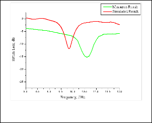
In fabricated structure for this case no any strip line in con- nected between the connectors as shown in fig. 13 and reso- nance frequency 10.33 GHz was measured for return loss be- low -10dB as shown in fig. 14. The comparison of measured and simulated return loss for case-I is shown in fig. 15.
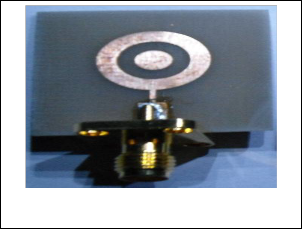
Fig.10. Simulated return loss for case-III
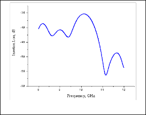
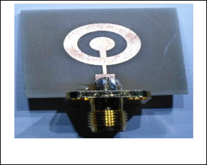
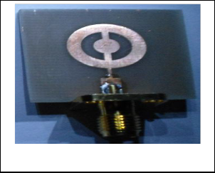
Fig.13. Fabricated structure when diodes (D1 & D2) are in off-state
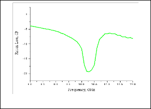
Fig.11. Simulated insertion losses for case-III
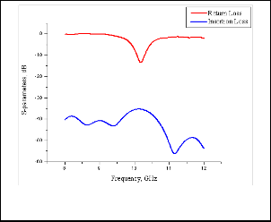
Fig.14. Measured return loss for case-I
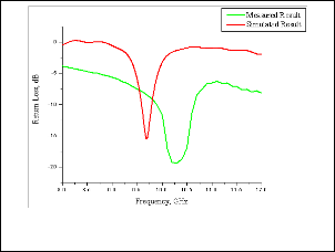
Fig.12. Comparison of return and insertion losses for case- III
5 FABRICATED STRUCTURES AND RESULTS
In the fabricated structure the diodes are replaced by using simply microstrip lines, because we know that in ideal case the diode works as an open switch for the off-state and works as a closed switch in on-state. Accordingly, in fabricated struc- tures for the on-state of diodes are replaced by microstrip lines between connectors and for off-state none any microstrip line is connected.
IJSER © 2012
http://www.ijser.org
Fig.15. Comparison of measured and simulated return loss for case-I
International Journal of Scientific & Engineering Research, Volume 3, Issue 11, November-2012 5
ISSN 2229-5518
5.2 Case-II when one diode (D1) is in on-state
In fabricated structure for this case diode D1 is replaced by connecting strip line between the connectors of diode D1 as shown in fig. 16 and return loss below -10dB on the resonance frequency 10.59 GHz as shown in fig. 17. The comparison of measured and simulated return loss for case-II is shown in fig.
18.
5.3 Case-III when both diodes (D1 & D2) are in on- state
In fabricated structure for this case diode D1 and Diode D2 are replaced by connecting strip lines between the connectors of diode D1 and diode D2 as shown in fig. 19 and the resonance frequency 11.01 GHz at the return loss below -10 dB as shown in fig. 20. The comparison of measured and simulated return loss for case-III is shown in fig. 21.
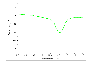
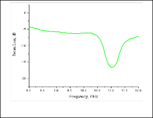
Fig.16. Fabricated structure when one diode (D1) is in on- state
Fig.19. Fabricated structure when diodes (D1 & D2) are in on-state
Fig.17. Measured return loss for case-II
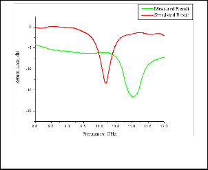
Fig.20. Measured return loss for case-III
Fig.18. Comparison of measured and simulated return loss for case-II
Fig.21. Comparison of measured and simulated return loss for case-III
IJSER © 2012
http://www.ijser.org
International Journal of Scientific & Engineering Research, Volume 3, Issue 11, November-2012 6
ISSN 2229-5518
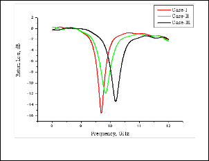
6 COMPARISON OF RESULTS
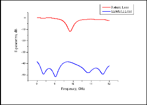
By comparing the return loss; S11 parameters for these three cases we can easily judge the effect of different diode connec- tion configurations and also the change in bandwidth and res- onance frequency as shown in fig. 22. The number of tuning frequencies is shifted as the numbers of ON-state diodes are increased in the structure.
.
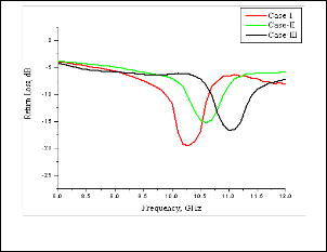
Fig.22. Comparison of simulated return losses
Fig.23. Comparison of measured return losses
The measured results for frequency reconfigurable antenna are shown in the fig. 23. The measured results are showing the close agreement with the simulated results. The proposed an- tenna can be used in the wireless communication
7 CONCLUSION
In this paper, the design of a reconfigurable circular microstrip patch antenna has been described and their simulated results are compared with measured results. This reconfigurable patch antenna can be used for different resonance frequencies. By analyzing simulated and measured results, it showed that by using circular slot and diode switching the return loss shifts and hence the resonance frequency is also changed. This reconfigurable antenna can further be modified by using RF- MEMS switches for fast switching purposes.
REFERENCES
[1] D. Schaubet. “Frequency-Agile Polarization Diverse Microstrip An- tennas and Frequency Scanned Arrays [P]”, US Patent #4, 367, 474, Jan. 4, 1983.
[2] Denidni, T.A., Lee, L., Lim, Y., and Rao, Q., “Wide-band high- efficiency printed loop antenna design for wireless communication systems”, IEEE Trans. Veh. Technol., 2005, 54, (3), pp. 873–878.
[3] Wong, T.P., and Luk, K.M, “A wide bandwidth and wide beamwidth CDMA/GSM base station antenna array with low backlobe radia- tion”, IEEE Trans. Veh. Technol., 2005, 54, (3), pp. 903–909.
[4] Xiao, S.Q., Shao, Z.H., Fujise, M., and Wang, B.-Z., “Pattern reconfig- urable leaky-wave antenna design by FDTD method and Floquet’s theorem”, IEEE Trans. Antennas Propag. 2005, 53, (5), pp. 1845–1848.
[5] Yang, F., and Rahmat-Samii, Y, “Patch antennas with switchable slots (PASS) in wireless commu- nications: concepts, designs, and applica- tions”, IEEE Antennas Propag. Mag., 2005, 47, (2), pp. 13–29.
[6] Peroulis, D., Sarabi, K., and Katehi, L.P.B., “Design of reconfigurable
slot antennas”, IEEE Trans. Antennas Propag. 2005, 53, (2), pp. 645–
654.
[7] Freeman, J.L., Lamberty, B.J., and Rews, G.S., “Optoelectronically
reconfigurable monopole antenna”, Electron. Lett. 1992, 28, (16), pp.
1502–1503.
[8] Z. Jiajie, W. Anguo, and W. Peng, "A Survey on Reconfigurable
Antennas”, Int. Con! Microwave Millimeter Wave Tech. Proc., vol. 3, Apr.
2008, pp. 1156-1159.
[9] M.Y. Ismail, M. Inam and J.Abdullah, “Design Optimization of Recon- figurable Reflectarray Antenna Based on Phase Agility Technique”, Conference on Antennas, Propagation and Systems (INAS 2009), Dec.2009.
[10] C.A.Balanis, “Antenna Theory, Analysis and Design”, John Wiley &
Sons, New York, 1997.
[11] M.-I. Lai, T.-Y. Wu, J.-C. Hsieh, C.-H. Wang, and S.-K. Jeng “Design of reconfigurable antennas based on an L-shaped slot and PIN diodes for compact Wireless devices”, IET Microwave. Antennas Propag. 2009, Vol. 3, Iss. 1, pp. 47–54.
[12] G. Monti, L. Corchia, and L. Tarricone, “Patch Antenna with Recon-
figurable Polarization”, Progress In Electromagnetics Research C, Vol. 9,
13-23, 2009.
[13] G. Singh, M. Kumar “Design of frequency reconfigurable Microstrip patch antenna”, 6th IEEE International Conference on Industrial and Infor- mation Systems, ICIIS, Aug. 2011, pp. 18-22.
[14] G. Singh, M. Kumar “Novel Frequency Reconfigurable Microstrip Patch Antenna Based on a Square Slot for Wireless Applications”, IEEE International Conference on Communication System and Network Technolo- gies (CSNT), May-2012, pp. 27-30.
IJSER © 2012
http://www.ijser.org