International Journal of Scientific & Engineering Research, Volume 4, Issue 4, April-2013 473
ISSN 2229-5518
Flyback with Half Wave Rectifier for Single Stage Power Factor Correction K.Umamaheswari*, V.Venkatachalam **
* Research Scholar, Anna University, Chennai.
** Principal, The Kavery Engineering College, Mecheri.
Abstract - The flyback converter type single-stage converter and a half wave rectifier with time-multiplexing control (TMC) for power factor correction is proposed. It has the advantage of better magnetic core utilization and better performance for high power applications. The major portion of the input is transferred to the load through ac-dc conversion. And the part of the input power is delivered to the auxiliary output through the flyback conversion and stored in the capacitor. The voltage ripple of the main output can also be reduced. With TMC the power processes can be achieved by single transformer to reduce the cost and the size of the converter. The simulation result of the proposed converter presents, simplicity, high power factor with low cost and size.
Index Terms -Power Factor Correction (PFC), Single –Stage, Flyback Converter.
1. INTRODUCTION
During the past two decades, power electronics research has focused on the development of new families of hard- and soft-switching converter topologies used in the design of dc–dc and ac–dc converters with active power factor corrections (PFC’s). The goal is to design high- efficiency and high-power density converters with improved power factor and low electromagnetic interference (EMI). In recent years, as the new standards such as IEC 1000-3-2 became compulsory regarding limiting the total harmonic distortion (THD) and input power factor in power electronic circuits, researchers are actively seeking ways to shape the line current waveform to achieve THD and power factor that comply with international standards. Active PFC circuits that use pulse width modulation (PWM) switch-mode topologies such as the boost, buck–boost, and their derived ones have been used dominantly.
The steady-state analyses for a large number of such topologies are well documented, and their various dc control characteristics are well known. In addition to the steady-state behavior, the dynamic behavior is equally important and critical when it comes to the design of a robust control system for such converters. Control theory is applied to improve the performance of power electronics circuits such as the transient response, control accuracy, regulation capability and to reduce the effects of parameter variations as well as other disturbances. Over the last two decades, several control schemes have been presenting various modeling techniques for the power stage. A novel one-switch one-stage converter is proposed in, which features universal line voltage operation, near unity power factor, high efficiency, and low THD in the input current.
With the increasing demand for power from the ac line and more stringent limits for power quality, power factor correction has gained great attention in recent years
Power Factor Correction (PFC) technique continues to be attractive research topic with several effective regulations being reported. Conventional cascade of two stage topology can achieve good performance such as high power factor and low voltage stress, but it usually suffers from high cost and increased circuit complexity. Many single-stage PFC AC/DC converters have been proposed that can be applied cost-effectively. However, it’s well known that in single stage topologies, the voltage across the bulk capacitor can not be controlled well due to the fact that only one switch and control loop are used. Moreover, the storage capacitor voltage varies widely with the input voltage and load variation, especially when the PFC operates in DCM mode while DC/DC stage operates in CCM mode. Finally, the storage capacitor voltage will increase to be unbearable under light load condition.
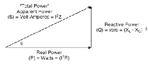
Fig.1 Power Factor Triangle (Lagging)
Power Factor Correction (PFC) converter is necessary for many electronic types of equipment to meet harmonic regulations and standards, such as IEC 1000-3-2. For low power applications, single-stage PFC converter is a better choice considering cost and performance. In single switch topologies, a PFC cell is integrated with a DC/DC
IJSER © 2013
http://www.ijser.org
International Journal of Scientific & Engineering Research, Volume 4, Issue 4, April-2013 474
ISSN 2229-5518
conversion cell and both cells share active switches and controller. But those topologies suffer from high voltage
and high current stresses. But most of those methods will bring high distortion to line current waveform, resulting in reduced power factor. In recent years the power factor correction problem is solved by single-stage flyback converter with time multiplexing control [1].
In order to improve the power factor, several single stage PFC circuits have been developed. Flyback and forward converters are the common topologies for active PFC [2], [5],[15],[16].These converters allow the input current to be shaped into a rectified sine wave, which is in phase with the input voltage, achieving the high power factor. Resonant power factor correction circuits have been introduced which are named as full-bridge and half-bridge [17], [18]. Soft switching technique has also been used in these converters [7], [8], [13], [17]. The single stage soft switching regulators are attractive because of its soft commutation and low voltage stress. Single-stage parallel PFC schemes or direct power transfer (DPT) technique is also used. Fig.2. There are several disadvantages of the two- stage PFC converter, for example, the total efficiency of the two-stage is lower because the total power has to be processed twice with two cascade power stages and each power stage has to be rated as full output power which will increase the size and cost of the circuits.
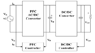
Fig. 2 Two-stage Power-Factor-Corrected (PFC) Converter approach
The proposed converter in this paper consists of a forward converter integrated with an auxiliary flyback converter. The major input power is delivered directly to the load through the forward converter avoiding double power processing while excessive energy is stored in the capacitor of the auxiliary flyback converter. The overall efficiency of the system can be improved by maximizing the power processed by the forward converter. The line- frequency voltage ripple of the main output is minimized by controlling the energy transferred from the auxiliary
output to the main output by applying the time multiplexing control (TMC). TMC has been introduced in
telecommunication systems. The channel divides into N time slots and transmits each signal through the assigned time slot. This solves the problem when the resource is limited. This paper applies TMC technique to controlling the auxiliary output. This output has its own feedback control circuit to control switch to regulate the output voltage and to minimize the output ripple.
PFC converter proposed in consists of a single forward converter operating in discontinuous conduction mode (DCM). In order to reduce the low frequency output voltage ripple, an auxiliary circuit with a bulk capacitor is used to produce an anti-phase voltage ripple to the line frequency ripple. However, there is no isolation between the bulk capacitor and the output. The high bulk capacitor voltage would cause safety issues.
2. TOPOLOGY AND OPERATION PRINCIPLE
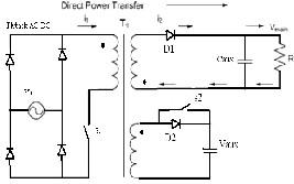
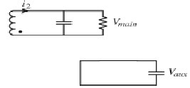
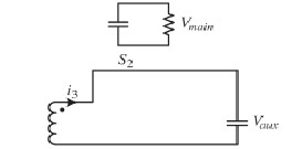
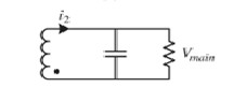
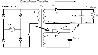
Fig. 3 shows the topology of the proposed single-stage PFC circuit based on a forward AD/DC converter. The circuit consists of a forward converter with an auxiliary circuit with a transformer T1, a reset winding L3, a capacitor Caux, a diode D3, and a switch S2. With the control of S1, the major power is directly transferred through the forward part to the load. The output voltage is represented by Vmain. Some energy is transferred to the auxiliary circuit, stored in Caux. With the control of S2, the power is transferred from auxiliary flyback part to the main output. Low output line-frequency voltage ripple is obtained by controlling the power from the auxiliary circuit through the duty cycle of S2.The signal of switches S1 and S2 are shown in Fig, 3. With the TMC control, switch S1 operates during t0-t1 period while S2 operates during t2-t3 period. The operation of current can be divided into five stages.
Fig. 3 Flyback converter and half wave rectifier
IJSER © 2013
http://www.ijser.org
International Journal of Scientific & Engineering Research, Volume 4, Issue 4, April-2013 475
ISSN 2229-5518
inductance. This keeps input current to flow into the circuit, preventing any dead angle of input current to occur. The load at main output is supplied by the capacitor Cmain.
a) Stage I
(b) Stage II
(c) Stage III
(d) Stage IV
Fig.4 Equivalent circuit of each stage
Stage II
The switch turns off and switch S2 is off in this stage.
The energy previously stored in the magnetic field is
delivered to the main output through flyback conversion. At the same time, the free-wheeling diode in the auxiliary out is on.
Stage III
The switch S2 turns on and switch S1 is off in this stage. The auxiliary output capacitor stores energy in the transformer through the auxiliary winding. The load at main output is supplied by the capacitor Cmain.
Stage IV
The switch S2 turns off and switch S1 is off in this
stage. The energy is thus transferred from the auxiliary output to the main output through the flyback conversion in Stage III. The main output voltage can be well regulated by controlling the turn-on time of the switch S2.
3. CIRCUIT ANANLYSIS AND DESIGN CONSIDERATION
a) Conventional two stage PFC
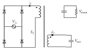
Stage I
The switch S1 turns on and switch S2 is off in this
stage. The supply voltage |Vin| charges the primary
inductance. Meanwhile, the supply voltage transfers power to the auxiliary output through forward conversion when
|Vin| is larger than the reflected voltage from the auxiliary voltage Vaux. Otherwise, the transformer acts solely as a coupled inductor, storing energy through the primary
IJSER © 2013
http://www.ijser.org
b) Proposed single-stage PFC scheme
Fig. 5 Power transfer diagrams
International Journal of Scientific & Engineering Research, Volume 4, Issue 4, April-2013 476
ISSN 2229-5518
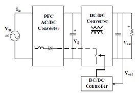
For not only the two-stage PFC converter scheme but
also the single-stage PFC converter shown in Fig. 5, the input power had to transferred twice before producing to the load. The input power is firstly transferred to store in the bulk capacitor though the PFC AC/DC stage. Then, it is transferred to the load through the DC/DC stage. These result that the overall efficiency is reduced due to the double power transferred. The proposed PFC converter applies direct power transfer (DPT) to increase the overall power conversion efficiency. Part of the input power P1 is directly transferred to the output, rest of the power P2 is delivered to the auxiliary output and stored in the bulk capacitor with some losses.
Efficiency
For both the conventional two-stage PFC scheme and
the single-stage PFC scheme sharing one power switch, the input power have been processed twice before applying to the load, the input power is first transferred through PFC functional stage to store in intermediate bulk capacitor. The stored power is then transferred through dc–dc functional stage to the load. Double power processing results in low overall efficiency of those schemes.

P =η1 . k .Pin
P2 =η2 .(1- k) .Pin
P3 =η . P2

Pout =P1 + P 2
where

= efficiency of the flyback ac-dc stage(P1)

2 = efficiency of the half wave rectifier ac-dc stage (P2)
3 = efficiency of the flyback ac-dc stage(P3)
k= percentage of input power directly transferred to the load
The proposed single-stage PFC scheme uses DPT idea to achieve high overall efficiency. The part of the input power P1 is directly transferred to the output and rest of input the power P2 is delivered to the auxiliary output and stored in the intermediate bulk capacitor (auxiliary). Eventually, the stored power P3 will be transferred to the main output through flyback dc–dc conversion with TMC.
This topology has been simplified with fewer components to save cost.The auxiliary output voltage is still naturally clamped within the range.The bulk capacitor (auxiliary)is charged directly when the switch S1 turns on; it results in high initial input current i1 which is reflected from the auxiliary output current i3.
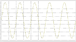
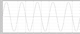
(a) With 220V input voltage

(b) Input current

(c) Input pulse to the switches
IJSER © 2013
http://www.ijser.org
International Journal of Scientific & Engineering Research, Volume 4, Issue 4, April-2013 477
ISSN 2229-5518
obtained according to maximize the percentage of DPT. Only a single transformer is used for all the power conversion. The simulation results confirm the effectiveness of the proposed scheme for the proposed Single-Stage PFC converter.
(d) Waveform of line voltage and line current
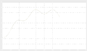
(e) Output DC voltage waveform
Fig.6 waveforms of input voltage, line current, output
voltage and input pulses
The input voltage Vin and input current Iine are shown in Fig.6. It indicates that high power factor has been obtained with the proposed PFC converter by applying the different input voltages. The input current is nearly perfect sine wave. The reason causing this result is when Vin is larger than the Vmain, the major input power transfer to the output through the forward conversion; when Vin is smaller than the Vmain, the circuit is worked as a flyback converter. This avoids the dead-angle appeared, increases the power factor compared to a classical forward converter. The third harmonic in the input is largely caused by the zero-crossing distortion.THD is 3.91% when upto 40th harmonic are measured. The zero-crossing distortion energy is spread among multiple frequencies at 5th, 7th, 9th and 11th harmonics, such that THD is actually lower than that under 60Hz input.
4. CONCLUSION
The replacement of forward converter by the half wave rectifier gives the cost efficiency and high power factor. A forward-based Single-Stage PFC converter with TMC based on direct power transfer (DPT) concept is proposed in this paper. High power factor is achieved which is shown in the simulation result. Successful control of TMC of the auxiliary power switch results in lower output voltage ripple and tight voltage regulation. High efficiency is
REFERENCES
[1] “Flyback-Based Single-Stage Power-Factor-Correction Scheme With Time-Multiplexing Control Jun Zhang, Dylan Dah-Chuan Lu, Senior Member, IEEE, and Ting Sun-IEEE transaction vol-57,no:3,march-2010.
[2] M.A.Dalla Costa, J.M.Alonso, J.C.Miranda, and
D.G.Lamar,“A single-stage high-power-factor
electronic ballast based on integrated buck flyback converter to supply metal halide lamps,” IEEE Trans.Ind.Electron.,vol.55,no.3,pp.1112– 1122,Mar.2008.
[3] M.G.Egan, D.L.O’Sullivan, J.G.Hayes, M.J.Willers, and
C.P.Henze,“Power-factor-corrected single-stage
inductive charger for electric vehicle batteries,” IEEE
Trans. Ind. Electron. ,vol.54,no.2, pp.1217–
1226,Apr.2007.
[4] G.Moschopoulos and P.Jain,“ Single-phase single-stage
power-factor Corrected converter topologies,” IEEE
Trans. Ind. Electron., vol.52, no.1, pp .23–35 ,Feb.2005.
[5] H.F.Liu and L.K.Chang, “Flexible and low cost design
for a flyback AC/DC converter with harmonic current correction,” IEEE Trans .Power Electron. , vol.20, no.1, pp.17–24, Jan.2005.
[6] J.M.Kwon, W.Y.Choi, and B.H.Kwon, “Single-switch
quasi-resonant converter,” IEEE Trans. Ind. Electron.,
vol.56, no.4, pp.1158–1163, Apr.2009.
[7] E.Adib and H.Farzanehfard, “Family of zero-current
transition PWM converters,” IEEE Trans .Ind.
Electron., vol.55, no.8, pp.3055–3063, Aug.2008.
[8] Y.M.Liu and L.K.Chang,“Single-stage soft-switching
AC–DC converter with input current shaping for universal line applications,” IEEE Trans. and.Electron., vol.56, no.2, pp.467–479, Feb.2009.
[9] L.Antonio, B.Andrs, S.Marina, S.Vicente, and O.Emilio,
“New power factor correction AC–DC converter with
reduced storage capacitor voltage,” IEEE Trans.
Ind.Electron.,vol.54, no.1, pp.384–397,Feb.2007.
[10] R. Redl, L. Balogh, and N. O. Sokal, “A new family of single-stage isolated power-factor correctors with fast regulation of the output voltage,” in Proc. 25th Annu EEE PESC, Jun. 1994, vol. 2, pp. 1137–1144.
[11] C. M. Wang, “A novel single-switch single-stage
electronic ballast with high input power factor,” IEEE Trans. Power Electron., vol. 22, no. 3, pp. 797–803, May
2007.
[12] M. Ponce, A. J. Martinez, J. Correa, M. Cotorogea, and
J. Arau, “Highefficient integrated electronic ballast for
IJSER © 2013
http://www.ijser.org
International Journal of Scientific & Engineering Research, Volume 4, Issue 4, April-2013 478
ISSN 2229-5518
compact fluorescent lamps,”IEEE Trans. Power
Electron., vol. 21, no. 2, pp. 532–542, Mar. 2006.
[13] C. S.Moo, K. H. Lee, H. L. Cheng, and W.M. Chen, “A single-stage high power-factor electronic ballast with ZVS buck-boost conversion,” IEEE Trans. Ind. Electron., vol. 56, no. 4, pp. 1136–1146, Apr. 2009.
[14] J. Y. Lee and M. J. Youn, “A single-stage power-factor-
correction converter with simple link voltage suppressing circuit (LVSC),” IEEE Trans. Ind. Electron., vol. 48, no. 3, pp. 572–584, Jun. 2001.
[15] J.J.Lee, J. M. Kwon, E. H. Kim, W. Y. Choi, and B. H.
Kwon, “Single stage single-switch PFC flyback
converter using a synchronous rectifier,” IEEE Trans. Ind Electron., vol. 55, no. 3, pp. 1352–1365, Mar. 2008.
[16] K.Feel-Soon, P. Sung-Jun, and U. K. Cheul, “ZVZCS single- stage PFC AC-to-DC half-bridge converter,”IEEE Trans. Ind. Electron., vol. 49,no. 1, pp.
206–216, Feb. 2002.
[17] S. Kyoung - Wook and K. Bong-Hwan, “A novel single-
stage half- bridge AC–DC converter with high power
factor,” IEEE Trans. Ind. Electron.,vol. 48, no. 6, pp1219–
1225, Dec. 2001.
[18] D. Dai, S. N. Li, X. K. Ma, and C. K. Tse. "Slow-Scale Instability of Single-Stage Power-Factor-Correction Power Supplies." IEEE Trans. On Circuits and Systems I: Regular Papers, vol.54, pp.1724-1735, Aug
2007.
[19] B. R. Lin, C. L. Huang, and M. Y. Li. "Novel zero voltage switching dual-switch forward converter with
ripple current cancellation." Electric Power Applications, IET, vol.1, pp.799-807, Sep 2007.
[20] R. T. Chen and Y. Y. Chen, “Single-stage push–pull boost converter with integrated magnetics and input current shaping technique,” IEEE Trans.Power Electron., vol. 21, no. 5, pp. 1193–1203, Sep. 2006.
[21] A. Fernandez, J. Sebastian, F. F. Linera, and A. Ferreres,
“Single-stage AC-to-DC converter with self-driven synchronous rectification that complies with EN61000-
3-2 regulations,” IEEE Trans. Ind. Electron., vol. 50,no. 5,
pp. 1062–1064, Oct. 2003.
[22] J. A. Villarejo, J. Sebastian, F. Soto, and E. de Jodar,
“Optimizing the design of single-stage power-factor
correctors,” IEEE Trans. Ind. Electron.,vol. 54, no. 3, pp.
1472–1482, Jun. 2007.
[23] J. Y. Lee, “Single-stage AC/DC converter with input- current dead-zone control for wide input voltage ranges,” IEEE Trans. Ind. Electron., vol. 54, no. 2, pp.
724–732, Apr. 2007.
[24] A. K. S. Bhat and R. Venkatraman, “A soft-switched
full-bridge singlestage AC-to-DC converter with low- line-current harmonic distortion,” IEEE Trans. Ind. Electron., vol. 52, no. 4, pp. 1109–1116, Aug. 2005..
IJSER © 2013
http://www.ijser.org