.
International Journal of Scientific & Engineering Research, Volume 5, Issue 12, December-2014 1361
ISSN 2229-5518
FPGA Implementation Of Irrigation Control
System
K.Sindhu1, Y.Sri chakrapani2, M. Kamaraju3
Abstract— The paper FPGA implementation of irrigation control system is mainly focused on controlling the irrigation system at the same time it will care the crop in all aspects for the benefit of agricultural system and provides sufficient irrigation in particular field. It consists of different sensors that are interfaced with FPGA. The sensors will monitor the field conditions, and the sensors information will be stored in memory. Here the farmer will take the required information and he can take necessary precautions to his fields. The parameters for different devices were compared. By using HDL language the overall system architecture was designed. The simulation and synthesis are done using EDA tools.
Index Terms— Field Programmable Gate Array (FPGA), Flash memory, Sensors, EDA tools, HDL
—————————— ——————————
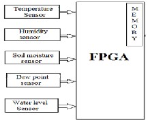
This system will monitor all these parameters through differ- ent sensors. Soil moisture sensor will measure the water con- tent in the soil i.e.; it will check whether the soil is dry or wet. Water level sensor senses the water in the water source. Tem- perature sensor and humidity sensor are used for forecasting the weather conditions. Dew point sensor will convert the wa- ter vapor into liquid state.
.
Fig. 1 system architecture of irrigation control system
When any of the climatic parameters like temperature, humid- ity, water level, soil moisture and dew point etc. cross a safety threshold which has to be maintained to protect the crops the sensor sense the change and the FPGA reads this data at its input ports after being converted to a digital form by the ADC
.The FPGA then performs the needed actions. As the system also employs memory in which all the sensor values are stored.
A temperature sensor is used to measure the temperature of the fields. This is most effective field parameter which has greater influence on other parameters.
Humidity is the presence of water in air. In agriculture, measurement of humidity is important for plantation protection and soil moisture monitoring. The humidity sensor is also called a hygrometer. It continuously measures and re- ports the relative humidity in the air.
The humidity sensor senses relative humidity. That means it measures both air temperature and moisture. Relative humidity is expressed as a percentage. It is the ratio of actual moisture in the air to the highest amount of moisture air at that temperature can hold. The warmer the air is, the more
IJSER © 2014 http://www.ijser.org
International Journal of Scientific & Engineering Research, Volume 5, Issue 12, December-2014 1362
ISSN 2229-5518
moisture it can hold, so relative humidity changes with fluctu- ations in temperature.
Dew point temperature is measured in (°C or °F). Dew point is the temperature where condensation begins, or where the rela- tive humidity would be 100% if the air was cooled.
Soil moisture sensor measures the water content in soil. Meas- uring soil moisture is very important in agriculture to help farmers manage their irrigation systems more efficiently. Farmers able to generally use less water to grow a crop, they are able to increase yields and the quality of the crop by better management of soil moisture during critical plant growth stages.
The virtex 6 FPGA has less delay when comparing with other FPGA devices like Spartan 3E, virtex 4and virtex 5.Virtex 6 is more efficient. The main features of this FPGA is it has a 12 bit
1Msbs analog to digital convertor inbuilt XADC, having 16 external user configurable analog input channels. And by us- ing this we can connect 16 analog sensors at a time and store all parameter values in a PROM memory.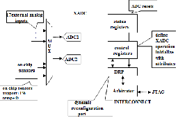
Fig. 2 XADC overview
The XADC contains dual 12 bit 1Mpbs analog to digital con- verter. It has 17 analog user configurable inputs. It has on chip thermal and supply sensors. .it is having a track and hold am- plifiers, which will supports a range of analog input signal types, which includes unipolar, bipolar, and differential. These analog inputs will support the signal bandwidth of atleast 500 kHz at the sample rates of 1Msbs. It has the basic on chip and power supply rails
Agriculture sensors which are used to analyze different field parameters are interconnected to a 6- series FPGA kit which contains 17 external analog input pins. Mostly 16 sensors are connected at a time by using the above kit. By changing this analog results into digital and obtain the re- lated field parameter values and get this value at the end of FPGA core in 6 series FPGA kit. Then we can store this val- ues in ROM memory by using FPGA to prom memory in-
terconnect. We can store all these results in the external
ROM memory.
In agriculture there exist different threshold limits to all
parameters like temperature, Humidity, dew point, water
level and soil moisture etc. If the values stored in the regis-
ters of the FPGA board crosses the threshold limits then all
the field parameters values will be stored in memory.
The field-programmable gate arrays (FPGA) has on chip memory. It has the routing structure between the memory ar- rays and logic resources. For the maximum flexibility and bet- ter performance, a PROM flash memory is connected external- ly to the FPGA, which is used for storing the data. The flash memory is used for storing the various samples which are coming out from LASER beam through ADC. From the flash memory we can compare different multiple samples and the required data will be passes through DDS interface. The memory interface for an FPGA-based design have three fun- damental building blocks: the Read &Write and Data interface, the memory controller state machine, and the user interface that bridges the memory interface design to the rest of the FPGA design. The user sends a command read or writes along with the address and data for write, the Memory interface clocking requirements are typically more difficult to meet when reading from memory, as compared with writing to memory.
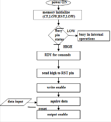
Fig.3 Flow chart for Flash Memory
When the power is ON, the FPGA will send low signal to the RST pin. When it was active the RST pin will set the device in to read array mode. And hence the data can be read by send- ing a high signal on RST pin and making CE-low, OE-low, WE-high, after completion of one cycle the FPGA reads the BUSY pin, a LOW on this pin indicates that it was performing some internal operations. And HIGH on this will indicates it was RDY to receive new commands. And similarly when the RST pin is HIGH we can WRITE the data.
IJSER © 2014 http://www.ijser.org
International Journal of Scientific & Engineering Research, Volume 5, Issue 12, December-2014 1363
ISSN 2229-5518
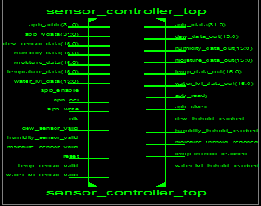
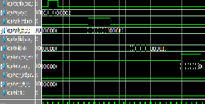
Fig 6: Simulation waveform for sensors
The above fig 6 shows the simulation waveform for the out- puts of the sensors. Here if the sensor crosses the threshold value that result will be displayed as its output.
Fig 4: RTL Schematic Diagram of sensor controller and memory
The above fig 4 shows the RTL schematic diagram of all the sensors and memory interface in which one can clearly observe the sensors inputs and outputs.for fpga temperature sensor data,soil moisture data,humidity data,dew sensor data were given as inputs to the fpga,moreover the memory signals like enable,select,write,read signals were given as input.whenever all the sensors crosses its threshold limit that
output will be given to the soil moisture data out,humidity data out,dew data out,water level data out,temperature data out signals respectively.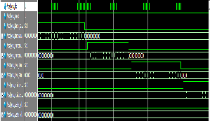
Fig 5: simulation waveform for all sensors
The above fig 5 shows the inputs that are given to the sen- sors. Here all the sensors will take the digital values as its in- puts, and it will check with the threshold limit whether it was crossing the limit or not.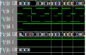
Fig 7: simulation waveform for memory
Fig 7 shows the simulation waveform for memory. Here whenever all the sensors cross its threshold value that information will be stored in memory
Table 1: Parameters Analysis Report
S.NO | DEVICES | DELAY(NS) | SLICE REG- ISTERS | LUTS |
1 | SPARTAN 3E | 10.98 | 277 | 267 |
2 | VIRTEX 4 | 8.411 | 277 | 267 |
3 | VIRTEX 5 | 5.931 | 310 | 180 |
4 | VIRTEX 6 | 3.209 | 310 | 180 |
Table 1 shows the comparison of different devices for parameters like delay, slice registers and LUTs. The delay is decreased when compared to Spartan 3E to vertex 6 as shown in table 1. By using vertex 6 the execution time is very less when compared to other devices
IJSER © 2014 http://www.ijser.org
International Journal of Scientific & Engineering Research, Volume 5, Issue 12, December-2014 1364
ISSN 2229-5518
FPGA implementation of irrigation control system leads to the improvement in yield of the crops. The system will monitor all the field parameters thus providing the necessary information to the farmers. It becomes very efficient to use in rural areas. The use of FPGA facilitates the system for re-configurability and re- programmability according to different environmental conditions. The usage of this FPGA enhances the application area of sensor networks in all agricultural environments by improving the speed of operation. In future these collected fields parameters data can be send to the farmer through wireless networks.
[1] Y. Kim, R. Evans and W. Iversen, “Remote Sensing and Control of an Irrigation System Using a Distributed Wireless Sensor Network”, IEEE Transactions on Instrumentation and Measurement, pp. 1379–
1387, July 2008.
[2] Xilinx -7 Series FPGAs Memory Interface Solutions Data Sheet
(v1.9).
[3] Xilinx 7-serise FPGA overview.
[4] Remote Monitoring in Agricultural Greenhouse Using Wireless Sen- sor and Short Message Service (SMS) International Journal of Engi- neering & Technology IJET-IJENS Vol:09 No:09.
[5] Remote Monitoring Using Wireless Cellular Networks International
Journal of Digital Information and Wireless Communications
(IJDIWC) 2(4): 79-83 The Society of Digital Information and Wireless
Communications, 2012 (ISSN: 2225-658X
• Ms.K.Sindhu is currently pursuing M.Tech in Embedded Systems Gudlavalleru Engineering College affiliated to JNTU, Kakinada, India. Email: Sindhu.akshaya777@gmail.com.
• Mr.Y.Sri Chakrapani is currently working as Associate professor in the Department of Electronics and Communications, Gud- lavalleru Egineering College, Gudlavalleru, India, Email id: srichakrapani@gmail.com.
• Mr.Dr. M. Kamaraju is currently working as Professor & Hod in the Department of Electronics and Communications, Gudlavalleru Egineering college, Gudlavalleru, India, Email id: mad- duraju@yahoo.com.
IJSER © 2014 http://www.ijser.org