International Journal of Scientific & Engineering Research, Volume 1, Issue 2, November-2010 1
ISSN 2229-5518
FPGA-Based Design of Controller for Sound Fetching from Codec Using Altera DE2 Board A.R.M. Khan, A.P.Thakare, S.M.Gulhane
ABSTRACT— The trend in hardware design is towards implementing a complet e system, intended for various applications, on a single chip. In order to implement the any speech application in Alt era DE2 board a controller is designed to control the CODEC and acquire the digital dat a from it. This paper presents an experimental design and implementation of the controller using the specification given by the Philips for I2C protocol & DSP mode of operation of CODEC on cyclone-II EP2C35F72C6 FPGA in Altera DE2 board . A controller was designed using VHDL language, which performs the two operations: I2C protocol operation to drive the W olfson Codec W M8731, sound fetching from W olfson Codec WM8731 to FPGA in DSP m ode. Altera Quartus II 9.0 sp2 web Edition is used for the synthesis of the VHDL logic on FPGA and ModelSim- Altera 6.5b (Quartus II 9.1) Starter Edition is used for the simulation of VHDL logic. Three modules have been created in the design: the I2C bus controller, virtual sound fetcher, and the clock module. The FPGA communicates with the W olfson via the I2C (Inter-Integrated Circuit) protocol using two pins: 'SDIN' (the data line), and 'SCLK' (the bus clock). I2C bus controller modifies internal settings of Codec, de-mute the microphone input, boost the microphone volume, and change the default sound path (so that the microphone is given priority over other inputs). After the codec digitalizes the input it put the digital data on digital audio interface, to fetch the data on DACDAT of codec form digital audio interface DSP mode of operation of codec is used in the design. DACDAT is the formatted digit al audio data stream with left and right channels multiplexed toget her. DACLRC (alignment clock) and BCLK (synchronization clock) is used to fetch the dat a on DACDAT this dat a can be use for any sound application. Clock module is design to generate different clock requirem ent for the controller.
Keywords— I2C bus controller, Quartus II, ModelSim, Codec, Virtual Sound fetcher.
—————————— • ——————————
provided with the DE2 board features the Quartus® II Web
I. INTRODUCTION
FPGA becomes one of the most successful of today’s technologies for developing the systems which require a real time operation. The term field Programmable highlights the customizing of the IC by the user, rather than by the foundry manufacturing the FPGA. Several researchers discussed the design of hardware systems. Numbers of these works were specialized in designing the controllers for different application, and were aim to get better control responses, FPGA are two dimensional arrays of logic blocks and flip-flops with an electrically programmable interconnection between logic blocks. The interconnections consist of electrically programmable switches which is why FPGA differs from Custom ICs, as Custom IC is programmed using integrated circuit fabrication technology to form metal interconnections between logic blocks. In an FPGA logic blocks are implemented using multiple level low fan in gates, which gives it a more compact design compared to an implementation with two-level AND-OR logic. FPGA provides its user a way to configure and these specifications. Altera DE2 board become one of the most widely development FPGA board which is used to development of FPGA design and implementations, the board offers a rich set of features that make it suitable for use in a laboratory environment for university and college courses, for a variety of design projects, as well as for the
development of sophisticated digital systems. Software
Edition CAD system, and the Nios® II Embedded Processor. Also included are several aids to help students and professionals experiment with features of the board, such as tutorials and example applications. Traditionally, manufacturers of educational FPGA boards have provided a variety of hardware features and software CAD tools needed to implement designs on these boards, but very little material has been offered that could be used directly for teaching purposes. Altera's DE2 board is a significant departure from this trend.
II. DE2 DEVELOPMENT BOARD
Altera DE2 board become one of the most widely development FPGA board which is used to development of FPGA design and implementations [5]. The purpose of the Altera DE2 Development and Education board is to provide the ideal vehicle for learning about digital logic, computer organization, and FPGAs. It uses the state-of the- art technology in both hardware and CAD tools to expose students and professionals to a wide range of topics. The board offers a rich set of features that make it suitable for use in a laboratory environment for university and college courses, for a variety of design projects, as well as for the development of sophisticated digital systems. Altera provides a suite of supporting materials for the DE2 board; including tutorials, “ready-to-teach” laboratory exercises, and illustrative demonstrations [6] Fig. 1 gives the block diagram of the DE2 board. To provide maximum flexibility
IJSER © 2010 http://www.ijser.org
International Journal of Scientific & Engineering Research, Volume 1, Issue 2, November-2010 2
ISSN 2229-5518
for the user, all connections are made through the Cyclone II FPGA device. Thus, the user can configure the FPGA to implement any system design.

Fig. 1: Block Diagram of DE2 Board [6]
III. STRUCTURE OF CONTROLLER
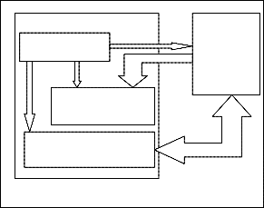
In order to implement the any speech application controller is design in the Altera DE2 board shown in the Fig. 2 the design is broken down into modules. These are then mapped to combinational logic and finite-state machines (FSM); using the Quartus II software package .Three modules have been created: I2C bus controller, Virtual sound fetcher, Clock module.
Cyclone-II EP2C35F72C6 FPGA
Wolfson Codec
Fig. 2: Block Diagram of controller
A. I2C bus controller
The FPGA communicates with the Wolfson via the I2C (Inter-Integrated Circuit) protocol using two pins: 'SDIN' (the data line), and 'SCLK' (the bus clock) Fig. 3 shows the complete requirement of data transmission through I2C .Within the procedure of the I2C bus, unique situations arise which are defined as START (S) and STOP (P) conditions. START means a HIGH to LOW transition on the SDIN line while SCLK is HIGH & STOP means a LOW to HIGH transition on the SDIN line while SCLK is HIGH .The master always generates START and STOP conditions. The bus is considered to be busy after the START condition. The bus is considered to be free again a certain time after the STOP condition. The bus stays busy if a repeated START (Sr) is generated instead of a STOP condition. In this respect, the START (S) and repeated START (Sr) conditions are functionally identical. The S symbol will be used as a generic term to represent both the START and repeated START conditions, unless Sr is particularly relevant. Detection of START and STOP conditions by devices connected to the bus is easy if they incorporate the necessary interfacing hardware. The content s of the data line are sent in the same order as seen in Fig. 3 (after a start condition): 'RADDR', 'R/W',
'ACK','DATAB[15-9]', and 'DATAB[8-0]', which stand respectively for “base address”, “Read/Write”, “acknowledge”, “control address”, and “control data”. The clock for the control serial data input is SCLK. The
maximum frequency for this signal is 400 kHz, the
Clock module
Virtual sound fetc her
I2C bus contr oller
DE2 Boa rd
WM8731
I2C bus
frequency used in this paper is f=50 MHz/128 = 390.625 kHz.
The data input signal is SDIN, it contains the information for the control interface [9]. The controller was reprogrammed using the 2-wire interface with the EP2C35F672C6 FPGA in Cyclone II board. After the start condition that is a falling edge on SDIN while SCLK is high. The following seven bits determines which device receives the data, the address depends on the CBS state (set to ground in this codec) so it is “0011010”. After this address, the bit R/W determines the direction of data transfer, in this case a ‘0’indicates ‘write’. The device recognizes the address and R/W by pulling SDIN low during the ninth clock cycle, acknowledging the data transfer. The control
follows with two bit blocks (separated with another
IJSER © 2010 http://www.ijser.org
International Journal of Scientific & Engineering Research, Volume 1, Issue 2, November-2010 3
ISSN 2229-5518
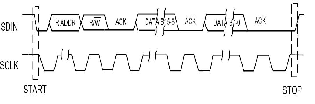
acknowledge) the first block B [15:9] contains the control address bits, and the second block B [8-0] contains the control data bits. The stop condition after the data transfer is a rising edge on SDIN when SCLK is high. If a start condition is detected out of the sequence at any point in the data transfer then the device will jump to the idle condition. After a complete control operation, the audio codec returns to the idle state and waits for another start condition.[9],[10]
Fig. 3: Requirement of data transmission through I2C
B. Virtual Sound fetcher
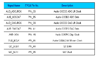
The WM8731 or WM8731L (WM8731/L) are low power stereo CODECs with an integrated headphone driver. The WM8731/L is designed specifically for portable MP3 audio and speech players and recorders. The WM8731 is also ideal for MD, CD-RW machines and DAT recorders. The on-board digital to analogue converter (DAC) accepts digital audio from the digital audio interface. Digital filter de-emphasis at 32 kHz, 44.1 kHz and 48 kHz can be applied to the digital data under software control. The DAC employs a high quality multi-bit high-order oversampling architecture to again deliver optimum performance with low power consumption. The DE2 board provides high-quality 24-bit audio via the Wolfson WM8731 audio CODEC (enCOder/DECoder). This chip supports microphone-in, line-in, and line-out ports, with a sample rate adjustable from 8 kHz to 96 kHz. The WM8731 is controlled by a serial I2C bus interface, this is connected to pins on the Cyclone II FPGA. A schematic diagram of the audio circuitry is shown in Fig. 4, and the FPGA pin assignments are listed in Table 1.[6],[7]
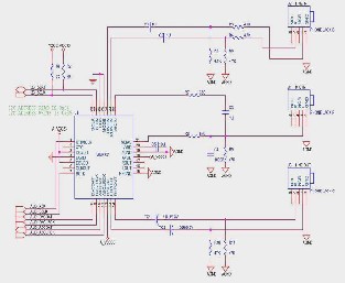
Fig. 4 Audio CODEC Schematic
TABLE.1
FPGA PIN ASSIGNMENTS
1) Slave Mode of Operation: As a slave device the WM8731/L sequences the data transfer (ADCDAT, DACDAT) over the digital audio interface in response to the external applied clocks (BCLK, ADCLRC, DACLRC). Note that the WM8731/L relies on controlled phase relationships between audio interface BCLK, DACLRC and the master MCLK.[8]
2) Digital Audio Interfaces: WM8731/L may be operated in either one of the 4 offered audio interface modes. All four of these modes are MSB first and operate with data 16 to 32 bits. These are:
• Right justified
• Left justified
IJSER © 2010 http://www.ijser.org
International Journal of Scientific & Engineering Research, Volume 1, Issue 2, November-2010 4
ISSN 2229-5518
• I2S
• DSP mode
3) Digital Audio Interface Formats in DSP Mode: There are four digital audio interface formats accommodated by the WM8731/L. DSP Mode format is shown in the Fig. 5 below. DSP mode is where the left channel MSB is available on either the 1st or 2nd rising edge of BCLK (selectable by LRP) following a LRC transition high. Right channel data immediately follows left channel data. To accommodate system timing requirements the interpretation of BCLK maybe inverted, this is controlled vias the software. This is especially appropriate for DSP mode.[8]
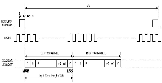
Fig. 5 DSP Mode format of CODEC
IV. DESIGNING OF CONTROLLER
A. I2C bus controller
For implementing the controller, finite-state machine (FSM) is used. However, even without any knowledge in digital logic design, you can still very easily implement a FSM by writing VHDL code. VHDL is popular hardware description languages (HDL) for designing digital circuits. A finite-state machine is a sequential circuit that uses a finite number of states to keep track of its history of operations, and based on this history and its current inputs, determine what to do next. The state variable declared using the SIGNAL keyword is the state memory. It is of type STD_LOGIC_VECTOR, which is an 8-bit bit string. The PROCESS block specifies that whenever there is a change in either of the two signals, clk and rst, the statements inside the block will be executed in sequential order starting with the first line. We have an active high reset signal as specified in the IF statement that tests for the
signal being a 1. When rst is deasserted, i.e., when rst is equal to 1, the module goes into the reset mode and outputs logic 1 value for both the SDIN and SCLK output signals. Furthermore, it assigns state x"00" as the initial state for when the FSM starts. x"00" is the syntax for the two hexadecimal digits 00. When rst is asserted, the ELSIF statement is executed.
The condition, Clock’ EVENT AND Clock = '1', specified
inside the ELSIF statement checks for a rising clock edge. So at every rising clock edge, the FSM will go to a new state and a new set of output signals will be generated [4] , To get 400kHz for I2C standard; every 2 cycles of 800kHz = 1
I2C cycle by using crystal frequency 50MHz/64 = 781kHz .
The clock for the control serial data input is SCLK maximum frequency for this signal is 400KHz that we are generating from 800KHz clock. The implementation of SDIN signal requires some special attention as it is bidirectional and open drain so to output the logic 1 on this line ,we need to set this to high impedance, to get high impedance we need to use tri-state output and assign to it a ’Z’ value. The condition signal assignment statement use in VHDL program is [1],[4]
SDIN <= ‘Z’ WHEN SDIN01 =’1’ ELSE ‘0’
B. Virtual Sound fetcher
Operating the digital audio interface in DSP mode allows ease of use for supporting the various sample rates and word lengths. The only requirement is that all data is transferred within the correct number of BCLK cycles to suit the chosen word length. In Slave mode, DACLRC and ADCLRC inputs are not required to have a 50:50 mark- space ratio. BCLK input need not be continuous.[8]
It is however required that there are sufficient BCLK cycles for each DACLRC/ADCLRC transition to clock the chosen data word length. The non-50:50 requirements on the LRCs is of use in some situations such as with a USB
12MHZ clock. Here simply dividing down a 12MHz clock
within the DSP to generate LRCs and BCLK will not generate the appropriate DACLRC or ADCLRC since they will no longer change on the falling edge of BCLK.[8]
For example, with 12MHz/32kfs mode there are 375
MCLK per LRC. In these situations DACLRC/ADCLRC can be made non 50:50. The 12MHz Clock is generated using
50MHz crystal oscillator available in DE2 board.
V. EXPERIMENTAL RESULTS
A. ModelSim- Altera 6.5b (Quartus II 9.1) (Results)
This is a program to simulate VHDL code. The VHDL
files are complied, the input signals are forced to the
IJSER © 2010 http://www.ijser.org
International Journal of Scientific & Engineering Research, Volume 1, Issue 2, November-2010 5
ISSN 2229-5518
correspondent values and the evolution of the signals is shown in waves and list. The simulation result of the I2C Controller with start & stop condition is shown in Fig. 7 and simulation result of the complete operation virtual sound fetcher is shown in Fig. 8
B. Quartus II (9.0)Sp2 Web Edition (Results) :
This is the main program and it is used to build the projects. It has many tools to prepare VHDL or VERILOG structures and download them to the board. The assignment of the pins is done with the Quartus II
Assignment Editor, after this the VHDL files can be
compiled and downloaded to the board with the
Programmer tool.[2]
In this project, JTAG programming ( Joint Test Action Group) is used so the configuration bit stream is downloaded directly into the FPGA that will retain the configuration as long as the power is applied to the board. Pin assignment used in the design is as shown Table.1 .You can view the internal structure of the design netlist technology map viewer. To view the post-fitting view of the schematic, you must first perform a full compilation, and then choose the, either after fitting or after Analysis & Synthesis, with the technology map viewer command.
To view the post-mapping view of the schematic, you must first perform Analysis & Synthesis, and then choose the technology map Viewer (Post-Mapping) command.
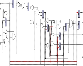
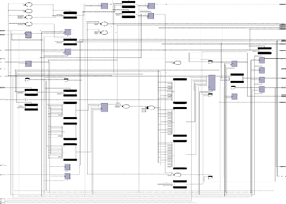
Synthesized design of the I2C Controller.(RTL view ) is as shown in Fig. 9 and synthesized design of virtual sound
fetcher is shown in Fig. 10 and Fig. 11 shows complete
Synthesized Design of virtual sound fetcher with I2C
specification (RTL view ).
C. Pin Assignment of FPGA
Quartus –II requires the pin assignment for the actual implementation of the design on FPGA in cyclone –II 475
I/O pins are available out of which 11 pin are used for the
port mapping in the design. Cyclone –II classify the pins into I/O bank and the assignment editor in Quartus –II provide the I/O standard general function and special function of the assign pin detail of Quartus-II window is as shown in the Fig. 6 .[11]
Fig. 6 FPGA Pin Mapping for the Design in Quartus-II
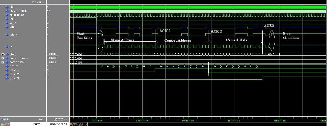
Fig. 7 Simulation result of the I2C Controller
IJSER © 2010 http://www.ijser.org
International Journal of Scientific & Engineering Research, Volume 1, Issue 2, November-2010 6
ISSN 2229-5518
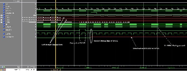
Fig. 8 Simulation result of the complete operation virtual sound fetcher
41 '' hh 00 ----

CIN
1
[4..0
B [4..0]
Less T han0
<
LESS_THAN
bcount~ [2..0]
SEL
3 ' h 7 -- DATAA
DATAB OUT
Mux13
SEL[ 7. .0]
2 41 ' h 1FFFFFFFFFFFFFFFFFFFFFFFFFFFFFFFFFFFFFFFFFFFFFFFFFFFFFFFEFFFE --
Mu x2
bcount[2..0]
Mu x4
SEL[7..0]
1 ' h 1 --
M ux5
SEL[ 7. .0]
clk
Bcount[1..0]
PRE
D Q
EN A
A[3..0 ]
1' h1--
B[3..0 ]
4'hD --
Add0
+
Bcount~[2..0]
SEL DATAA
OUT0
Bcount[2]
PRE
D Q
Equal 1
A [6..0]
Ad d1
M UX21
cl k_c ount800k[6..0]
DATA[25 5. .0]
OUT
CL K_8 0 0k _H z
PRE
D Q
D Q SEL[2..0]
8 ' h 0D -- D ATA[7..0] O UT
1' h1 - -
1' h1 - -
OUT
SDIN 01
PRE SDI N~ 0 co m b~0
D Q
1 ' h 0 --
1 ' h 0 --
OUT
s tat e[7 ..0 ]
PRE
D Q
Mu x3
SEL[7..0]
SCL K~ re g0
CLR
3' h4 - -
DATAB
A[2. 0].
B[2. 0]. =
BBcount~[13..7]
7' h01 --
B [6..0] +
ADDER
D Q
ENA
1' h1 --
ENA
CLR
ENA
Mu x1
M UX
1' h1 - -
D ATA[255..0]
0
ENA
CLR IO_BU F(TRI) BUF (DI REC T)
1 ' h 0 -- DATA[255..0]
25 6' hFFFFFFFFFFFFFFFFFFFFFFFFFFFFFFFFFFFFFFFFFFFFFFFFFFFFFFFFFFFF5 56 B--
3 ' h 0 --
DATA[25 5. .0]
OUT
D Q
ENA
SC LK
ADDER
ENA
3'h0--
7' h40 --
Less Than1
A [6..0]
B [6..0] <
LESS_THAN
7' h0 0 --
c lk_count800k~ [6. .0]
SEL DATAA
C LR
M UX
Mux14
SEL[ 7. .0]
8' h08 --
SEL[2..0]
O UT D ATA[7..0]
M UX
1' h1 - -
2' h1 - -
3 ' h 0 --
5' h0 0 --
M UX
Mu x18
SEL[7..0]
C LR
LEDACK3~ reg0
rst
Add1
MUX21
CLR
BBcount[6..0]
AUD_MCLK~reg0
1' h0 -- Ad d0
A [4..0]
1' h1 --
DATAB
O UT
Mu x0
M UX
MUX
ENA
CLR
DATA[25 5. .0]
OUT
PRE
D Q
L EDACK3
EQUAL
SEL
5' h0 D --
B [4..0] +
ADDER
M UX21
1' h1 --
DATA[25 5. .0]
M UX
Mux15
OUT
SEL[2..0]
8' h34 -- D ATA[7..0]
M UX
O UT
1 ' h 1 --
1 ' h 0 --
1 ' h 0 --
M ux6
SEL[ 7. .0]
OUT
M UX
Mu x17
SEL[7..0] DATA[25 5. .0]
OUT
ENA C LR
LEDACK2~ reg0
PRE
D Q
ENA C LR
L EDACK2
A[7..0]
1'h1--
B[7..0]
8' hF D --
DATAA DATAB
OUT0
PRE
D Q
PR E
D Q
AUD_MCLK
1' h1 --
SEL[ 7. .0]
DATA[25 5. .0]
OUT
1 ' h 0 -- DATA[255..0]
3 ' h 0 --
3 ' h 0 --
5' h0 0 --
MUX
M ux7
M UX
Mu x16
SEL[7..0] DATA[25 5. .0]
M UX
OUT
LEDACK1~ reg0
PRE
D Q
ENA C LR
L EDACK1
ADDER
Mcoun t
Equal 0
MUX21
ENA
CLR
A[6..0]
Equal2
Mux0
ENA
CLR
W_En
s ta te~ [7 ..0 ]
A [6..0]
M UX
Less T han2
SEL[ 7. .0]
PRE
D Q
= LRDATA~[99..50]
LR DATA~[149..100]
AUD_DACDAT~reg0
B [6..0] <
s ta te~ [1 5. .8]
1 ' h 1 --
B[6..0]
SEL DATAA
O UT
7' h2 0 --
LESS_THAN
DATAA
SEL
1 ' h 1 --
OUT
A[2. 0].
7' h01--
LRDATA[49..0] SEL[5..0]
0 PR E
C lk
8 ' h 0B -- DATAB
M UX21
0
1 1
8' hEE -- DATAB
M UX21
1 0
1
L EDACK3 ~ 0
0
O UT
1 ' h 1 --
1 ' h 0 -- DATA[255..0]
3 ' h 0 --
3 ' h 0 --
5' h0 0 --
ENA
CLR
B[2. 0].
3'h3--
0
AUD_BCEQLUKAL~reg0
DATAA
SEL
DATAA
SEL
OUT0
PRE
D Q
14' h0000 --
DATA[63..0]
OUT
D Q
1
AUD_DACDAT~0
AUD_DA CDAT
L EDACK2 ~ 0
L EDACK2 ~ 1
1
1
L EDACK1 ~ 0
1 ' h 0 --
1 ' h 0 --
M ux8
SEL[ 7. .0]
MUX
Equal3
EQUAL
0
1 1
0 1
AUD_BCLK~0
PRE
D Q
DATAB
OUT
DATAB
ENA
MUX
ENA
CLR
1 ' h 0 --
5' h1 0 --
DATA[255..0]
OUT
A[6..0]
AUD_BCLK~1
ENA
MUX21
MUX21
CLR
3 ' h 0 --
6' h0 0 --
M ux9
SEL[ 7. .0]
MUX
B[6..0]
7' h00--
BBcount~[6..0]
CLR
pulse_48KHz~reg0
0 PRE
1 ' h 1 --
1 ' h 1 --
1 ' h 1 --
5' h1F -- DATA[255..0] OUT
EQUAL
LRDATA~[49..0]
DATAA
SEL
OUT0
D Q pul se_48KHz
1
1 ' h 1 --
1 ' h 1 --
5' h0 0 --
1 ' h 1 --
1 ' h 1 --
1 ' h 1 --
3 ' h 7 --
1 ' h 1 --
1 ' h 0 --
1 ' h 0 --
2 ' h 3 --
MUX
M ux10
SEL[ 7. .0]
DATA[255..0]
OUT
RDATA[23..0] LDATA[23..0]
2'h0--
DATAA DATAB
SEL
OUT0
7' h30 -- DATAB
MUX21
A[6..0] B[6..0]
7' h30--
Equal4
=
pulse_48KHz~0
0
1
EN A CLR
AUD_DACLR CK~reg0
PRE
D Q
AUD_DA CLRCK
3 ' h 0 --
MUX
M ux11
SEL[ 7. .0]
MUX21
EQUAL
AUD_DACLRCK~0
EN A
CLR
1 ' h 1 --
1 ' h 1 --
1 ' h 1 --
3 ' h 7 --
1 ' h 0 --
DATA[255..0] OUT
1 ' h 1 --
1 ' h 0 --
2 ' h 2 --
3 ' h 6 --
1 ' h 0 --
MUX
M ux12
SEL[ 7. .0]
AUD_B CLK
1 ' h 1 --
1 ' h 1 --
1 ' h 1 -- DATA[255..0]
OUT
3 ' h 2 --
3 ' h 2 --
5' h1 5 --
MUX
Rst
SD IN
Fig. 9 Synthesized Design of the I2C Controller.(RTL view )
Fig. 10 Synthesized Design of virtual sound fetcher.(RTL
view )
IJSER © 2010 http://www.ijser.org
International Journal of Scientific & Engineering Research, Volume 1, Issue 2, November-2010 7
ISSN 2229-5518
A[ 6.. 0]
Add1
c lk _coun t80 0k[6..0]
PRE
BBc ount~[13..7]
SEL DATAA
BBc ount[6 ..0]
PRE
B[ 6.. 0]
7' h01 --
D Q OUT0 D Q
DATAB
BBco unt_OUT0
A[ 6.. 0]
ADDER
L es s Th an1
ENA CLR
MU X21
Bc ount1~[2..0]
ENA CLR
B[ 6.. 0]
7' h40 --
LAESSd_dTH3AN
cl k_co unt800k~ [6..0]
SEL
7' h00 -- DAT AA
OU T0
DATAA
3' h4 -- DATAB
SEL
OUT0
Bcou nt1 [2]
PRE
D Q
1' h1 --
A[ 7.. 0]
DAT AB
B[ 7.. 0]
8' hFD --
ADDER
Eq ual 3
A[ 6.. 0]
MUX21
A [2..0]
Equa l1
MU X21
ENA
C LR
Rst
Clk
7' h00 --
B[ 6.. 0] =
EQUAL
Mc ount
PRE
D Q
ENA CLR
Bc ount1[1..0]
PRE
D Q
ENA CLR
BBcoun t~[6..0]
B [2..0]
3' h0 - -
EQU AL
Add2
A [3..0]
1' h1 - -
B [3..0]
4' hD --
AD DER
Equa l1_ OUT
bco unt_OUT0
cl k_c ount800k _OUT0
s tate~_OUT0
LRDATA_OUT0
DAT AA
7' h30 -- DAT AB
SEL
MUX21
OU T0
L RDATA~[1..0]
LEDACK1
LEDACK3
com b~1 _OUT0
LRDATA~ _OUT0
LRDAT A[1 ..0]
PRE
D Q
ENA CLR
D ATAA
2' h0 -- D ATAB
SEL
OUT0 LRDATA~_OUT0
Mux4_OUT Le s s Tha n2_OUT
CLK_80 0k_Hz
PRE
D Q
A[ 6.. 0]
Eq ual 4
AUD_DACLRCK~reg0
0 PRE
D Q
M UX21
SDIN0 1
PRE
D Q SDIN01_OUT0
ENA
Mux3_OUT
ENA CLR
B[ 6.. 0]
7' h30 --
EQUAL
1
AUD_DACL RCK~0
ENA
C LR
CLR
SCLK~r eg0
PRE
D Q
SCLK
Mux5_OUT
0
1 1
LEDACK 2~0
0
1
L EDACK2~1
1' h1 --
1' h1 --
Mux9
SEL[7..0]
s tate [7..0]
PRE
D Q
Mux17
SEL[7..0] DATA[255..0]
MUX
OUT
ENA CLR
LE DACK2~r eg0
PRE
D Q
ENA CLR
AUD_BCLK~r eg0
LEDACK2
W_En
SDIN~ 0_OUT0
s tate~[7..0]
SEL D ATAA
OUT0
8' h0B -- D ATAB
MU X21
com b~1
BUF ( DIRECT)
b count~[2..0 ]
SEL
8' hE E - -
s ta te ~[1 5.. 8]
SEL DAT AA
OU T0
DAT AB
MUX21
Mux13
SEL[7..0]
bco unt[2..0]
PRE
D Q
1' h0 --
1' h1 --
A[4..0 ]
Ad d0
C IN
Les s T han0
1' h1 --
5' h1F -- DATA[255. .0]
1' h1 --
1' h1 --
5' h00 --
MUX
OUT
ENA
C LR
0
1
AUD_DACDAT~0
0
0 1
AUD_BCLK ~1
AUD_DACDAT~re g0
PRE
D Q
ENA
C LR
PRE
D Q
ENA CLR
AUD_BCLK
AUD_DACDAT AUD_DACLRCK
s tate_OUT0
3' h7 -- D ATAA D ATAB
MU X21
OUT0
DATA[255..0]
OUT
ENA CLR
5' h0D --
B[4..0 ] +
ADDER
1
A [4..0]
B [4..0]
41' h0 -- --
LESS_TH AN
1' h1 --
Mux10
SEL[7..0]
1' h1 - -
1' h1 --
1' h1 --
MUX
Mux14
3' h7 --
1' h1 --
DATA[255. .0]
OUT
SEL[7..0]
1' h0 --
1' h0 --
DATA[255..0]
OUT
2' h3 --
3' h0 --
1' h1 - -
MUX
Mux15
MUX
Mux11
SEL[7..0]
SEL[7..0]
1' h1 --
1' h1 --
1' h1 - -
DATA[255..0]
OUT
1' h1 --
3' h7 --
1' h0 --
DATA[255. .0]
OUT
1' h1 --
Mux18_OUT
MUX
LEDACK3~r eg0
PRE
D Q
ENA
C LR
LEDACK1~r eg0
PRE
1' h0 --
2' h2 --
3' h6 --
A[ 2.. 0]
MUX
Eq ual 0
LEDACK3 ~reg 0_OUT0
Mux16_OUT
D Q
ENA
C LR
3' h3 --
B[ 2.. 0] =
EQUAL
Mux19
0
1 1
AUD_BCLK~0
LEDACK1 ~reg 0_OUT0
62' h0000000000000000 - -
SEL[5..0] DATA[63..0]
OUT
MUX
Mux6_OUT Mux7_OUT Mux8_OUT Mux12_OUT
Fig. 11 Complete Synthesized Design of virtual sound fetcher with I2C specification (RTL view )
you to set address and the data switches at the bottom of
VI. CONCLUSI ONS
The results of the simulations are shown in a paper, after checking the functionality with ModelSim, VHDL files is successfully synthesized in DE2 board with Quartus-II. This paper demonstrates the controller’s operation by having its communication with Wolfson codec connected on the I2C bus as slave & fetching of the sound data that is left and right channel data of CODEC on the ADCDAT pin of the FPGA. Utilization of FSM reduces the synthesized hardware. Designed controller is mapped to FPGA of 90nm technology, out of 33,216 LEs, 76 logic elements are used in the design & only 11 I/O pins are used from 475 pins of FPGA. Hence this optimal design reduces the connection pin count for communication between the chips. The logic of the design is general enough so that anyone can use another compiler or another FPGA by changing hardware dependent pin mapping. You should also be able to use another chip instead of WM7831 that is used as the I2C slave. The designed controller also allows
the DE2 board to read and write from/to slave.
ACKNOWLEDGMENT
The authors would like to thank firstly, our GOD, and all friends who gave us any help related to this work. Finally, the most thank is to our families and to our country INDIA which born us.
REFERENCES
[1] J Bhaskar, A VHDL Primer, Prentice Hall.
[2] Zeyad Assi Obaid, Nasri Sulaiman and M. N.
Hamidon “FPGA-based Implementation of Digital Logic Design using Altera DE2 Board” IJCSNS International Journal of Computer Science and Network Security, VOL.9 No.8, July 2009
[3] Mohammed Y. Hassan and Waleed F. Sharif, " Design of FPGA based PID-like Fuzzy Controller for
Industrial Applications", IAENG International Journal
IJSER © 2010 http://www.ijser.org
International Journal of Scientific & Engineering Research, Volume 1, Issue 2, November-2010 8
ISSN 2229-5518
of Computer Science, 34:2, IJCS_34_2_05, 17 November
2007.
[4] Enoch Hwang “Implementing an I2C Master Bus
Controller in a FPGA for Maxim DS3232”, April 2008.
[5] FPGA tutorial “Over view on FPGA”, www.Tutorialreports.com, http://www.tutorialreports.com/computerscience/fpg a/overview.ph
[6] “DE2 Development and Education Board” Altera DE2
Package, or [available online at]
http://www.altera.com

[7] “DE2 Development and Education Board, user manual” Altera Version 1.42,2006, http://www.altera.com.
[8] “WM8731 Data sheet”. Wolfson Microelectronics.
2004. PDF Document.
[9] AN10216-01 I2C MANUAL, Philips Semiconductors
March 24, 2003
[10] Carlos Asmat , David López , Sanzo Kanwen “Speech
Recognition Using FPGA Technology “ June 18, 2007
, Design project laboratory, Department of Electrical
Computer and Software Engineering
[11] José Ignacio Mateos Albiach “Interfacing a processor core in FPGA to an audio system” Master thesis performed in Electronics Systems LiTH-ISY-EX--
06/3896--SE ,Linköping 2006
IJSER © 2010 http://www.ijser.org