International Journal of Scientific & Engineering Research, Volume 6, Issue 1, January-2015
ISSN 2229-5518
1940
Enhancement Pathway for Efficient Photovoltaic Cell
UBANI CHARLES AHAMEFULA
School of Applied Physics, Universiti Kebangsaan Malaysia 43600, Bangi, Selangor D.E Malaysia
U. C. Ahamefula (Tel.:+60 697 4183, E-mail: charles_4_christ@yahoo.com, charles4orchrist@yahoo.com.my),
Abstract
Conversion of photovoltaic energy into electricity has enjoyed a prominent position within the green energy portfolio. This is because the desirious pursuit of efficient photovoltaics cells is expected to play an important role in the future energy infrastructure. This expectation has been constrained by a myriad of inefficiencies associated with light energy absorption, carrier collection and conversion of absorbed light energy into electricity. An attempt to circumvent these problems necessitated for a study on the alternative pathway of light energy absorption and conversion by controlling the spatial distribution of optical energy using a number of promising optimizing routes. Relatively, progresses in photovoltaic technology provides clear understanding of the potential of nanophotonic devices to efficiently harvest photon energy at different spectral wavelength. This can be realized by incorporating structures with graded refractive-index profiles to reduce surface reflectivity and use of materials that increases optical absorption in semiconductor materials. The incorporation of semiconductor nanostructures that simultaneously improves optical absorption and photogenerated carrier collection based on different device architect such as tandem solar cell, hot carrier solar cell, multiband solar cell and thermophotovoltaic solar cell reviewed in this study depicts promising pathways for efficiency
3rd and 4th generation photovoltaic devices.
Keywords: 3rd and 4th generation., Photogenerated carriers, Photovoltaic cell, Light absorption,
1. INTRODUCTION
Fossil-based energy sources which are highly depended upon are rapid depleting necessitating for an efficient alternative renewable energy source to cater for ever increasing population. In spite of efforts made to explore fossil energy sources, its limited nature makes it impossible to satisfy huge global energy demand. The world annual energy consumption is predicted to reach
30TWyr by 2050 [1, 2]. This amount of energy is more than twice of current energy consumption (13 TWyr). In order to overcome the world’s energy struggle, new alternatives and research in areas such as nuclear energy, wind power, biofuel and solar energy are being explored. Solar power is particularly promising, given that it is unlimited in both amount (about
125,000 TW) and location. Consequently, the cost and efficiency of devices re constrained by two main challenges in developing and manufacturing photovoltaic cells. Current cost of energy sources is $0.17 - 0.22/kWh and it is required extremely low cost up to $0.02/kWh for the next generation solar cells [3].
Theoretically, the concept of solar cells explains the phenomena whereby photons that strikes on a suitable semiconductor device are converted into electrical current. The photon energy is absorbed by the semiconductor materials if the photon energy is the same or higher the bandgap energy while lower energies are reflected off the surface. Higher energies favours the
IJSER © 2015 http://www.ijser.org
International Journal of Scientific & Engineering Research, Volume 6, Issue 1, January-2015
ISSN 2229-5518
1941
generation of electron-hole pair to excite an electron from the valence band into the conduction band and also generate heat depending on the band structure [3].
Schockley-Queisser limit fits well for conventional single junction silicon-based solar cell. What will be the maximum efficiency of the reflectance, if losses in photovoltaic devices are minimized? Considering two black bodies, which are the sun, with the temperature of 5760
K, and a solar cell at 300 K, the Carnot efficiency limit is 95%. However, this does not include the photons from the cell to be used in maintaining the temperature of the sun [4]. By counting this energy loss in the form of heat, Landsberg and Baruch calculated energy conversion limit of
93.3% [5]. To achieve the thermodynamic limit, losses in conventional solar cell shown in Fig. 1 must be eliminated. Ideal approaches Several models that have been suggested such as tandem cells, hot carrier cells, multiband and impurity photovoltaic, thermo-photovoltaic and multiple exciton generations from one photon aim at enhancing the performance of solar cells are unique in addressing specific problem and are discussed in this study.
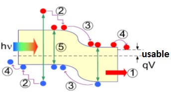
Fig. 1. Energy loss mechanism in single junction solar cell when a voltage V is applied, (1) subbandgap loss, (2) thermalization loss, (3) junction loss, (4) contact loss, and (5) recombination loss.
In addition, revolutionary breakthroughs over the last three decades reignited interest in photovoltaic research, especially on the path taken by photon energy [6]. However, among the several challenges that must be overcome to fully realize efficient photovoltaic cell confines to absorption and collection of photogenerated electrons and holes. Improved materials and device structures has been consistently modified to exercise control over photon energy distribution in photovoltaic devices [7] and can be used to reduce losses in the form of heat and enhance the pathway of energy conversion in 3rd and 4th generation photovoltaic cell.
Traditional approaches to enhance photon absorption in photovoltaic devices have involved the use of antireflection coatings to maximize transmission of incident light or photon path length within a photovoltaic cell [8]. This device structure tends to maximize the absorption of photon energy where the effects of minority carrier recombination are at minimum. The incorporation of the optical concentrator to efficiently direct incident sunlight over a large area could be used to produce a more efficient photovoltaic cell. Although a number of innovative directions have been used to enhance photon absorption, most of the techniques involve the use of sub-wavelength structures to control photon propagation in photovoltaic devices in a
wavelength-dependent manner. These approaches depend mainly on exploiting the wave nature
IJSER © 2015 http://www.ijser.org
International Journal of Scientific & Engineering Research, Volume 6, Issue 1, January-2015
ISSN 2229-5518
1942
of light to surpass classical limits of light confinement based on surface texturing [10]. The technique is appropriate because it allows for the use of thinner active layers or structures that optimizes charge collection and reduces losses in the form of heat energy in solar cells. Unique light energy absorption photovoltaic cell reported in this paper confines to tandem solar cell archtect, hot carrier, multiband solar cell and thermophotovoltaic cell as well as photonic crystal absorbers were reviewed. Furthermore, enhancement pathways of photovoltaic cell as well as light absorbers and carrier collection were also discussed.
2. TANDEM SOLAR CELL
Solar spectrum comprises of packets of energy that can be harvested at different spectral waveghtlenght. This allows the junctions to be stacked, with active layers to capture shorter wavelengths on top and longer wavelength photons passing through them to the lower layers. This approach is termed tandem solar cell (Fig. 2). A tandem approach eliminates sub-bandgap loss by using different bandgap materials. Fig. 2 shows two concepts of a tandem structure [11] using multiple cells with different bandgaps to improve overall efficiency of the photovoltaic cell. Theoretical calculations have shown that the tandem cell structure can achieve efficiency up to 86.8% under direct sunlight condition if it is stacked infinitely [12, 13, 14]. Even a small number of stacked cells can give relatively higher performance than the single junction cells. However, two stacked cell efficiency can be increased from 40.8% to 55.9% under direct irradiation. Silicon based tandem cells has been developed using amorphous/microcrystalline (a- Si/µc-Si) silicon [15]. Furthermore, a thin film polycrystalline chalcogenide based technique such as CIGS (CuInGaSe2), CdTe and CdS based cells are promising next generation solar cells.
The performance of Tandem solar cell increases as the number of cells in the stack increases, with a direct sunlight conversion efficiency up to 86.8% calculated for an infinite stack of independently operated cells [4]. However, operating each cell independently passes complication as the cells are designed with their current outputs matched to be connected in series. This constrains the cell performance as it is sensitive to the spectral content of the sunlight.
Basically, independently operating solar cells are designed to match the current across each cell connected in series and this form of connection slightly reduces the theoretical efficiency below 5 % [12,16]. The overall performance can be enhanced by short-circuiting the low-output cell to stop from consuming rather than to generate power.
IJSER © 2015 http://www.ijser.org
International Journal of Scientific & Engineering Research, Volume 6, Issue 1, January-2015
ISSN 2229-5518
1943
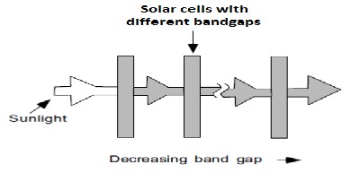
Fig. 2. Tandem cell concepts: (a) Cell stacking (b) Spectrum splitting
The concept of tandem solar cell depicted that the key loss in solar cell can be largely eliminated if the energy of the absorbed photon is adjusted a little higher than the cell bandgap. Tandem cell incorporates multiple cells with different bandgaps and are specifically tailored to convert a narrow range of photon energies (Fig. 2).
Therefore as QDs have much broader spectral absorption capability, it is expected that the deployment of QDs in could increases the device efficiency. Therefore a simple and potentially way of enhancing the efficiency of solar cell is to incorporate semiconductor such as QDs materials that absorb different spectral wavelength. This form of spectrum-shifting yields an increase in the conversion efficiency of the solar cell and can be done independently of the solar cell [4, 12 and 13]. The use of tandem solar well fit well as an enhancement pathway to increase the efficiency of a solar cell because the device split the spectrum and use semiconductor materials that optimised each section of the spectrum. Adding more devices to series of connected tandem solar cell shown in Fig. 2 enables each device to be optimized to a narrower spectrum giving a higher overall efficiency [13].
3. HOT CARRIER SOLAR CELLS
The mechanism in hot carrier solar cell (HCSC) confines to providing steady-state HC population distribution into macroscopic contacts as shown in Fig. 3. Carrier distribution integrated into selective contact regions diffuses by quasi-ballistic transport and renders the qualitative characteristics of the HCSC comparable to that of conventional solar cells. Ultrafast quasi-ballistic carrier extraction with τre ≈ 100 ps leads to hot carrier absorber (HCA) carrier densities of 1012 to 1015 cm_3 for a photon flux of 1–1000 Suns [17] with complete carrier extraction. Hall Shockley Read (HSR) recombination thus; depicts a marginal loss by high HC- SC efficiencies [17,18].
The HCSC concept utilizes selective contact to extract the hot (energetic) charge carriers before thermalization occurs. Thermalization occurs when photoexcited carriers inelastically collide with the atoms of the solar cell material. In principle, inelastic collision can be prevented by extracting the photogenerated carriers before the chances of thermalization. Electrons
IJSER © 2015 http://www.ijser.org
International Journal of Scientific & Engineering Research, Volume 6, Issue 1, January-2015
ISSN 2229-5518
1944
generated from a monochromatic short laser pulse collide in less than picoseconds and exponentially decreases the population from the band edge and is termed Boltzmann distribution [19].
This process can be grouped into different phases firstly, photoexcited electrons are distributed near the band edge, and the fermions nature prior to the collisions between electrons causes them to scatter. This collision is elastic because the same type of carriers is involved. However, there is no energy loss and the hot carrier temperature is maintained leading to broad distribution. In the next phase, collisions with the lattice atoms are dominant resulting in energy loss to the lattice and the hot carrier temperature decreases [4]. Afterwards, electrons and holes recombines and the number of carriers reduces until it reaches the initial condition. This implies that hot carrier solar cells must collect the carriers before they lose their energy by photon emission. The illustration shown in Fig. 3 depicted the conceptual design of a typical hot carrier solar cell. The absorber region represents a slow energy relaxation process and low radiative recombination rates. However, low dimensional absorber structure such as quantum dots (QDs) are preferred. A device based on hot carrier solar cell configuration have an efficiency comparable to the infinite tandem structure [19].
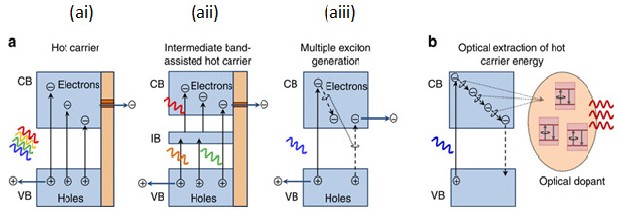
Fig.3 Three hot-carrier solar-cell design comprising a direct extraction of hot carriers through energy- selective contacts (ai), application of an intermediate-band-assisted absorber (aii) and using multiple exciton generation (aiii) as hot carrier induces additional excitations across the bandgap. (b) The concept of optical extraction is illustrated depicting hot carriers transfer of their excess energy to nearby Er3+ ions and afterwards subsequently emit infrared (IR) photons. Valence band (VB), conduction band (CB) and intermediate band (IB) were respectively represented.
Devices based on hot carrier solar cell allows electron or hole to gains sufficient kinetic energy to overcome a potential barrier necessary to break an interface state. However, "hot" as used to explain charge carriers refers to the effective temperature utilized to exemplify carrier density nevertheless; this does not depict the overall temperature of the device [16]. However, different time constants can be appreciated by imagining a direct bandgap cell illuminated by a short pulse of a monochromatic light source such as laser to create electrons in the conduction
band and holes in the valence band of distinct energy [18]. Collisions of these carriers occur in
IJSER © 2015 http://www.ijser.org
International Journal of Scientific & Engineering Research, Volume 6, Issue 1, January-2015
ISSN 2229-5518
1945
less than a picosecond and tends to spread over the distribution of light. The peaked distributions could become more broader comparable to the Boltzmann type of distribution. However, elastic collision of carriers of the same type do not result to any loss of energy. The hot carrier temperature distribution can be determined using the total number of carriers that was created by the laser pulse and the energy of each carrier. Differences in temperature are possible only for electrons and holes with different energy [20]. The efficiency of this approach is 86.8% as in tandem cell stack. To achieve this, the efficiency of the carrier cooling rate must be sufficiently reduced or the radiative recombination rate must be adequately increased in such a way the latter becomes faster than the initial stage.
However, a standard solar cell could be designed to collect carriers before recombination stage of decay sequence. The idea behind using a hot carrier solar cell is to capture the carriers before cooling. Based on the hot carriers technique, the carriers are either made to traverse the cell very quickly or slows the cooling rate. Therefore a special contacts to prevent cooling the carriers is needed [20, 21]. This is attainable only if the rate of radiative recombination of electrons generated by energetic photons is faster than cooling rates, thus frequency conversion occurs and can potentially improve the solar cell efficiency [22].
Carrier cooling in bulk semiconductors occurs between 10–100 ps, (see Fig. 4). Optical
produces carriers instantaneously and generates carrier population areas of photon flux and HCA electronic density of state (DOS). Electrons specifically have individual energies and do not interact except for spinning election rules. Electron interacts at 10–100 fs as a result of elastic scattering leading to energy re-normalization for hot electrons or to impact ionization of valence band electrons (Auger generation). This is a reverse process where the energy released re-heats the free electron. Energy re-normalization result to Fermi–Dirac electron population without generating additional phonons, the lattice is in thermal equilibrium [23].
Electron–optical phonon (Frohlich) interaction generated from local electrostatic lattice distortion forms photon cloud often refer to as polarons. In contrary, quantization of vibrational lattice excitation yields optical phonons thus; electron energy loss by optical phonon emission and decays into acoustic phonons and so re-heat free electrons as shown in Fig. 4 and Fig. 5 respectively. The emission and decay of optical phonon elapses until the electrons thermalizes. Acoustic phonons heat affects quasi-ballistic carrier transport and free carriers yield to direct (radiative) and indirect (Hall Shockley Read (HSR)) recombination. However, photonsgenerated radiative could be re-absorbed via ground state transition or free carriers-absorption. HSR recombination is at least three orders of magnitudes lower than electron cooling [23].
Reducing the energy quantum ħωo of optical phonons delays carrier cooling. Optical phonon emission occurs in a short, yet finite time. Lower ħωo, electrons emit more optical phonons for a certain lost energy. However, minimum ‘ħωo can be attained by a binary compound with larger mass for a lighter atom as evidenced from the ω (k) dispersion of 1d diatomic link where ω+ and ω- (rad -1 s_1), γ (Nm_1), mb and ms (kg), µ m (kg) and a (m) explains the optical and acoustic phonon chain, the constant force of the vibrating bonds, heavy and light atom masses, mass reduction of the oscillating system and the length of the 1d unit cell; two bond lengths for a diatomic chain are presented [8].
Electrons excited form polarons have radii ranging between 20–90Å for the majority of the solids [24]. Frohlich interaction explains electron optical phonon coupling in solids with
IJSER © 2015 http://www.ijser.org
International Journal of Scientific & Engineering Research, Volume 6, Issue 1, January-2015
ISSN 2229-5518
1946
large dielectric constant ɛrel and low electron effective mass mneff and Frohlich constant αFro is small [24]. Low mneff reduces electron momentum and lead to small atomic elongation. However, this effect enhances hot carrier generation using the free electron energy is E (e-) = (ħk)2 / mneff. In the other hand, the electrostatic screening with large ɛrel tends to decrease polaron radius as well as the number of atoms that are affected. Based on this fact, covalent solids are preferably used as the dipole moment for small atomic bonds.


± = y 1
μ
1 2

±
μ

4
s
ak

s n 2 ( )
2

With reduced effective mass µ m = mbms
mb+ms
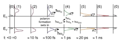
Fig. 4. Carrier cooling kinetics in bulk semiconductor: Thermal equilibrium (0); immediately after optical generation (1); carrier scattering, impact ionization, re-normalization of carrier energies, Fermi–Dirac statistics (2);optical phonon emission(re-absorption) (3); decay of optical into acoustic phonons (4);
further phon 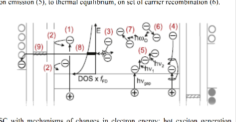
Fig. 5. HC- (1) reflected
electronsat ESC, (2) energy re-normalization by electron-scattering, refilling DOS subject to carrier extraction (3), impact ionization (4),free electron re-absorption of sub-bandgap photons(5), optical
IJSER © 2015 http://www.ijser.org
International Journal of Scientific & Engineering Research, Volume 6, Issue 1, January-2015
ISSN 2229-5518
1947
phonon emission, (6) re-absorption, (7) quasi-ballistic transport, (8) energy selective tunneling from
HCA(9).
4. MULTIBAND SOLAR CELLS
Traditionally, solar cells depends on the excitation between valence and conduction band. However, if a third band comprising of impurity band is incorporated into the cell framework (Fig. 6.), the efficiency of the device increases [25]. This concept has been extended to include n- band cell and necessitated for an additional implementation approaches. The theory encompasses using excitation between the mini bands of superlattices and phonon relaxation processes can be controlled using semiconductors with multiple narrow bands compounds or high concentration of impurities to form multiple impurity bands in a wide bandgap semiconductors. It then implies that the approach is compatible with spectral variations of sunlight [26].
Multiband solar cells improves power conversion efficiencies of 3rd and 4th generation solar cells using intermediate bands to collect less photon energy. This process increases the absorption wavelength of photovoltaic devices. Theoretically, myriads of constrain impede the efficiency of impure solar cells [27, 28] yet, the three band structure solar cell offers an efficiency of 63.2% while with four band structures, increase up to 71.7%. Fig. 4 shows the concept of a multiband solar cell and its equivalent circuit diagram. The multiband solar cell can be fabricated using wide bandgap nanomaterial. Adding impurity without relaxation in a small bandgap semiconductor could reduce the performance of the device however; using materials with bandgap energy from 1.6eV is preferred [29, 30].
The concept of multiband solar cell presents an alternative to multi-junction designs for
enhancing power conversion efficiency of solar cells. The intermediate band acts as a “stepping stone,” allowing absorption of photons at three different energy levels, corresponding to the three different band gaps. The low-energy photons which cannot be trapped by conventional solar cell are captured using multiband solar cell (Fig. 6).
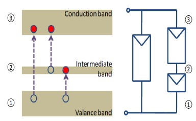
Fig. 6 Band diagram (left) and Equivalent circuit diagram (right) of a multiple band solar cell containing three bands.
IJSER © 2015 http://www.ijser.org
International Journal of Scientific & Engineering Research, Volume 6, Issue 1, January-2015
ISSN 2229-5518
1948
Extending the bandgap of nanostructured materials to infrared provides the opportunity to transform infrared light energy into electricity. This attractive option could harvest more light energy since nearly half of the approximately 1000Wm3 of sunlight is within the invisible infrared region. Therefore, visible light can be used for direct lighting while the invisible part can be harvested for generating electricity [3]. Photovoltaic devices that utilizes infrared is referred to as ‘thermovoltaics’ can fuel-fire emitter and co-generation of electricity as well as heat energy sources. Theoretically, solar cells based on this concept are more efficient than traditonal silicon cell in direct sunlight. In addition, using a light-sensitive conjugated polymers has added to the attractiveness of infrared photovoltaic with alternating single and double carbon-carbon bonds. Doping of the conjugated polymers potentially increases the electronic conductivity of the nanostructured materials in several orders of magnitude [3, 4]. This stands out as an alternative enhancement pathway to harvest light energy using a low cost, flexibility nanostructured material such as poly (2-methoxy-5-(2’-ethylhexyloxyp-phenylenevinylene)] (MEH-PPV) that absorbs between ~400 and ~600 nm, QDs of lead sulphide (PbS) absorption can be tuned from ~800 to ~2000 nm. Coating of MEH-PPV on the QDs could shift the polymer’s absorption into the infrared region [28].
Multiband solar cell enhanced photon absorption with the donor and acceptor separated on a length scale that is not proportional to the efficient exciton diffusion. Most probably, a light trapping strategy that is compatible with the multiband architecture using donor and acceptor polymers phase are used to separate intermixed nanostructure of a low-index photonic crystal such as zinc oxide (ZnO) or titanium dioxide (TiO2) into a bulk heterojunction matrix. Photon absorption based on multiband based on organic photovoltaic (OPV) absorbers have been theoretically studied [31 – 33]. Using plane-wave transfer and scattering matrix simulations, absorption improves 17% using an optimized planar structure of the photonic crystal solar cell. However, simulations depicted reduction in the distance between exciton generation and separation and suggests a favorable electrical properties and higher absorption [32]. The modal character of the enhancement of the absorption profile and the photonic band structure of the absorber layer shows that both broad-band and narrow-band modes exist with short and long lifetimes. It is noteworthy that not all the modes lead to absorption enhancement as some are optically inactive. Light concentration in quasi-guided modes at the lower part of a photonic crystal without a spacer layer leads to trapping of light in the electrode material instead of the active layer and reduces light absorption [34].
Ko et al [35] fabricated an organic solar cells using photonic active crystal layer using a low efficiency TDPTD:PCBM system incorporated with a non-wetting perfluoropolyether mold to form hexagonal columns of 180 nm high and a periodicity of 400 nm. The columns contains 5 nm size ZnO nanoparticles and the thickness was tuned to provide index contrast in the photonic crystal and an optical spacing layer for the interference effects of light. The device has a higher absorption than planar device at wavelengths exceeding 600 nm. The incident photon-to-electron conversion efficiency, improved over the entire spectrum of the absorbing layers and improvement in the internal quantum efficiency. This immensely contributed towards the enhancement of electrical performance, which could further be enhanced by aligning the grain or by modifying the exciton creation and dissociation profile [36 – 39]. P3HT:PCBM materials
IJSER © 2015 http://www.ijser.org
International Journal of Scientific & Engineering Research, Volume 6, Issue 1, January-2015
ISSN 2229-5518
1949
incorporated with a copper phthalocyanine layer absorbs 90% photon energy out of which 13% efficiency enhancement comes from photonic crystal. Crystalline silicon and amorphous silicon photonic crystal layer comprising of stripes [42 – 44], nanopillars and nanorods [40, 41], nanowells and nanoholes [42, 45 – 47] and conical nanowells [48] investigated theoretically and experimentally for solar cell applications improves photon absorption and short circuit current density by coupling to quasi-guided modes in the layer. This finding is consistent with the theory of Yu et al., [49] depicting that low index material incorporated with a high index absorber layer significantly improve absorption. However, in practice, passivation of etched devices and electrical problems poses challenges towards increasing the conversion efficiency of patterned silicon photonic crystal layer [49].
5. THERMOPHOTOVOLTAICS
Thermophotovoltaics is an established type of photovoltaics that utilizes light from a heated source rather than the sun to generate electricity [50]. They could be refer to as power generating systems consisting a heat soure, an emitter and a photovoltaic power converter. The operating principles is comparable to traditional photovoltaic but is incorporated with additional components such as concentrators, filters and reflectors that exponentially enhance light output source of a device that generate the light by band-to-band recombination which is of advantage to the cell performance [41]. Fundamentally, the heated device operates like an emitter of narrow bandwidth light with specific energy, kT of its bandgap energy. In this case, monochromatic light can be efficiently converted by a solar cell and light emitted by the solar cell can be recycled back to drive the light-emitting diode. This is conveniently achieved because, the same current flows through the cell and the source diode. Therefore, the voltage across the diode tends to be smaller than that across the cell when the diode is subjected to higher temperature leading to power dissipation in the load [26].
Advances in thermophotovoltaics approach follows the concepts of an emitter above the low-bandgap solar cell. The heated body can generate narrow and low light energy from heat source rather than the sun. There are two reasons that lead to high efficiency [29] firstly, the heat source emit a narrower bandwidth light than the sun spectrum by using rare-earth elements; secondly, the energy from the cell such as that reflected or emitted as light and recycled back to the heat source. The heated body serves as an emitter of narrow bandwidth light suitable for the small bandgap solar cell. This narrow light is efficiently converted using cell which optimizes the emitted energy. This concept has power conversion efficiency of 85.6% in principle [30], if used to convert solar radiation in conjunction with a thermal absorber.
In principle, thermophotovoltaic (TPV) energy conversion depicts a direct conversion process from heat to electricity via photons. Device based on this form of power generation system recovers exhaust heat from different heat sources such as heat engines and ironwork rolling processes. TPV system typically consists of an IR solar cell and a thermal emitter as the heat/light converter as shown in Fig. 5. The thermal emitter enhances the emission spectrum of the heat source to match the absorption wavelength of the solar cell [51]. Under ideal situation, the maximum emissivity correspond to the wavelength the solar cell absorption is maximum. In general, the shape of a thermal radiation spectrum depends on its temperature. As the
IJSER © 2015 http://www.ijser.org
International Journal of Scientific & Engineering Research, Volume 6, Issue 1, January-2015
ISSN 2229-5518
1950
temperature increases, the radiation power increases and the peak wavelength is shifted toward the blue end of the spectrum.
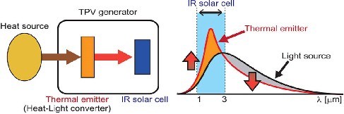
Fig. 5 Schematic portrayal of thermophotovoltaic (TPV) system
The concept of thermophotovoltaics allows photonic crystal layer to be used to structure the absorption spectrum of emission spectra by absorbing concentrated higher energy photons from sunlight such that emissivity at longer wavelengths is suppressed to prevent re-emission. The absorber is thermally coupled to a narrow-band emitter that closely matched the absorption of a low-bandgap semiconductor and in this case, functions as selective, temperature stable absorbers and emitters [51 – 54] for photon enhancement with the PV diode [55].
6. PHOTONIC CRYSTAL ABSORBERS
Photonic crystals are used to tailor the absorption spectrum of material by trapping and localizing light energy within the photonic crystal. This process enhances the path length of light frequencies [46]. The interaction between electron and the periodic potential results in the formation of energy bandgaps. However, the presence of defects in the periodicity of the lattice can locally disrupt the bandgap giving way to interesting electronic properties [43]. Formation of light absorbers that are structured as photonic crystals has drawn much research interest that lends itself to the design of organic solar cell [23]. The absorption length and the exciton diffusion length in such devices respectively differ by an order of magnitude (100s vs. 10s of nm, [56]. Strong light absorption by thinner layers of the active semiconductor material, especially in wavelengths close to the infrared absorption edge are desired [57]. Using Finite Difference Time Domain (FDTD) simulations of electromagnetics based on Maxwell’s equations achieved 35.6% absorption enhancement by optimizing a 500 nm periodicity, 400 nm wire diameter and 150 nm layer thickness. This structure shows a high density of Bloch modes, two Bloch modes for coupling normally incident light and a long modal lifetime very near the absorption edge basically because of low group velocity evidenced by slowly propagated light in the dispersion relation at the relevant wavelengths (600 – 700 nm) [33]. This implies that the calculation of the electromagnetic field values reduces discrete steps in time and gives broadband output from a single execution and provides an excellent scaling performance.
IJSER © 2015 http://www.ijser.org
International Journal of Scientific & Engineering Research, Volume 6, Issue 1, January-2015
ISSN 2229-5518
1951
6.1 Enhancement Pathway for Photovoltaic Cell
Proper utilization of one hour of sunlight could sufficiently provide world energy need in a year. Because the sun’s energy is free much interest has been devoted in solar energy as a major contributor to green energy [58]. Solar energy can significantly contribute in reducing the cost of power generation using high refractive index (n) of inorganic semiconductor materials leading to high optical reflectivity at a direct, planar interface between a semiconductor and a low-index medium such as air or glass as shown in Fig. 6a. Because there is no reflected light available to be converted into electricity in a solar cell, strategies to reduce reflectivity are essential factors towards the enhancement photon pathway in photovoltaic devices.
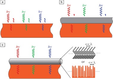
Fig. 6. Reduction of incidence reflection light in photovoltaics. (a) At a planar interface between air or glass and a typical semiconductor photovoltaic material, a reasonable fraction of incident light depicted by photon energy (hν) is reflected as a result of a mismatch in refractive index at the interface. (b) A dielectric film with suitable thickness and refractive index can reduce reflection of light at specific wavelength including normal incident light and reduce reflection over a wide range of wavelengths. (c) A dielectric filmwith a continuous refractive index similar to that of air or glass is used at the upper interface while the underlying semiconductor material at the bottom act as an effective antireflection coating over the range of wavelengths and incident angles of light that is appropriate for photovoltaic devices.
Advances in the fabrication of nanostructures enable the control of surface reflectivity of photovoltaic devices. For instance, graded-index coating that is finely stepped can be used to increase the refractive index from an external medium such as air to the photovoltaic device surface and additionally, provides a functional anti-reflection over a wide range of wavelengths and incident angles (59-61). This could be because the absence of an interface from which light can reflect thus, light is transmitted across various refractive indexes. The innovative deposition technique used for processing material surfaces has enabled the realization of graded-index coatings using surface structures with features comparable to or smaller than the wavelength of incident light at length scales and shape. This makes it possible for the material to effectively
IJSER © 2015 http://www.ijser.org
International Journal of Scientific & Engineering Research, Volume 6, Issue 1, January-2015
ISSN 2229-5518
1952
provide a fine stepped increase in refractive index comparable to air and the photovoltaic material such as (62-63) as illustrated in Fig. 6c. This approach has been illustrated by Kuo et al. [64] using angled deposition of dielectric films to create a sub-wavelength scale of nanorods within the film. The refractive index of the film was reduced from that of bulk materials by a factor that is equal to the fractional volume occupied by the nanorods by allowing for effective refractive indices lower than the bulk dielectric material comparable to that of air [65-66]. The customizable surface features of QDs semiconductors such as CdSe PbSe, CdS and CdTe could provide an alternative pathway towards enhancing the reflective indices of photovoltaic devices by using different particle sizes to the emitted light energy of different wavelength.
Because the index of refraction is a function of the amount of the material use of air, there is need for a smooth transition from a low refractive index comparable to air to that of material and for an ultralow-reflectivity surface [67]. This approach could be explored to establish a low reflectivity surfaces for a more efficient solar cell by effectively increasing the path length of photons within the absorbing medium [68].
6.2 Light Absorption and Carrier Collection
Mallick et al. [69] describes patterning of a thin-film photovoltaic device into a two-dimensional photonic crystal structure leading to coupling of incident photons into a confined mode with photonic crystal. Effective scattering and trapping of light (Fig. 7a,b), within the device increases photocurrent response over a wide range of wavelength.
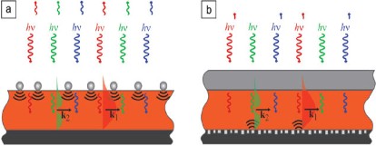
Fig. 7 For thin-film photovoltaic devices: micrometer-scale texturing is challenging, however, an alternative light trapping approach has emerged. (a) Metal and/or dielectric nanostructures on the device surface can scatter incident light into optical modes labeled k 1 and k 2, confined within the thin-film semiconductor device structure. Such scattering effect can provide photons energy with increased path lengths leading to increase in optical absorption efficiency within the device. (b) Scattering of light into waveguide modes in a thin-film of photovoltaic device such as QDs can be achieved by scattering structures on the back side of the device. This geometry could allow scattering to be optimized for longer- wavelength light using low optical optical absorption coefficients is typically lower, and enables integration of an antireflection coating on the top surface.
The structure further describes the use of multilayer dielectric stacks and metal nanostructures for light trapping. Plasmonics particles have shown promising route to enhance
IJSER © 2015 http://www.ijser.org
International Journal of Scientific & Engineering Research, Volume 6, Issue 1, January-2015
ISSN 2229-5518
1953
photon absorption in photovoltaics [70, 71]. Plasmons are collection of excited electrons in materials with high electron densities is produced by the interaction of light energy with metal dielectric materials. The excitations can be produced in bulk material while surface plasmon mostly occurs at the surfaces and interfaces [72]. Surface plasmons can be used to confine light energy in spaces that is shorter than one-fourth of the wavelength of the light to produce an enhanced pathway to 3rd and 4th generation photovoltaic in many orders of magnitude utilizing its strong optical fields. This strategy has been used in analytical chemistry for surface enhancement of Raman spectroscopy. This is because the surface plasmon modes are very sensitive to surface profile of material and the surrounding dielectric environment to form nanoparticles therefore their integration with metallic material in solar cells can strongly enhance photon absorption. However, their usefulness in bulk crystalline [73-74], and thin-film photovoltaics and photodetectors has been reported [75-78]. Plasmonic absorption increases electromagnetic field amplitude and optical transition probability within several nm in nanoparticle. The emergence of plasmonic excitation plays an important role in improving the photoresponse and can be applied to the QDSSC using platinum electrode. Plasmonic effects in such devices, metal nanostructures should be located in close proximity away from the device active structure [79, 80].
The plasmonic scattering effects in metals and dielectric nanostructures can be exploited to enhance the optical absorption in thin-film photovoltaic devices such as QDSSC. Catchpole et al.’s [81] use plasmonic concept to improve the performance of photovoltaic device. The enhancement pathway of photon energy in photovoltaics devices is based on the system and not at the device itself, especially on devices using optical concentrators to focus light incident over a large area onto smaller efficient photovoltaic cells [82]. The use of concentrators in photovoltaic systems provide a competitive edge to directly addressed emerging developments technologies such as microscale [80] and luminescent concentrators [83] which is intriguing and promising possibilities for the development of a cost effective solar energy harvesting strategy for 4th generation photovoltaics devices.
7. CONCLUSION
The enhancement pathways of light energy absorption that confines to the concepts of 3rd and 4th generation photovoltaic cells to realize efficient photovoltaic cells have been reviewed. Light energy absorption pathways confines to tendam solar cell concept, hot carrier solar cell, multiband solar cell and Thermophotovoltics. Tendam solar cell allows the use of semiconductor material with broader spectral absorption capability such as QDs. This concept can potentially increase device efficiency by absorbing different spectral wavelength. This form of spectrum- shifting capability of device materials yields an increase in the conversion efficiency of the solar cell. In the other hand, devices based on hot carrier solar cell allows electron or hole to gains sufficient kinetic energy to overcome a potential barrier necessary to break an interface state. However, extending the bandgap of nanostructured materials to infrared provides unique opportunity to transform infrared light energy into electricity. This concept is compatible with multiband solar cell and depicts an alternative to multi-junction designs for enhancing power conversion efficiency of solar cells. The efficiency of device can be boosted using the intermediate band which supports absorption of light energy at three different energy levels, corresponding to the three different bandgaps.
IJSER © 2015 http://www.ijser.org
International Journal of Scientific & Engineering Research, Volume 6, Issue 1, January-2015
ISSN 2229-5518
1954
In addition, the concept of TPV energy conversion utilizing heat source to generate electricity holds the potential to enhance photovoltaic conversion efficiency. Device based on this concept recovers exhaust heat from different heat sources such as heat engines and ironwork rolling processes and consists of an IR solar cell and a thermal emitter as the heat/light converter. The thermal emitter is used to enhance the emission spectrum of the heat source to match the absorption wavelength of the solar cell. These light energy enhancement options paves way for an increase in efficiency for 3rd and 4th generation photovoltaic cell.
However, a number of innovative directions for efficient photon absorption have been reported in the present study. Options reviewed in this work can be applied independently to suit specific design and are compatible with customizing spectral absorption wavelength to control photon propagation of the photovoltaic devices in a wavelength-dependent manner. Another common feature of these approaches is suitable for exploiting the wave nature of light to surpass classical limits of light confinement based on surface texturing which are compatible with 3rd and
4th generation solar cells. Various light energy absorption pathways depicts potential strategy to efficiently harvest and utilized photon energy in a way to improve the performance of photovoltaic cell. Research in this direction provides several options to configure light absorption capability of devices to enhance the performance of various photovoltaic cell architect. Therefore, future photovoltaic device require smart material selection to reduce wastages in form of loss of energy in form of heat. Additionally, interface properties of photovoltaic device especially those incorporating multiple layers of absorber should be carefully patterned to ensure unobstructed charge flow.
REFERENCES
[1] Schlesinger, S. H., Schneider, R. G., Watts, T., Wigley, M. L., Wuebbles, D.J.1998. "Energy implications of future stabilization of atmospheric CO2 content," Nature, 395, 881-884.
[2] "Basic Research needs for Solar Energy Utilization 2005. Report on the basic energy
Sciences Workshop on Solar Energy Utilization, April 18-21 2005.
[3] Solar Energy Technologies Program: Multi-Year Technical Plan 2003-2007 and Beyond,
2004.
[4] Nozik, A. J. 2010. Nanoscience and nanostructures for photovoltaics and solar fuels. Nano
Lett. 10, 2735–2741.
[5] Landsberg, P.T., Baruch, P., 1989. "The thermodynamics of the conversion of radiation energy for photovoltaics," Journal of Physics A: Mathematical and General, vol. 22, pp. 1911-
1926.
[6] J. Zhao, A., Wang, F., Yun, G., Zhang, D., Roche, M., Wenham, S.R., Green, M.A. 1997. "20,000 PERL silicon cells for the "1996 World Solar Challenge"," Progress in Photovoltaics. 5,
269-276,.
[7] McIntosh, K., Cudzonovic, M., Smith, D., Mulligan, W. Swanson, R. 2003. "The choice of silicon waferfor the production of rear-contact solar cells. ," in 3rd World Conference on Photovoltaic EnergyConversion, Osaka. 971-974.
[8] Maruyama, E., Terakawa, A., Taguchi, M., Yoshimine, Y., Ide, D., Baba, T., Shima, M., Sakata, H., Tanaka, M. 2006. "Sanyo's challenges to the development of high-efficiency HIT
IJSER © 2015 http://www.ijser.org
International Journal of Scientific & Engineering Research, Volume 6, Issue 1, January-2015
ISSN 2229-5518
1955
solar cells and theexpansion of HIT business," in 4th World Conference on Photovoltaic Energy
Conversion (WCEP-4), Hawaii,. 729-732.
[9] Xi, J.Q., Schubert, M.F., Kim, J.K., Schubert, E.F., Chen, M.F., Lin, S.Y., Liu , W., Smart, J.A. 2007. Optical thin-film materials with low refractive index for broadband elimination of Fresnel reflection. Nat. Photonics 1: 3, 176-179.
[10]. Kuo, M.L., Poxson, D.J., Kim, Y.S., Mont, F.W., Kim, L.K., Schubert, E.F., Lin , S.Y.
2008. Realization of a near-perfect antireflection coating for silicon solar energy utilization. Opt. Lett. 33 , 2527-2529.
[11] Jackson, E.D. 1960. US Patent, 2,949,498.
[12] Marti, A., Araujo, G.L. 1996. "Limiting efficiencies for photovoltaic energy conversion in multigap systems," Solar Energy Materials and Solar Cells. 43, 203-222..
[13] Vos, A.D. 1980. "Detailed balance limit of the efficiency of tandem solar cells," Journal of
Physics D: Applied Physics, 13, 839-846.
[14] Green, M.A. 2003. "Thin-film photovoltaics, An annual Review of Research and
Development," in Advences in Solar Energy: Americal Solar Energy Society, 187-214.
[15] Green, M.A. 2001. Third Generation Photovoltaics:Advanced Solar Conversion. Sydney: Center forPhotovoltaic Engineering, University of New South Wales.
[16] Hanna, M.C., Lu, Z., Nozik, A. J. 1997. "Hot Carrier Solar Cells," AIP Conf. Proc., Future
PVGeneration Technologies, vol. 404, pp. 309-316.
[17] Bruton, T.M., Luthardt, G., Rasch, K.D., Roy, K., Dorrity, I.A., Garrard, B., Teale, L., Alonso, J., Ugalde, U., Declerq, K. J., Nigs, J., Szlufcik, A., Rauber, W., Wettling, A., Vallera, A. 1997. study of the manufacture at 500 MWp p.a. of crystalline silicon photovoltaic modules, Conference Record, 14th European Photovoltaic Solar Energy Conference, Barcelona, June, 11–
16.
[18] Takeda, Y., Motohiro, T. 2012. Intermediated-band-assisted hot-carrier solar cells using indirect-bandgap absorbers. Prog. Photovolt. Res. Appl. 21, 1308–1318 (2012).
[19] Brown, A.S., Green, M.A., Corkish, R.P. 2002. "Limiting efficiency for a multi-band solar cell containing three and four bands," Physica E: Low-dimensional Systems and Nanostructures,
14, 121-125.
[20] Ross, R.T., Nozik, A.J. (1982). Efficiency of hot-carrier solar energy converters. Journal of
Applied Physics, 53, 3813-3818.
[21] Würfel, P. 1997. Solar energy conversion with hot electrons from impact ionization. Sol. Energy Mater. Sol. Cells. 46, 43–52.
[22] Vassiltsova, O.V., Panda, S.K., Zhao, Z., Carpenter, M.A., Petrukhina, M. A., 2009. Ordered fabrication of luminescent multilayered thin films of CdSe quantum dots.” Dalton Trans. 9426–9432.
[23] K¨onig, D., Casalenuovo, K., Takeda, Y., Conibeer, G., Guillemoles, J. F., Patterson. R.
2010. Hot carrier solar cells: Principles, materials and design. Physica E, doi:10.1016/j.physe.2009.12.032
[24] Shockley, W. & Queisser, H. J. 1961. Detailed balance limit of efficiency of p–n junction
solar cells. J. Appl. Phys. 32, 510–519.
IJSER © 2015 http://www.ijser.org
International Journal of Scientific & Engineering Research, Volume 6, Issue 1, January-2015
ISSN 2229-5518
1956
[25] Miritello, M., Salvio, R. L., Cardile, P., Priolo, F. 2010. Enhanced down conversion of photons emitted by photoexcited ErxY2-x Si2O7 films grown on silicon. Phys. Rev. B 81,
041411
[26] Green, M. A. Third Generation Photovoltaics Springer (2003).
[27] Luque, A. Marti, A. 1997. Increasing the Efficiency of Ideal Solar Cells by Photon Induced
Transitions at Intermediate Levels Phys. Rev. Lett. 78: 26, 5014–5017.
[28] Zhao, J., Wang, A., Green, M. A. 1999. "24.5% efficiency silicon PERT cells on MCZ
ubstrates and 24.7% efficiency PERL cells on FZ substrates," Progress in Photovoltaics, 7, 471-
474.
[29] Coutts, T., 2001. In Clean Electricity from Photovoltaics; Vol. 1, edited by M. Archer and
R. Hill (Imperial College Press, London, England, 481-528..
[30] Hanna, M.C., Nozik, A. J. 2006. "Solar conversion efficiency of photovoltaic and hotoelectrolysis cells with carrier multiplication absorbers," J.of App. Physics, 100, 074510-
074518.
[31] Tumbleston, J.R., Ko, D.H., Samulski, E.T., Lopez, R. 2009. Electrophotonic enhancement of bulk heterojunction organic solar cells through photonic crystal photoactive layer. Appl Phys Lett. 94: 4, 043305.
[32] Tumbleston JR, Ko D-H, Samulski ET, Lopez R. Absorption and quasiguided mode analysis of organic solar cells with photonic crystal photoactive layers. Opt Express 2009; 17 (9):
7670 – 81.
[33] Chen, L., Sha, W.E.I., Choy, W.C.H. 2012. Light harvesting improvement of organic solar cells with self-enhanced active layer designs. Opt Express 20: 7, 8175 – 8185.
[34] Duché, D., Drouard, E., Simon, J., Escoubas, L., Torchio, P., Le Rouzo, J., Vedraine, S.
2011. Light harvesting in organic solar cells. Sol Energ Mat Sol Cells 95, S18– S25.
[35] Ko, D.H., Tumbleston, J.R., Zhang. L., Williams, S., DeSimone, J.M., Lopez, R., Samulski, E.T. 2009. Photonic crystal geometry for organic solar cells. Nano Letters 9: 7, 2742 – 2746.
[36] Hlaing, H., Lu, X., Hofmann, T., Yager, K.G., Black, C.T., Ocko, B.M. 2011. Nanoimprint- induced molecular orientation in semiconducting polymer nanostructures. ACS Nano. 5: 9, 7532
– 7538.
[37] Shih, C.F., Hung, K.T., Wu, J.W., Hsiao, C.Y., Li, W.M. 2009. Efficiency improvement of blended poly(3-hexylthiophene) and 1-(3-methoxycarbonyl)-propyl-1-phenyl-(6,6)C[sub 61] solar cells by nanoimprinting. Appl Phys Lett. 94: 14, 143505.
[38] Lee, J.H., Kim, D.W., Jang, H., Choi, J.K., Geng, J., Jung, J.W., Yoon, S.C., Jung, H.T.
2009. Enhanced solar-cell efficiency in bulk-heterojunction polymer systems obtained by nanoimprinting with commercially available AAO membrane filters. Small (Weinheim an der Bergstrasse, Germany) 5: 19, :2139 –2143.
[39] Chou, W.Y., Chang, J., Yen, C.T., Tang, F.C., Cheng, H. L., Chang. M.H., Lien-Chung
Hsu, S., Chen, J.S., Lee, Y.C. 2011. Nanoimprinting-induced efficiency enhancement in organic solar cells. Appl Phys Lett. 99: 18, 183108.
IJSER © 2015 http://www.ijser.org
International Journal of Scientific & Engineering Research, Volume 6, Issue 1, January-2015
ISSN 2229-5518
1957
[40] Alaeian, H., Atre, A.C., Dionne, J.A. 2012. Optimized light absorption in Si wire array solar cells. J Opt .14: 2, 024006.
[41] Chutinan, A., Kherani, N.P., Zukotynski, S. 2009. High-efficiency photonic crystal solar cell architecture. Opt Express. 17: 11, 8871 – 8878.
[42] Meng, X., Depauw, V., Gomard, G., El Daif, O., Trompoukis, C., Drouard, E., Jamois, C.,
Fave, A., Dross, F., Gordon, I., Seassal, C. 2012. Design, fabrication and optical characterization of photonic crystal assisted thin film monocrystalline-silicon solar cells. Opt Express 20, A465 – A475.
[43] Park, Y., Drouard, E., El Daif, O., Letartre, X., Fave, A., Kaminski, A., Lemiti, M., Seassal, C., De Lyon, U., De Lyon, N., Insa-ecl-ucbl, U.M.R.C. 2009. Absorption enhancement using photonic crystals for silicon thin film solar cells. 17: 16, 14312 – 14321.
[44] Zanotto, S., Liscidini, M., Andreani, L.C. 2010. Light trapping regimes in thin-film silicon solar cells with a photonic pattern. Opt Express. 18: 5, 4260 – 4274.
[45] Mallick, S.B., Agrawal, M., Wangperawong, A., Barnard, E.S., Singh, K.K., 2012. Ultrathin crystalline-silicon solar cells with embedded photonic crystals Ultrathin crystalline-silicon solar cells with embedded photonic crystals. 053113, 1 – 4.
[46] Meng, X., Gomard, G., El Daif, O., Drouard, E., Orobtchouk, R., Kaminski, A., Fave, A., Lemiti, M., Abramov, A., Roca, I., Cabarrocas, P., Seassal, C. 2011. Absorbing photonic crystals for silicon thin-film solar cells: Design, fabrication and experimental investigation. Sol Energ Mat Sol Cells. 95, S32 –S38.
[47] Han, S.E., Chen, G. 2010. Optical absorption enhancement in silicon nanohole arrays for solar photovoltaics. Nano Letters. 10: 3, 1012 – 1015.
[48] Du, Q.G., Kam, C.H., Demir, H.V., Yu, H.Y., Sun, X.W. 2011. Enhanced optical absorption in nanopatterned silicon thin films with a nano-cone-hole structure for photovoltaic applications. Opt Letters. 36: 9, 1713 – 1715.
[49] Yu, Z, Raman, A., Fan, S. 2010. Fundamental limit of nanophotonic light trapping in solar cells. Proc Natl Acad Sci USA 107: 41, 17491 – 17496.
[50] Green, M.A. 2001. Third generation photovoltaics: Ultra-high conversion efficiency at low cost. Progress in Photovoltaics: Research and Applications 9, 123-135.
[51] Rephaeli, E., Fan, S., 2009. Absorber and emitter for solar thermophotovoltaic systems to
achieve efficiency exceeding the Shockley-Queisser limit. Opt. Express 17: 17, 15145 – 15159. [52] Yeng, Y.X., Ghebrebrhan, M., Bermel, P., Chan, W.R., Joannopoulos, J.D., Soljačić, M., Celanovic, I. 2012. Enabling high-temperature nanophotonics for energy applications. Proc. Natl. Acad. Sci. USA. 109: 7, 2280 –2285.
[53] Arpin, K.A, Losego, M.D., Braun, P.V. 2011. Electrodeposited 3D tungsten photonic crystals with enhanced thermal stability. Chem Mater 23: 21, 4783– 4788.
[54] Araghchini, M., Yeng, Y.X., Jovanovic, N., Bermel, P., Kolodziejski, L.A., Soljacic, M, Celanovic, I., Joannopoulos, J.D. 2011. Fabrication of two-dimensional tungsten photonic crystals for high-temperature applications. J Vac Sci Technol B Microelectronics Nanometer
Struct 29: 6, 061402.
IJSER © 2015 http://www.ijser.org
International Journal of Scientific & Engineering Research, Volume 6, Issue 1, January-2015
ISSN 2229-5518
1958
[55] Shemeya, C, Vandervelde, T.E. 2012. Comparison of photonic-crystalenhanced thermophotovoltaic devices with and without a resonant cavity. J Electron Mater 41: 5, 928 –
934.
[56] Coakley, K.M., McGehee, M.D., 2004. Conjugated polymer photovoltaic cells. Chem Mater
16: 23, 4533 – 4542.
[57] Duché, D., Escoubas, L., Simon, J.J., Torchio, P., Vervisch, W., Flory, F. 2008. Slow bloch modes for enhancing the absorption of light in thin films for photovoltaic cells. Appl Phys Lett.
92: 9, 193310.
[58] U.S. Energy Information Administration , Annual Energy review : http :// www . eia . doe . gov / emeu / aer /
[59] Koynov, S., Brandt, M. S., Stutzmann, M. 2008. "Black Nonreflecting Silicon Surfaces for
Solar Cells," Appl. Phys. Lett. 88, 203107.
[60] Gittleman, J.I., Sichel, E.K., Lehmann, H.W., Widmer, R., 1979. Textured silicon: A
selective absorber for solar thermal conversion Appl. Phys. Lett. 35, 742.
[61] Craighead, H.G. Howard, R.E., Tennant, D.M. 1980. Textured thin‐film Si solar selective
absorbers using reactive ion etching. Appl. Phys. Lett. 37, 653.
[62] Chou, S.Y., Ding, W. 2013. Ultrathin, high-efficiency, broad-band, omni-acceptance, organic solar cells enhanced by plasmonic cavity with subwavelength hole array. Opt. Express
21: S1, A60–A76.
[63] Lin, C., Huang, N., Povinelli, M.L. 2012. Effect of aperiodicity on the broadband reflection of silicon nanorod structures for photovoltaics. Optics Express, 20: S1, A125-A132.
[64] H.M. Branz , V.E. Yost , S. Ward , K.M. Jones , B. To , P. Stradins, 2009. Nanostructured
Black Silicon and the Optical Reflectance of Graded-Density Surfaces. Appl. Phys. Lett. 94 ,
231121.
[65] Sun, C.-H., Jiang, P., Jiang, B. 2008. Biomimetic subwavelength antireflective gratings on
GaAs. Optics Letters, 33: 19, 2224-2226.
[66] Nayak, B.K., Gupta , M.C., Kolasinski, K.W.2008. Formation of nano-textured conical microstructures in titanium metal surface by femtosecond laser irradiation Nanotechnology 18 ,
195302.
[67] Koynov, S., Brandt, M.S., Stutzmann, M. 2006. Black nonreflecting silicon surfaces for solar cells. Appl. Phys. Lett. 88 , 203107.
[68] Yuan, H.-C., Yost, V.E., Page, M.R., Stradins, P., Meier, D.L., Branz, H.M. 2009. Black silicon solar cells with a graded-density nanoporous surface. Appl. Phys. Lett. 95, 123501.
[69] Pala, R.A., White, J., Barnard, E., Liu, J., Brongersma, M.L. 2009. Design of plasmonic
thin-film solar cells with broadband absorption enhancements. Adv. Mater. 34 , 3504.
[70] Atwater, H.A., Polman, A. 2010. Plasmonics for improved photovoltaic devices. Nat. Mater.
9, 205.
[71] Garnett, E., Yang, P. 2010. Light Trapping in Silicon Nanowire Solar Cells. Nano Lett. 10,
1082.
IJSER © 2015 http://www.ijser.org
International Journal of Scientific & Engineering Research, Volume 6, Issue 1, January-2015
ISSN 2229-5518
1959
[72] Rand, B.P., Peumans, P., Forrest , S.R. 2004. “Long-range absorption enhancement in organic tandem thin film solar cells containing silver nanoclusters. J. Appl. Phys. 96, 7519.
[73] Morfa, A.J., Rowlen, K.L., Reilly III, T.H., Romero, M.J., van de Lagemaat, J. 2008. Plasmon-enhanced solar energy conversion in organic bulk heterojunction photovoltaics. Appl. Phys. Lett. 92 , 013504.
[74] Schaadt, D.M., Feng, B., Yu, E.T., 2005. Enhanced semiconductor optical absorption via surface plasmon excitation in metal nanoparticles. Appl. Phys. Lett. 86 , 063106.
[75] Matheu, P., Lim, S.H., Derkacs, D., McPheeters, C., Yu, E.T. 2008. Metal and dielectric nanoparticle scattering for improved optical absorption in photovoltaic devices. Appl. Phys. Lett.
93, 113108.
[76] Derkacs, D., Lim , S.H., Matheu, P., Mar, W., Yu, E.T. 2006. Improved performance of amorphous silicon solar cells via scattering from surface plasmon polaritons in nearby metallic nanoparticles Appl. Phys. Lett. 89, 093103.
[77] Peng, W., Rajesh, M., 2012. Simulation and analysis of the angular response of 1D dielectric nanophotonic light-trapping structures in thin-film photovoltaics. Opt. Express S4, A545-A553.
[78] Ferry, V.E., Verschuuren, M.A., Li, H.B.T., Verhagen, E. Walters, R.J., I.Schropp, R.E., Atwater, H.A., Polman, A., 2010. Light trapping in ultrathin plasmonic solar cells. Opt. Express
18 , A237-A245.
[79] Karp, J.H., Tremblay, E.J., Ford, J.E. 2010. Planar micro-optic solar concentrator, Opt. Express 18 , 1122-1133.
[80] Catchpole, K.R., Pillai, S. 2006. Absorption enhancement due to scattering by dipoles into silicon waveguidesJ. Appl. Phys. 100 , 044504 ( 2006 ).
[81] Yang, Y., Pillai, S., Mehrvarz, H., Kampwerth, H., Ho-Baillie, A., Green, M.A., 2012. Enhanced light trapping for high efficiency crystalline solar cells by the application of rear surface plasmons', Solar Energy Materials and Solar Cells, 101, 217 – 226.
[82] Pillai, S., Green, M.A., 2010. 'Plasmonics for Photovoltaic Applications', Solar Energy
Materials and Solar Cells, 94:. 4, 1481 – 1486.
[83] Green, M.A., Pillai, S, 2012. ' Harnessing plasmonics for solar cells', Nature Photonics, vol.
6: 3,130 - 132.
IJSER © 2015 http://www.ijser.org