International Journal of Scientific & Engineering Research, Volume 4, Issue 12, December-2013 1020
ISSN 2229-5518
Mustafa Kh. Mustafa* Manal M. Abdullah* Zaidoon T. Mohammad Noori** Mustafa A.
Jumaah*
Mkm_49@yahoo.com Manal.madhat@ya hoo.com zaidunn@yahoo.com Mustafaabas63@yahoo.com
*College of science- university of Baghdad- Iraq
** dept. of optics technology- Dijlah University college
Abstractـ�ــ CdS thin films have been prepared using cadmium nitrate (mw=308.47and 0.6 M) as cadmium source and thiourea (mw=76.12 and 1 M) as sulfur source. Polyvinyl alcohol (PVA) as a matrix. Thin films are deposition on glass substrate using spin coating technique. The sample thickness measured is 67.7 μm. The effect of annealing temperatures (100, 150, 200oC )on the structural and optical properties of CdS thin films is investigated. The surface morphology is tested by AFM, also X-ray study is represented. The results show that the Grain size of the sample increased with increasing of annealing temperatures. The Absorption coefficient, Refractive Index, Extinction coefficient and dielectric constant increased with increasing of annealing temperature. while
the transmission and energy gap decreased with increasing of annealing temperature.
![]()
The discovery of semiconductor is one of the great
Edoping to becRome n-type. Formation of p-type CdS is
scientific and technological breakthrough of the 20th
century [1]. Combinations of the characteristics of different material are required [2] , thus, the technique of thin films is considered as an important technique, which contributes to the development of study of semiconductor for a long time. The thin film has great importance in many fields, like glass industry ceramic industry, in solar cells, capacitor, transistor, electric switches and detectors [3].Cadmium sulfide is an II-VI compound semiconductor. Bonding in these compounds is a mixture of covalent and ionic type's
.Group VI atoms are considerably more electronegative than
group II atoms and this introduces iconicity. This character has the effect of binding the valence electrons rather tightly to the lattice atoms. Thus, each of these compounds has higher melting point and larger band gaps than those of the covalent semiconductors of comparable atomics weights [4, 5]. In recent year CdS thin films has attracted wide attention as window layers [6,7] in low-cost , high efficiency thin film solar cells, because of its suitable band gap , high optical transparent and absorption coefficient in the visible range of solar spectrum [8,9]. CdS is a direct band gap (
2.42 eV ) [10,11] .Its density is approximately 4.84 g/cm3
. CdS does not show intrinsic behavior at room temperature, i.e. deposited CdS thin films doesn’t need
very difficult, because of the strong self-compensation
effect caused by sulfur vacancies.[12,13]
Pure CdS crystals have a high resistivity about
1012 Ω-cm. polycrystalline CdS thin film's resistivity can be reduce by In ,Sn ,Al ,Cr or Br doping or by some growth techniques. The grain sizes of CdS films differ according to synthesis technique. As the film thickness is increased, large crystallites are formed in the film. Annealing at high temperatures enhance the grain size and re-crystallization of CdS. [14].
In this work we represent (CdS-PVA) thin films fabricated by spin coating technique. The preparing of
the as-deposited films structure and optical properties
at room temperature is done, detailed studying and analysis of structure, optical properties and optical constants is also presented . The effect of annealing at (100 , 150 and 200 Co for 20 minute) is examined and reported.
Experiment
The technique employed in this work is the spin coating, which involves adding drops of the material on the cleaned glass slide and then rotating it to deposit the solution on the substrate. Annealing at different temperatures (100, 150, 200 oC for 20 minute) is applied in order to study the effects on the samples optical parameters.
IJSER © 2013 http://www.ijser.org
International Journal of Scientific & Engineering Research, Volume 4, Issue 12, December-2013 1021
ISSN 2229-5518
Devices used in this work: Spin coating device, magnetic-stirrer, balance, oven. sample thickness are measure using coating thickness gauge (CONACOAT III), and they are equal to 67.66 μm. the specifications![]()
𝐷 = 𝑘𝜆
𝛽𝑐𝑜𝑠𝜃
(1)
of the chemicals used are shown in table (1):
Table (1): the chemical parameters of the substances
where, D is the grain size, K is a constant taken to be
0.94, β is the full width at half maximum (FWHM) and
λ is the wave length of the x-ray.
Optical Interference Fringes method is used to obtain
the thin film thickness where Fizeau fringes of equal thickness are obtained in an optical apparatus. the film thickness (t) is given by:![]()
𝑡 = 𝜆 Δ𝑋
2 𝑋
(2)
where ∆X is the shift between interference fringes, X is the distance between interference fringes and λ is the device source wavelength.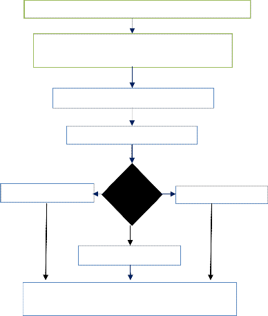
For sample preparation we followed the chart shown below:
Cd (NO3)2.4H2O + Polyvinyl alcohol (PVA)
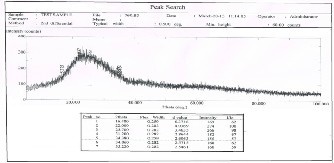
The structure properties of the spin coating CdS films have been investigated by x-ray diffraction technique.Figures1,2, and 3 show the x-ray diffraction patterns at annealing temp.:100Co, 150Co and 200Co
respectively for 20 minutes each. The patterns exhibit peaks at 24.16o, 20.94o and 22.000 respectively, these
Solution(A)
Magnetic stirrer ( T=70 Co, t= 90 min)
Solution A + Thiourea [Cs (NH2)2]
Spin coating
results are comparable to the values obtained by (R. Meshram, 2012) [15] . The presence of small peaks in x- ray diffraction reveals the formation of nano-crystalline
CdS films (also proved by AFM study). The peaks are not sharp indicating that the average crystalline size is small. Due to size effect the peaks in the diffraction broaden and their widths became large as the particles became smaller. The average size of CdS grains has been obtain from x-ray diffraction pattern using equation 1.The values corresponding to each annealing temp. are given in Table 2. It is obvious that the grain size of CdS increases from 29.97 nm to 32.897 nm as the annealing temperature increase from 100C to 200C.
Annealing at 200oC
Thin
films Annealing at 100 C
Annealing at 150 Co
Measurement and studying the optical properties and constants
R.T, then annealed at (100,150,200)Co, then examined by X-ray diffractions using a Philips X-ray diffractometer.
The average size of CdS grains has been obtain from x- ray diffraction pattern use the Scherer's formula
Fig. 1. X-ray diffraction pattern for CdS
at 100Co, 67.66 μm thickness
IJSER © 2013 http://www.ijser.org
International Journal of Scientific & Engineering Research, Volume 4, Issue 12, December-2013 1022
ISSN 2229-5518
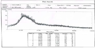
Fig. 2. X-ray diffraction pattern for CdS at 150Co, 67.66 μm
thickness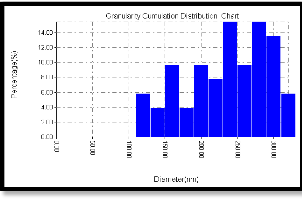
fig. 4 (b)
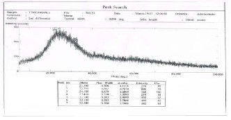
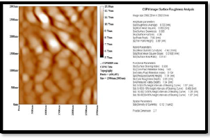
Fig. 3. X-ray diffraction pattern for CdS at 200Co,67.66 μm
thickness
fig. 4 (c)
Figures (4, 5 & 6) show the atomic force microscopic picture for the three samples at different annealing temperature (Ta=100, 150 and 200 ͦC) respectively.
Figures 4( a, b, c, ) show the AFM analysis of the surface of sample annealed at 100 oC ; figure (a) shows a 3D magnified picture of the sample surface
,where we can see the nano-structure of the rough surface. Figure (b) is a panel diagram presents the height profiles measured along the sample surface, it is clear that most particles of (CdS- PVA) are around
250-300 nm with an average diameter of 224.45 nm. As indicaed in figure (c) the average roughness is
0.722nm, this roughness average will be directly changed with increasing the annealing temperature.
Fig. 4. (a) 3D magnified picture of the sample surface ,where we can see the nano-structure of the rough surface.( b) a panel diagram of the height profiles measured along the sample surface, it is clear that most particles are around 250-300 nm . (c) surface roughness analysis.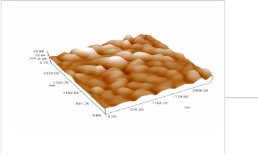
Annealing the sample under 150 oC, the surface shows more obvious structure ,the average particle diameter (CdS- PVA) becomes (212.96 nm) , the crystalline structure of the film is disturbed, resulted in randomly distributed particles we believe that this is due to the melting of sulfur (melting temperature is 131o, rather than the cadmium which has a melting temperature 321oC), also the effect of overcoming the voids and surface defects and rearrangements of the particles. This result is obviously shown in figure (5-a). In figure (5-b) we can see that most of the particles have diameters in the range of (130 -300) nm. Figure (5c) indicates the surface roughness to be 1.21 nm with longer range order.
ER © 2013 www.ijser.org
fig. 4 (a)
International Journal of Scientific & Engineering Research, Volume 4, Issue 12, December-2013 1023
ISSN 2229-5518
surface, it is clear that most particles are around 125-
270 nm . (c) surface roughness analysis.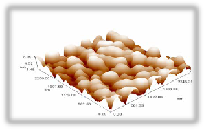
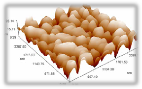
Figure 6(a) shows the annealing under 200 oC which leads to a change in the surface particle distribution giving an average diameter of 156.23 nm., figure 6(b) shows a dramatic change in granularity cumulating distribution, this could be attributed to the particles creep caused by the full melting of PVA and sulfur particles (melting temperature is 131o) and sweeping the Cd particles with them. Figure 6(c) indicates the surface roughness to be 3.5 nm with longer range order.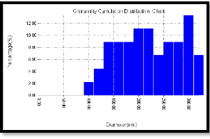
fig. 5 (a)

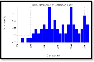
fig. 6 (a)
fig. 5 (b)
fig. 6 (b)
fig. 5 (c)
Fig. 5. (a) 3D magnified picture of the sample surface
,where we can see the nano-structure of the rough surface. (b) a panel diagram of the granularity cumulating distribution measured along the sample
IJSER © 2 http://www.ijs
fig. 6 (c)
International Journal of Scientific & Engineering Research, Volume 4, Issue 12, December-2013 1024
ISSN 2229-5518
Fig. 6 (a) 3D magnified picture of the sample surface ,where we can see the nano structure of the rough surface. (b) a panel diagram of the granularity cumulating distribution of sample surface.. (c) surface roughness analysis.
It is concluded that there is a direct correlation between surface roughness average and annealing temperature. There is also an indirect correlation between the particle size of (CdS- PVA) and annealing temperature.
The absorbance and transmittance spectrum of the samples have been determined by UV- VIS-IR spectrophotometer in the region 300–1100nm. Also the energy gap and optical constants (n, K, α, ε1 , ε2 ) have been determined. Which shows agreement with our result of XRD.
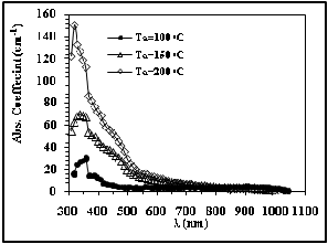
the CdS films is characterized by a strong absorption at the shorter wavelength region between 300–460 nm and without sharp edge on the long wavelength side from 470–530nm.
Fig. 8 Absorption Coefficient versus wavelength
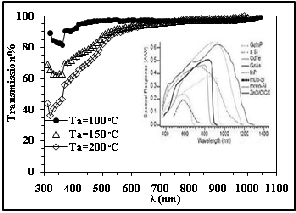
Transmission spectrum
The transmission spectrum for CdS/ PVA thin films
show good transparency (T > 85%). Studying the
silicon response curve, figure 9, we can notice that
IJSEthe response eRxtends from about 400-1000nm, in this
The absorption of CdS thin films are shown in figure 7.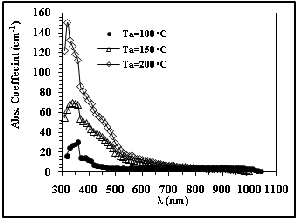
we can notice that the values of absorption increase with increasing the annealing temperature. from the spectra it is evident that the absorption edges are blue shifted with respect to the bulk (520 nm), this result agrees those reported by J.Osuwain, 2009 [16].
Fig. 7. Absorption spectra of CdS/PVA samples, 67.66
μm thickness
The dependence of the absorption coefficient on the wavelength for different annealing temperatures (Ta ) of the deposited CdS films is shown in figure 8; One can see from these figures that the absorption coefficient of
region the studied films show an excellent
transparency. Also it is clear that transmission decrease with increase the annealing temperature as show in Table (3), this could be due to PVA deformation at higher temperature.
Fig. 9 Transmission spectra for CdS/PVA films at different Ta
The optical energy gap values (E g) for CdS films have been determined by using Tauc equation which is used to find the type of the optical transition by plotting the relations of (αhv)2 versus photon energy (hv) and selecting the optimum linear part. The optical energy
IJSER © 2013 http://www.ijser.org
International Journal of Scientific & Engineering Research, Volume 4, Issue 12, December-2013 1025
ISSN 2229-5518
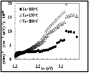
gap decreases with increasing annealing temperature as show in the figures (10). The values are given in Table (2).we find the results are comparable to those obtained by M. S. Tyagi in1991 which is ( 2.42 eV ) [17].
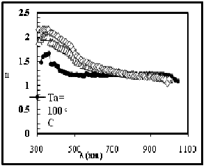
Fig. 11 Refractive index versus wavelength
Fig. 10 Energy Gap for CdS/PVA films with different Ta
Table 2: values of (CdS) grain size at different annealing temp.( obtained from Scherrer's formula) and Energy gap values.
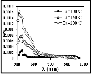
The variation of extinction coefficient with wave length, shown in figure (12). from this figure can note that the extinction coefficient decreased with
increasing the wave length due to high value of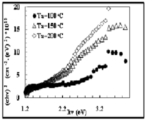
IJSEabsorption coeRfficient. And increase with annealing.
The variation of the refractive index versus wavelength in the range (300–1100) nm, at different annealing temperature (100,150, and 200) 0C is shown in Figure
11. We can notice from these figures and the Table (3) that the refractive index, in general decreases slightly with increasing of Ta.
Fig. 12 The Extinction coefficient versus wavelength
The variation of the real (ε1 ) and imaginary (ε2 ) parts of the dielectric constant values versus wavelength in the range 300-1100 nm at R.T then annealing the films for (100, 150 and 200) oC are shown in Figures ( 13 and 14). The behavior of ε1 is similar to that of the refractive index, while ε2 is mainly depends on the k values, which are related to the variation of absorption coefficient. It is found that ε1 increase with increase the
IJSER © 2013 http://www.ijser.org
International Journal of Scientific & Engineering Research, Volume 4, Issue 12, December-2013 1026
ISSN 2229-5518
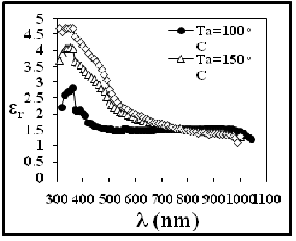
annealing temperatures and ε2 decrease with decrease of annealing temperatures.
annealing temperature. While the transmission of the films are decrease directed with the simple annealing temperature.
The energy gap for CdS thin films decrease due to
increase annealing temperature.
The refractive index and extinction coefficient increase slightly by increasing of annealing temperatures for all samples. The variation of the real and imaginary parts of the dielectric constant have similar trend as for n and k respectively. All results are summarized the table below:
![]()
Grain size 29.9nm 32.58nm 32.9nm
![]()
IJSER
Fig. 13 The Dielectric Constants (Real part)
Absorption
of films
0.011 0.028 0.035
Transmissio n spectra
97.427
%
93.691% 92.235
%
![]()
![]()
![]()
Optical Energy Gap Absorption Coefficient Refractive Index
2.25 1.65 1.60
3.854 9.634 11.949
1.217 1.359 1.405
Extinction
Coefficient
1.84*10
-5
4.60*10-5 5.71*10-
5
Dielectric
Constants
εr 1.48
2
1.84
8
1.974
Fig. 14 The Dielectric Loss (imaginary part) Table 3:optical constants at λ =600 nm conclusion
In summery the CdS embedded in PVA matrix in thin films was prepare using spin coating technique. The effect of annealing on prepare films at thickness about
67.66 μm were. From the x-ray diffraction the crystal
grain size increase with increase the annealing temperature .The absorption of the films and the absorption coefficient increase with increases the![]()
εi
*10-5
4.48 12.5
1
16.04
IJSER © 2013 http://www.ijser.org
International Journal of Scientific & Engineering Research, Volume 4, Issue 12, December-2013 1027
ISSN 2229-5518
16- J.Osuwain ,chalcogenide letters vol. 6, no. 9, sep.2009, p. 433-436
17- M. S. Tyagi. " Introduction to Semiconductor
Material and Devices ". John Wiley and Sons, Canada 1991.
1- B. Saporal, and C. Hermann "physics of Semiconductors" Springer-Verlag, New York, Inc., (1995)
2- H. Bach and D. Krause "thin films on Glass" Springer-Verlag Berlin
3- A.K. Abass "Solar Energy Material" (1988)
4- C. Kittle "Introduction to Solid State Physics" Eight Edition, John Wiley and Sons, p.416,(2005).
5- S.M.Sze "Physics of Semiconductor Devices" John Wiley and Sons,(1981).
6- B.L.Sharma, R.K.Purohit and S.N.Mukerjee "Infrared Physics", Vol.10, pp.225-231, Pergamon Press, printed in Great Britain, (1970).
7- A.G.Milnes and D.L.Feucht, "Heterojunctions and Metal-Semiconductor Junctions", Academic Press, New York and London (1972).
8- K. Hu, M. Brust and A. Bard, Chem. Mater. 10 (1998) 1160.
9- H. Weller, Angew. Chem., Int. Ed. Engl. 32
(1993) 41.
10- M. S. Tyagi. " Introduction to Semiconductor Material and Devices ". John Wiley and Sons, Canada 1991.
11- N.Wenstem, G.M. Wolf and B.N. Das. Appli.
Phys. Let. ,6:73 ,1965.
12- D. A. Cusano. Solid State Electron. 6:217, 1963
13- G.Mandel. Phy. Rev. ,134:A1073 ,1964
14- H. Chavez, M. Jordan , J. C. Mc Clure, G. Lush and V. P. Singh. J. Mater. Sci. Mater . Electron.
8:151, 1997
15- R. Meshram, advances in applied science
research,2012,3(3),1563-1571
IJSER © 2013 http://www.ijser.org