International Journal of Scientific & Engineering Research, Volume 2, Issue 11, November-2011 1
ISSN 2229-5518
Effect of Adding Input and Output Impedance Transformer on Wilkinson Power Dividers Performance
A. Al-Hindawi, S. Mahmood
Abstract— Even though the two-stage Wilkinson N-way power divider is simple to design, realize and test, It has been used with strict restrictions in design and fabrication because it requires a very high impedance microstrip line, i.e., extremely low aspect ratio W/H or very thin line conductor width. To overcome this limitation in realizable characteristic impedance a quarter-wave length impedance transformer section between two lines is used. This research investigates the effect of adding quarter-wave lines impedance transformation to two- stage Wilkinson N-way power divider on the performance parameters.
Index Terms—Wilkinson, N-way, impedance transformer, Quarter-wave impedance transformer, Microstrip, power divider, combiner.
—————————— ——————————
1 INTRODUCTION
OWER dividers and combiners are used widly in RF/microwave power amplifiers, linearizers, and many kinds of test equipments. Among many sorts of divider,
the Wilkinson topology shows the basic concept of N-way power dividing by its simple structure. The two-stage Wilkin- son N-way power divider is a typical application of the Wil- kinson structure, because it is simple and easy to design, real-
ize, and test [1],[2]. On the contrary to this simplicity of the
able ranges of strip width in the construction of a specific cir- cuit.
The most convenient way of doing this is with the single or multi-section quarter-wave stepped impedance transformer. In its simplest form for narrow band operation, this consists of a quarter-wave section whose impedance is the square root of the ratio of the impedance transformation.
divider, the two-stage Wilkinson N-way power divider has been used with strict restrictions in design and fabrication be-
ZB =

ZA ZC
(1)
cause it requires a microstrip line with very high impedance, i.e., very low aspect ratio W/H (ratio of line width W to the substrate thickness H) or very thin conductor width. For ex- ample, a four-way Wilkinson divider requires 141Ω microstrip line. In practice, the characteristic impedance of a realizable microstrip has its limitation at around 135Ω - 145Ω, although it depends on the dielectric constant (εr) and the thickness of the substrate. It is almost impractical to realize a 141Ω line using the conventional microstrip structure [3],[4]. To overcome this limitation in realizable characteristic impedance a quarter- wave impedance transformer section between two lines was added to the N-way power divider design, which gives a width to the microstrip line conducter than that is required for the same characteristic impedance
2 ANALSIS
2.1 Quarter Wave Impedance Transformere
There are many occasions when it is desirable to transform the impedance of a line from its fundamental impedance to either a higher or lower impedance amount, either for use as a pow- er divider or combiner, or to enhance the aspect ratio of com- ponents which are constructed at the higher frequencies. Be- cause of the limited range of impedances available with mi- crostrip construction (20-145) ohms [2],[3], it is also frequently necessary to transpose impedance in order to provide reason-
[ZB] is the additional impedance transformer line, [ZC] is im- pedance required to be transformed to, [ZA] is impedance to be transformed as shown in Fig. 1.
Fig.1 matching transformation lines (transforming A to line C by B)
[ZC] can be a point at the end of the line [B] that will be con- nected directly to the connecter as shown clearly in Fig.2.[2]
Fig.2 matching transformation lines (transforming A to point C by B)
2.2 Microstrip Power Divider Design
The Wilkinson N-way power divider / combiner was presented by Adel A. M. Saleh [5], in this research we were concerned in the two stage fork N-way power divider. Fig. 3 shows the repre- sentation of the two-stage power divider; R1 and R2 are the isola- tion resistors, Zc is the
input impedance, Zd is the output impedance. The values of the
design line impedances are calculated by:
IJSER © 2011
http://www.ijser.org
International Journal of Scientific & Engineering Research, Volume 2, Issue 11, November-2011 2
ISSN 2229-5518
Zo,1 (NZc
)3 / 4 (Z
)1 / 4
(2)
A two stage three way power divider is designed on a
RT/Duroid 3010 with 10.2 dielectric constant, 0.0035 dissipa-
Zo,2 (NZc
)1 / 4 (Z
)31/ 4
(3)
tion factor and 1.25 mm thickness ,with 50 ohms input and out
puts impedance, a
g / 4
line at mid band frequency of 2.25
Where Zo,1 and Zo,2 are the line impedances of the first and
second stage in the two-stage power divider respectively and N is the number of divisions of the power divider, as shown in Fig.3.
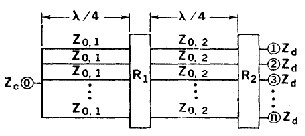
Fig.3 Representation of two-stage Power Divider
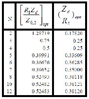
Table-1 shows the values of the optimum match and isolation resistors R1 and R2 for the two-stage fork N-way power di- vider with divisions 2-12 [5].
TABLE 1
VALUES OF ISOLATION RESISTORS FOR TWO-STAGE N-WAY POWER
DIVIDER
2.3 Design and Implementation of Three-Way Two
Stage Power Divider
Table-2 shows the design impedances of the 2 to 12 way two stage power divider (Trans 1) is the quarter-wave impedance transform line added to the input impedance Zin and (Trans 2) is the quarter-wave impedance transform line added to the output impedance Zout. As can be seen from the table that having a 50Ω input and output impedance is limited to the two, three and four way two stage power divider only and if thinking to build a five till twelve ways a quarter-wave im- pedance transformer line has to be added either at the input or output or both ports as demanded in the nine, ten, eleven and twelve ways two stage power divider.
GHz is 1.10 mm wide and 12.71 mm in length. The two stage three way power divider designed by Using equations (2) and (3), had the impedance values
Zin Zout 50
Z0,1 113
Z0, 2 65
TABLE 2
THE DESIGN IMPEDANCES AND TRANSFORMATION IMPEDANCES FOR TWO STAGE POWER DIVIDERS
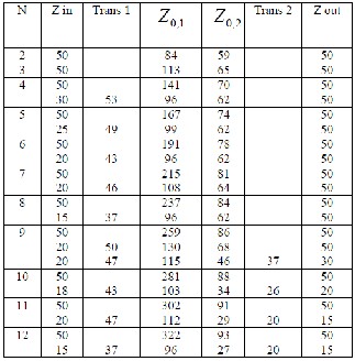
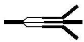
Fig.4 shows the layout of the design and fig. 5 show the pho- tograph of the fabricated divider.
Figure .4 Layout of three-way two-stage power divider on RT/ Duroid 3010 substrate (Dim100mmX45mm)
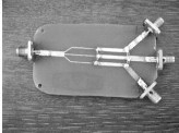
Figure.5 Photograph of three-way two-stage power divider on RT/ Duroid
3010 substrate (Dim100mmX45mm)
IJSER © 2011
http://www.ijser.org
International Journal of Scientific & Engineering Research, Volume 2, Issue 11, November-2011 3
ISSN 2229-5518
The previous design will be compared to another three way two-stage power divider fabricated also on RT/Duroid 3010 substrate but having the quarter-wave impedance transform lines added to the input and the outputs to investigate the ef- fect of the addition
The values of the design impedances by using equations (2)
and (3) are
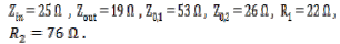
The additional transformation matching lines calculated using equation (1) are added, {B}=35 Ω is inserted in the design to transform the impedance {A}= 25 Ω to {C}= 50 Ω. Also an ad- ditional 30 Ω stub is inserted to transform 19 Ω output to the
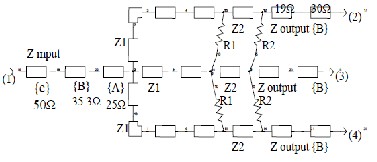
50 Ω line as shown in fig. 6, [6].
Figure.6 Schematic diagram of three-way two-stage power divider with input and output quarter line transformations
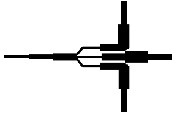
Figure.7 Layout of three-way two-stage power divider on RT/ Duroid 3010 substrate (Dim110mmX60mm)
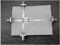
Figure.8 Layout of three-way two-stage power divider on RT/ Duroid 3010 substrate (Dim110mmX60mm)
3 RESULTS OF SIMULATION AND MEASURMENTS
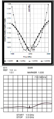
The two fabricated dividers are analyzed and simulated by Genesys software [7] and their characteristics measured by the network analyzer 8510 HP. The main disadvantage of using the transformation lines is the narrow bandwidth of the over- all performance of the circuit as related to a circuit with no transformation lines used and the additional length of the cir- cuit that leads to more insertion loss. Figures 9, 10, 11, are the response curves of the three-way two-stage power divider with no transformation lines used, the (a) figures are the simu- lated outputs and the (b), (c), and (d) figures are the measured outputs. Figures 12, 13, 14, are the response curves of the three-way two-stage power divider with the transformation lines added (a) are the simulated curves while (b), (c), and (d) figures are the measured responses.
Fig 9 (a)
Fig 9 (b)
Fig 9 (c) 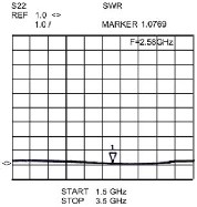
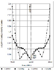
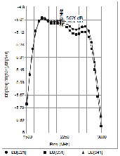
Figure.9 Response curves for three-way two-stage power divider designed on a Duroid 3010 substrate, (a) simulated input VSWR1 and simulated output VSWR2, VSWR3, VSWR4 (b) measured input VSWR, (c) meas- ured output VSW
IJSER © 2011
http://www.ijser.org
International Journal of Scientific & Engineering Research, Volume 2, Issue 11, November-2011 4
ISSN 2229-5518
Fig 10 (a)
Fig 10 (b) 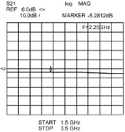
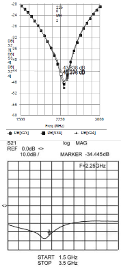
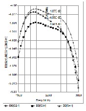
Figure. 10 Response curves for three-way double stage power divider designed on a Duroid 3010 substrate. (a) Simulated coupling (b) meas- ured coupling
Fig 11 (a)
Fig 11 (b)
Figure.11 Response for three way double stage power divider designed on a Duroid 3010 substrate, (a) Simulated isolation (b) Measured isolation
Fig 12 (a)
Fig 12 (b) 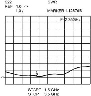
Fig 12 (c) 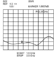
Fig 12 (d) 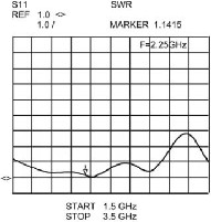
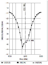
Figure. 12 Response curves for three-way two-stage power divider de- signed on a Duroid 3010 substrate (a) Simulated output and input VSWR (b), (c) and (d) measured VSWR
IJSER © 2011
http://www.ijser.org
International Journal of Scientific & Engineering Research, Volume 2, Issue 11, November-2011 5
ISSN 2229-5518
Fig 14 (a)
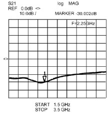
Fig 13 (a)
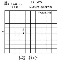
Fig 14 (b)
Fig 13 (b)
Fig 13 (c) 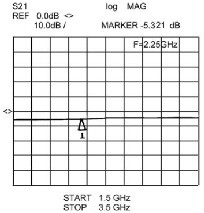
Figure. 13 Response curves for three way double stage power divider designed on a Duroid 3010 substrate, (a) Simulated coupling (b), (c) Measured coupling
Figure. 14 Response curves for three way double stage power divider designed on a Duroid 3010 substrate, (a) Simulated isolation (b) Meas- ured isolation
4 DISCUSSION
Comparing the previous simulated and measured curves for both the two stage three way power divider with and without quarter transformation lines it can be concluded that the main parameter effected was the insertion loss due to the additional lines added in the case of adding the quarter wave transforma- tion lines, and the other parameter changed was the band- width that was less in the case of adding the quarter wave transformer lines to the power divider.
5 CONCLUSIONS
Adding the quarter wave transformation lines was a simple and cheap way to overcome the difficulties and limitation of fabricating N way power dividers which has high impedance related to high number of division. The effects of transforma- tion lines on two-stage Wilkinson N-way power dividers were studied. Two-stage Wilkinson two to twelve way power di- vider was analyzed. Two prototype of three way two-stage power divider were designed, implemented and tested. The results of simulation and measurements were plotted and dis- cussed. Mainly bandwidth and insertion loss were affected negatively when adding transformation lines as was shown in the simulated and measured results.
IJSER © 2011
http://www.ijser.org
International Journal of Scientific & Engineering Research, Volume 2, Issue 11, November-2011 6
ISSN 2229-5518
6 REFERENCES
[1] S. Shamsinejad, M. Soleimani and N. Komjani, “Noval Miniatu- rized Wilkinson Power Divider for 3G Mobile Receivers”, Progress In Electromagnetics Research Letters, Vol.3, pp 9-16,
2008.
[2] Bharathi Bhat, Shiban K. Koul,” Stripline-like transmission lines for microwave integrated circuits”, New Age International, 1989
[3] Howe,Harlan, Stripline circuite design, Artech House, 1974
[4] Wilikinson. E.J., “An N-way Hybrib power divider”, IEEE Trans.Microwave Theory Thech., Vol. 13MTT-8 ,No.1, pp.116-
118, Jan. 1960
[5] Adel. A. M. Saleh, “Planer Electrically Symmetric N-Way Hybr- id Power Dividers/ Combiners”, IEEE Trans. Microwave Theory Tech., Vol. MTT-28, No.6, June 1980.
[6] S.M. Al-Ali, A. M. Al-Hindawi, “Effects of transformation lines on two-stage Wilkinson N-way power divider,” The 2005 Inter- national Conference on Computer & Power, Feb.14-16, Saltanat Uman, 2005
[7] Eagleware Corporatio, Genesys V.7 eagleware RF & Microwave
Design Softwre, 1999
IJSER © 2011
http://www.ijser.org