International Journal of Scientific & Engineering Research, Volume 4, Issue 7, July-2013 119
ISSN 2229-5518
Dvts Apporach to Digital Cmos Circuits for
Decreasing Total Power Consumption
Archanadevi.C, Vishnu Vardhan Rao.G,
Abstract— Power consumption of Modern Digital integrated circuits increasing with each generation which becomes a serious design issue. This paper proposed a generalized power tracking algorithm that reduces power directly by dynamic control of supply voltage and body bias. The DVTS algo-rithm-(Dynamic Voltage and threshold scaling algorithm) save the leakage power during active mode of the cir- cuit.Total active power can be minimized by dynamically adjusting Vdd and Vth based on circuit operating conditions such as temperature, workload, and circuit architecture. The power saving method of DVTS is similar to that of the Dy-namic VDD Scaling (DVS) scheme, which adaptively changes the supply voltage depending on the current work-load of the system. For a digital circuit, it is possible to trade off dynamic and sub threshold leakage power by balancing between Vdd and Vth to maintain performance.
Index Terms— Dynamic voltage and threshold scaling (DVTS), leakage current control, low power, power optimum point, sleep transistor, variable body bias, and variable supply voltage.
1 INTRODUCTION
—————————— ——————————
Low power has emerged as a principal theme in to- day’s electronics industry. The need for low power has caused a major paradigm shift where power dissipation has become as important a consideration as performance and area. In the past, the major concerns of the VLSI designer were area, perfor- mance, cost and reliability; power consider-ation was mostly of only secondary importance. In recent years, however, this has begun to change and, increasingly, power is being given com- parable weight to area and speed considerations. Several factors have contributed to this trend. Perhaps the primary driving factor has been the remarkable success and growth of the class of personal computing devices (portable desktops, audio- and video-based multimedia products) and wireless communica- tions systems (personal digital assistants and personal commu- nicators) which demand high-speed computation and complex functionality with low power consumption
.
Power dissipation has become an important objective
in the design of digital circuits. There has been intense re-
search over the past two decades on various aspects of compi-
lation and synthesis for low power. Many architectural opti-
mizations like re-configurable architectures, custom ASIC ap-
proaches, programmable multi-cores, etc. have been explored. Micro-architectural techniques like parallelism and pipelining, power and clock gating have become common place now. Cir- cuit techniques for low voltage operation, standby current
reduction, optimal gate sizing have also been explored and are available for use by a designer. Most of these optimization techniques are static techniques which are applied during de- sign time. In the recent past, dynamic power management techniques have emerged, where the power consumption is continuously adjusted during run time of the system. Traditionally, Dynamic power management (DPM) is em- ployed at operating system level to adjust the supply voltage for each power state. The supply voltage is conservatively margined to account for process and temperature variations.
These voltage margin increases with technology scaling due to larger process variations, rendering DPM less efficient. On the other hand, the hardware approach like dynamic voltage scal- ing (DVS) allows voltage to be scaled such that the actual de- lay of the chip instead of worst case delay meets the target performance. This enables more power savings as minimum possible voltage for target performance can be attained. In DVS the supply voltage is adjusted to meet the target delay using an on-chip delay monitor in a hardware feedback loop. Performance degradation is a direct consequence of supply voltage reduction. In order to maintain the required through- out, dynamic voltage scaling (DVS) systems are used to adjust the supply voltage according to throughput requirements. Though DVS very well manages the dynamic switching pow- er, with shrinking feature size the static (leakage) power has increased exponentially which it cannot control. Particularly, at low activity levels, leakage power is dominant.
We present a Dynamic VTH Scaling (DVTS) scheme to save the leakage power during active mode of the circuit. Dynamic voltage and threshold scaling (DVTS) manages both dynamic and leakage powers by adjusting supply voltage and body bias voltage. The power saving strategy of DVTS is simi- lar to that of the Dynamic VDD Scaling (DVS) scheme, which adaptively changes the supply voltage depending on the cur- rent workload of the system. Instead of adjusting the supply voltage, DVTS controls the threshold voltage by means of body bias control, in order to reduce the leakage power. The power saving potential of DVTS and its impact on dynamic and leakage power is applied to future technologies.
2 DYNAMIC VOLTAGE AND THRESHOLD SCALING
Dynamic voltage and threshold scaling (DVTS) man- ages both dynamic and leakage powers by adjusting supply voltage and body bias voltage In digital circuits de-signed be- low 0.1 m, total power at any given performance can be opti-
IJSER © 2013 http://www.ijser.org
International Journal of Scientific & Engineering Research, Volume 4, Issue 7, July-2013 120
ISSN 2229-5518
mized by DVTS. DVTS has been successfully proven on silicon for low power high speed applications. The optimum power point varies strongly with activity and temperature.DVTS of- fers considerable power savings com-pared to DVS when leakage power is a large fraction of total power. The power savings increase with increasing logic depth. The moderate performance application-specific inte-grated circuit (ASIC) with long logic depth at low activity and/or high tempera- tures gain the most with DVTS.
2.1 Overview of Dvts
Dynamic VTH Scaling (DVTS) scheme for active leakage power reduction. Whenever there is a slack during computation, the VTH is adaptively changed to a higher value via changing the body bias voltage (VBB). This will deliver just enough amount of throughput required for the current workload. In order to examine the effectiveness of DVTS, comparisons between DVS and DVTS for current (0.25μm) and future (0.07μm) process generations are performed. A careful investigation on the advantages and disadvantages of DVTS over DVS is also made. A DVTS hardware that has a feedback loop consisting of a voltage controlled oscillator (VCO), charge pumps a feedback controller is proposed. The clock frequency of the system for a certain workload is deter- mined by the operating system in run-time. The DVTS hard- ware tracks the optimal VTH for the given clock frequency by dynami-cally adjusting the VBB.
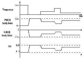
“Fig.1.Dynamic VTH scaling by adaptively changing the body bias”.
Fig.1 shows how the DVTS scheme adaptively controls the body bias to change the VTH. For a time period when the workload is less than the maximum, the operating system will recommend a lower clock frequency to the hard- ware. Then the DVTS hardware will increase the PMOS body bias and decrease the NMOS body bias to raise the VTH and reduce power dissipation. In cases when there is no workload at all, the VTH can be increased as much as the upper limit of VBB, to significantly save the standby leakage power. Reduc- ing the clock frequency will proportionally reduce the total power. However, simply reducing the clock rate does not af- fect the energy consumed per operation. Whereas by scaling the supply voltage together with the frequency, we can gain
significant power savings. This is because the dynamic power dominates the total power. Scaling the threshold voltage in- stead of scaling the supply voltage saves mostly the leakage power. For 0.25μm technology where the leakage power is a minute portion of the total power, DVTS is less efficient than DVS in saving total power..
2.2 Modules of Dvts
2.2.1 VDD Controller
• Vdd is the power supply to the digital circuit. Vdd will be scaled according to power consumption and time delay Maximum time delay will be set and be- tween in that limits Vdd will be scaled.
• If Vdd goes below the minimum Vdd value Vdd val ue will be increased.
2.2.1 VBS Controller
• Vbs is the voltage between source and substrate. Vbs will effect threshold voltage .Vbs of the digital circuit will be varied to decrease the threshold voltage.
• In DVS only Vdd will be scaled to decrease total pow- er consumption in dvts approach both Vdd and Vbs will be scaled to decrease total power consumption.
2.3 DVTS Scheme
Dynamic VTH Scaling (DVTS) scheme for active leakage power reduction. Whenever there is a slack during computation, the VTH is adaptively changed to a higher value via changing the body bias voltage (VBB). This will deliver just enough amount of throughput required for the current workload. In order to examine the effectiveness of DVTS, comparisons between DVS and DVTS for current (0.25μm) and future (0.07μm) process generations are performed. A careful investigation on the advantages and disadvantages of DVTS over DVS is also made. A DVTS hardware that has a feedback loop consisting of a voltage controlled oscillator (VCO), charge pumps a feedback controller is proposed. The clock frequency of the system for a certain workload is deter- mined by the operating system in run-time. The DVTS hard- ware tracks the optimal VTH for the given clock frequency by dynamically adjusting the VBB.
2.4 Dvts Controller
Fig.2 shows block diagram of close loop DVTS sys- tem. DVTS controller implements the proposed DVTS algo- rithm and controls the supply voltage regulator and well bias charge pump. Control signal generator (CSG) generates con-
IJSER © 2013 http://www.ijser.org
International Journal of Scientific & Engineering Research, Volume 4, Issue 7, July-2013 121
ISSN 2229-5518
trol signals for power monitor when START signal is asserted. The proposed DVTS system is suited for load circuits where the rate of change in activity is gradual. DVTS controller imple- ments the proposed. DVTS algorithm and controls the supply voltage regulator and well bias charge pump. The drain of sleep transistor acts as a virtual ground node for the load circuit.
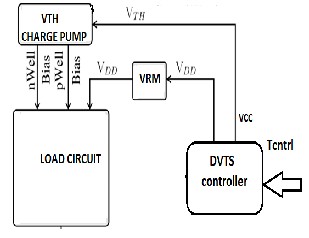
“Fig.2 Design Implementation Block Diagram”
The power monitor processes virtual ground voltage to generate a 2 bit output that gives information on total pow- er consumed by the load. Control signal generator (CSG) gen- erates control signals for power monitor when START signal is asserted. The delay monitor measures whether performance of load circuit meets the target performance within tolerance lim- it. Delay monitor is implemented with a critical path replica circuit. The proposed DVTS system is suited for load circuits where the rate of change in activity is gradual. The maximum rate of change of activity that can be supported is discussed.
3 DVTS ALGORITHM
Fig.3.1 shows the flow chart of the proposed DVTS algo- rithm. The algorithm first sets the supply voltage to meet target per- formance, then adjust well potential to achieve minimum power. NWell bias and P Well bias are always tuned by same amount and hence DVTS control loop is essentially a 2-D control loop. To avoid oscillations, loop and loop are decoupled by tuning them inde- pendently. Initially maximum supply voltages and maximum forward bias are applied and the supply voltages are slowly lowered. At each step, the body bias is reset to maximum for- ward bias and locks to the target frequency to ensure that the chip stays functional. Once the minimum power point is de- tected, the bias values can be held in a register and the control- ler turned off. The loop can be reactivated whenever the work- load changes, or periodically updated to reflect changes in
temperature or operating conditions. Because the ASB loop does not have to be constantly running, the overhead power consumption, which is already amortized across the whole chip, can be reduced even further. This ASB control loop is
completely self-contained and should lock to the true mini- mum power configuration taking into account all possible current paths
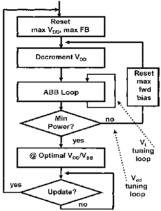
“Fig.3 (a) Flowchart for automatic Vdd /Vth optimization.”
This minimum will result in the physically lowest power consumption achievable by tweaking both and subject to the constraint that the chips satisfy a target frequency. Even for technologies where the theoretical limit is not yet achieva- ble using body biasing techniques or in cases where excessive forward bias at low degrades performance, it is still possible to use this architecture to find the minimum physical power condition. The threshold voltage can be controlled by chang- ing the body bias of the transistors and is called the adaptive body bias (ABB) technique. For fast silicon, reverse body bias is applied to increase threshold and reduce leakage, while for slow silicon, forward body bias is applied to reduce threshold and improve performance. Here the body bias adjustment is done sparingly as needed based on the chip’s process condi- tion, and is not a continuous variable like the supply voltage. However the point of minimum power depends on the ratio of dy- namic to leakage power, with the former modulated by the activity factor. For media applications, the activity factor can vary a lot across differ-ent applications and hence, the optimal settings for threshold and supply also vary .Analogous to table based DVS, a table based DVTS scheme has been proposed where for different activity factors, the corresponding supply and body bias values are stored in the look up table. The activity factors
IJSER © 2013 http://www.ijser.org
International Journal of Scientific & Engineering Research, Volume 4, Issue 7, July-2013 122
ISSN 2229-5518
are estimated for different applications off-line. During run-
time, based on the application being run, the appropriate ac-
tivity factor is used to consult the look up table to obtain the
settings for supply and body bias, which will minimize power.
Adaptive voltage and threshold scaling aims to arrive at the
optimal voltage and threshold values at run time, by not only
adapting to the process and temperature like in AVS, but also
to the dynamically varying activity conditions.
4 ADVANTAGES DVTS OVER DVS
No voltage level converters:
DVS or multiple VDD systems require a voltage level shifter whenever a low VDD signal is driving a high VDD receiver. Although the conventional level converters prevent the static power consumption, the dynamic power consumption is large enough to cancel out the power savings gained from supply voltage scaling. Since DVTS systems use the same supply voltage throughout the chip, no voltage level converters are required.
Simple hardware:
Charge pumps are a simple solution for boosting voltages. No external inductors are needed and power con- sumption is very low compared to buck converters, which are used for DVS systems. Charge pumps are used for our DVTS system to generate the body bias voltages
Less power loss charging/discharging internal nodes:
Transition energy wasted charging/discharging the VDD ground capacitance is the power overhead of the DVS scheme. For low-to-high and high-to-low transition of supply voltage, current is extracted or placed back to the power supply. Even though there is no computation during this cy- cle, transition energy is consumed. Since the supply voltage is fixed for DVTS, it has less transition energy loss while charg- ing and discharging the internal nodes.
Improvement in noise immunity:
Signal integrity has become an important issue for deep sub micron devices as crosstalk noise becomes consider- able. Increasing VTH for low workload periods in DVTS will help improve noise immunity, especially for noise-susceptible circuits such as domino logic and pulsed flip-flops.
5 RESULTS AND DISCUSSION
To mitigate the active leakage problem, a Dynamic VTH Scaling (DVTS) scheme is presented. DVTS algorithm that can be studied and implemented for the design of VDD controller. VDD will be scaled and controlled according to the limits for the circuit. Power reduction technique can be ap- plied to basic cmos circuits and the results for average power are analyzed. Ex. Inverter, NAND, NOR, multiplexer this idea can be extended to larger circuits in future
5.1 VDS and VBS controller results
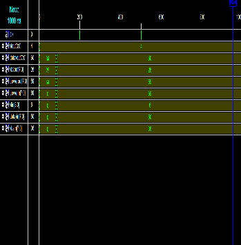
“Fig.5.1 VDD controller Graph results”
“Fig 5.2 VBS controller Graph results”
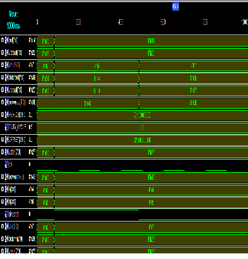
6 DVTS CONTROLLER RESULTS
IJSER © 2013 http://www.ijser.org
International Journal of Scientific & Engineering Research, Volume 4, Issue 7, July-2013 123
ISSN 2229-5518
.
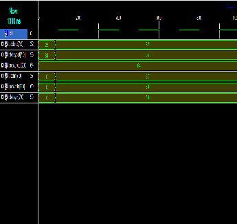
“Fig 6.1 DVTS controller Graph results”
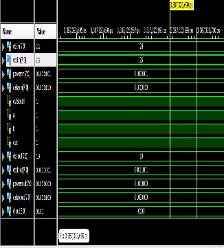
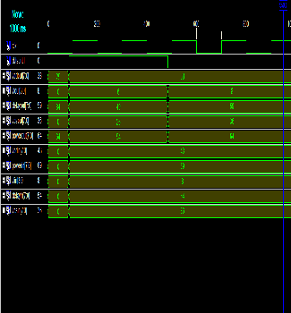
“Fig 6.2 One Bit Multiplier Graph results”
“Fig 6.3 Four Bit Multiplier Graph results”
7 Appendices
IJSER © 2013 http://www.ijser.org
International Journal of Scientific & Engineering Research, Volume 4, Issue 7, July-2013 124
power consumption by means of supply and threshold voltage con- trol in ac-tive and standby modes,” IEEE J. Solid-State Circuits
[8] Wang and A. Chandrakasan, “Optimal supply and threshold scaling for subthreshold CMOS circuits”in proc, IEEE Comput. Soc. An- nu.Symp. VLSI, 2002, pp. 5–9.
————————————————
• Archanadevi.c is currently pursuing masters degree program in vlsi design in VelTech Multitech Dr.Rangrajan Dr Sakunthala engineering college, AnnaUniversity, Chennai, India, PH-9600876743. E-mail: ar- chujc@gmail.com.
• Mr.G.Vishnu Vardhan Rao is currently working as Asstitant professor in VelTech Multitech Dr.Rangrajan Dr Sakunthala engineering college, AnnaUniversity, Chennai, India,, PH-9566157408. E-mail: gaudipudir
@gmail.com.
(This information is optional; change it according to your need.)
ACKNOWLEDGMENT
The authors are thankful to IJSER Journal for the support to develop this document.
REFERENCES
[1] J. Kao, M. Miyazaki, and A. Chandrakasan, “A 175- MV multiply- accumulate unit using an adaptive supply voltage and body bias ar- chitecture,” IEEE J. Solid- State Circuits, vol.37, no.11,Nov.2002.
[2] K. Nose and T. Sakurai, “Optimization of VDD and VTH for low power and high speed applications,” in Proc. Asia South Pacific Des. Autom. Conf., 2000, pp. 469–474.
[3] M. Elgebaly and M. Sachdev, “Variation-aware adaptive voltage
scaling system,” IEEE Trans Large Scale Integr. (VLSI) Syst., vol. 15, no. 5, pp 560–571, May 2007.
[4] ] R. McGowan, C. Poirier, C. Bostak, J. Ignowski, M. Millican, W.
Parks, and S. Naffziger “Power and temperature control on a 90-nm Itanium family processor,” IEEE J. Solid-State Circuits, vol. 41, no. 1, pp. 229–237, Jan. 2006
[5] T. Burd, T. Pering, A. Stratakos, and R. Brodersen, “A Dynamic volt- age scaled microprocessor system,” IEEE J. Solid-State Circuits, vol.35, no. 11, pp. 1571–1580, Nov. 2000.
[6] T. Kuroda, K. Suzuki, S. Mita, T. Fujita, F. Yamane, F. Sano, A. Chiba, Y. Watanabe, K. Matsuda, T. Maeda, T. Sakurai, and T. Furuyama, “Variable supply-voltage scheme for low-power high-speed CMOS digital design,” IEEE J. Solid-State Circuits, vol. 33, no. 3, pp. 454–
462, Mar. 1998,
[7] U. Nomura, Y. Ikenaga, K. Takeda, Y. Nakazawa, Y. Aimoto, and
Y.Hagihara“Delay and power monitor-ing schemes for minimizing
IJSER © 2013 http://www.ijser.org