International Journal of Scientific & Engineering Research, Volume 2, Issue 2, February-2011 1
ISSN 2229-5518
Design of Low-Power CMOS Cell Structures
Using Subthreshold Conduction Region
Vishal Sharma, Sanjay Kumar
Abstract— Subthreshold (leakage or cut-off) currents are a necessary evil in traditional VLSI design methodologies. These currents increase exponentially as threshold voltage scales, creating a serious problem for traditional design approaches. This work is based on the exclusive use of subthreshold conduction currents to perform circuit operations, turning this problem into an opportunity. It yields a dramatic improvement in power consumption compared to traditional circuit design approaches. This improvement makes it feasible to design extreme low-power circuits with such an approach. The CMOS digital circuits for this work have been designed using standard TSMC 0.18 1-m Technology.
Index Terms—Low-Power, Leakage Current, Subthreshold Conduction.
—————————— • ——————————
With the growing scale of integration, more and more sophisticated signal processing systems need to be im- plemented on a VLSI chip. For these signal processing applications, power consumption has become a critical concern in today’s VLSI system design. The need for low- power VLSI systems arises from two main forces. First, with the steady growth of processing capacity per chip, large current has to be delivered and the heat due to large power consumption must be removed by proper cooling techniques. Second, battery life in portable electronic de- vices is limited. Low-power design directly leads to pro- longed operation time in these portable devices.
Also, with shrinking technology sizes, energy effi- ciency has become a critical aspect of designing digital circuits. Traditionally, voltage scaling, a mechanism in which the supply voltage is varying and the threshold voltage is constant, has been an effective solution in meet- ing stringent energy requirements. However, voltage scal- ing does come at a cost of reduction in performance. The limits of voltage scaling, and therefore energy minimiza- tion, can be explored by operating a circuit at subthresh- old [1]. In subthreshold circuits, the supply voltage is re- duced well below the threshold voltage of a transistor. Due to the quadratic reduction in power with respect to the supply voltage, subthreshold circuits are classified as ultra low-power circuits.
Specifically in application areas where performance
can be sacrificed for low-power, subthreshold circuits are an ideal fit. Some of the applications include devices such as digital wrist watches, radio frequency identification (RFID), sensor nodes, pacemakers and battery operated
————————————————
• Vishal Sharma is with the Electronics and Communication Engineering
Department, ICFAI University, Dehradun, India.
• Sanjay Kumar is with the Electronics and Communication Engineering
Department, Thapar University, Patiala, India.
devices such as, cellular phones.
Up until now, the power consumption has not been of great concern because of the availability of large packages and other cooling techniques having the capability of dis- sipating the generated heat. However, continuously in- creasing density as well as the size of the chips and sys- tems might cause to difficulty in providing adequate cool- ing and hence, might either add significant cost to the system or provide a limit on the amount of the functional- ity that can be provided [2].
Another factor that fuels the need for low-power chips
is the increased market demand for portable consumer electronics powered by batteries. For these high perform- ance portable digital systems, running on batteries such as-laptops, cellular phones and personal digital assistants (PDAs), low-power consumption is a prime concern be- cause it directly affects the performance by having effects on battery longevity.
Hence, low-power VLSI design has assumed great im- portance as an active and rapidly developing field. Due to their extreme low-power consumption, subthrehsold de- sign approaches are appealing for a widening class of applications which demand low-power consumption and can tolerate larger circuit delays.
In traditional digital VLSI design, the subthreshold re- gion of operation is avoided, since it contributes toward leakage power consumption when the device is in stand- by. But the power can be reduced significantly by exclu- sively utilizing this subthreshold leakage current to im-
plement circuits. This is achieved by actually setting the
IJSER © 2010 http://www.ijser.org
International Journal of Scientific & Engineering Research, Volume 2, Issue 2, February-2011 2
ISSN 2229-5518
circuit power supply Vdd to a value less than or equal to
is the effective mobility, Cox is the oxide capacitance, n
Vth . The subthreshold current is exponentially related to
![]()
is the subthreshold slope factor n = 1+ , Vth
is the
gate voltage giving the exponential reduction in power consumption, but also an increase in circuit delay [3]. So, we use the circuits operating in subthreshold conduction region where the power is main concern and large delay can be tolerated.
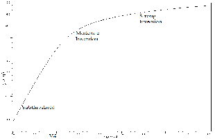
The MOS transistor conducting below the threshold
voltage Vth is called subthreshold conduction. Fig. 1 shows that the current Id has linear dependency in the
strong inversion region while in the moderate inversion
region it shows quadratic dependency on gate voltage. The current in subthreshold conduction region changes exponentially, similar to BJT operation.
Cox
transistor threshold voltage and VT is the thermal volt-
age,VT =( kT/q).
In this section, we will discuss a closed form solution
for the optimum Vdd and Vth for a given frequency and
technology operating in the subthreshold region means
(Vdd Vth).
The total energy per operation of a digital CMOS cir-
cuit consists of two components: switching and leakage energy [6]. Here, we will discuss in terms of an inverter.
Hence, total energy per operation can be expressed as:
ETota = ESW + EL
2 -V
![]()
= Vdd Ceff + Weff KCg LDP exp nV
(4)
Fig. 1 CMOS Conduction region for an NMOS with Vds = 1.8 V and
where, Ceff is the average effective switched capacitance per operation, K is a delay fitting parameter, Cg is the output capacitance of the inverter and LDP is the depth of
the critical path.
To define the Vdd at which the minimum energy point
should occur, the derivative of (4) is taken with respect to
Vdd , setting it equal to zero, and applying a number of
rearrangements, we find:
Vgs varying from 0 V to 1.8 V.
![]()
![]()
![]()
- V exp - V = -2Ceff
exp(2) (5)
Unlike moderate and strong inversion, in which the
nVT
nVT
Weff KC9 LDP
drift component of current dominates, subthreshold con- duction is dominated by diffusion current [4].
In subthreshold conduction, the channel of the tran- sistors is not inverted and current flows by diffusion.
as:
Now according to Lambert function [5],
If y = xe x , then x = lambert W(y)
So, the analytical solution for Vdd,opt from (5) is given
-2Ceff
Subthreshold current can be expressed by the follow-
ing basic equation:
![]()
Vdd opt = nVT 2– lambert W
eff
KC9LDP
exp(2) (6)
Ion–sub = I0 exp
![]()
V9s -Vth
nVT
(1)
Also, we can find the optimum value of Vth = Vth,opt for
a given frequency as:
Equation (2) shows the same basic equation with
Vth opt = V
- nV
log
fKC9 LDP V ,o t
(7)
low Vds roll-off:
, dd,opt
![]()
T e 10
Ion-sub = I0 exp
![]()
V9s-Vth
nVT
![]()
1- exp -V s
VT
) (2)
If the argument to the natural log in (7) exceeds 1, then the assumption of subthreshold operation no longer holds
because Vth,opt Vdd,opt . This constraint shows that there is
where I0 is the drain current when Vgs = Vth given be-
low:
a maximum achievable frequency for a given circuit in the subthreshold region [6].
W
0 eff ox Leff
(n - 1)VT
(3)
Swanson and Meindl analysed the VTC of an inverter and showed that the inverter operation could be simu-
As expected for the diffusion current, (1) shows that
Ion–sub depends exponentially on Vgs . Here, W is the width of the transistor, Leff is the effective length, µeff
lated down to 100 mV [7]. The VTC curves for different supply voltages for an inverter are shown in Fig. 2. To find the minimum voltage, Swanson equated the off cur- rent of NMOS and PMOS and calculated the inverter gain
IJSER © 2010 http://www.ijser.org
International Journal of Scientific & Engineering Research, Volume 2, Issue 2, February-2011 3
ISSN 2229-5518
in subthreshold. Since an inverter must have sufficient
gain at Vdd /2, the minimum voltage which can be used
was estimated to be 8(kT/q) or 0.2 V [7].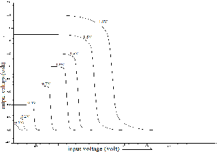
Fig. 2 Inverter VTC showing operation down to 100 mV in a 0.18 µm process.
This section describes the design of various digital CMOS cells in subthreshold. First, the basic CMOS In- verter, shown in Fig. 3, is analyzed in detail and then, based on this analysis, the NAND and the NOR gates are designed and after that other circuits can also be designed by calculating the values of W/L with the help of these
W/L values of Inverter which has been designed for
symmetric output and equal charging and discharging current.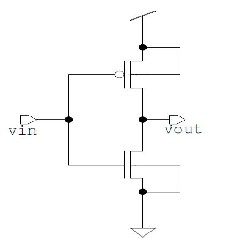
Fig. 3 Basic CMOS Inverter
By simulating this CMOS Inverter using TSMC 0.18 µm
technology, the Inverter’s values of W/L for PMOS = (1.2
µm/0.18 µm) and W/L for NMOS = (0.27 µm/0.18 µm) were obtained for strong inversion operation. While the In-
verter’s values of W/L for PMOS = (3.0 µm /0.18 µm) and
W/L for NMOS = (0.27 µm/0.18 µm) were obtained for sub- threshold operation.
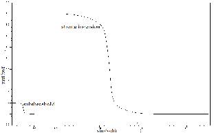
Fig. 4 VTC curves for Inverters operating in strong inversion and subthreshold.
By using these values of W/L of basic Inverter, other circuits can be designed having the equivalent W/L values equal to that of this basic Inverter.
The load capacitance, for the inverter described in pre- vious section, for strong inversion region is 5 fF while the load capacitance for subthreshold conduction is 11 fF.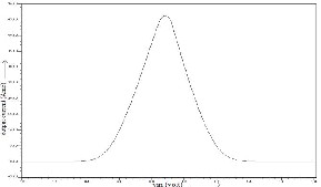
Fig. 5 Output current variation with input voltage in strong inversion
region with Vdd = 1.8 V.
From Fig. 5 and 6, it is clear that the current depends
on input (gate) voltage linearly in strong inversion region and exponentially in subthreshold region.
IJSER © 2010 http://www.ijser.org
International Journal of Scientific & Engineering Research, Volume 2, Issue 2, February-2011 4
ISSN 2229-5518
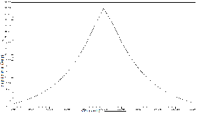
Fig. 6 Output current variation with input voltage in subthreshold
region with Vdd = 0.2 V.
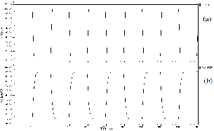
Fig. 7 Simulation result of transient analysis for CMOS Inverter in subthreshold region: (a) Input Signal, (b) Voltage waveform of Out- put Signal.
Two-input CMOS NAND Gate can be designed having the equivalent W/L value equal to that of the Inverter.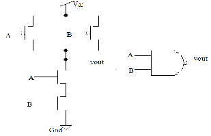
Fig. 8 Basic Structure of a 2-input CMOS NAND Gate
The load capacitance, for the NAND Gate designed, for strong inversion is 10 fF while for subthreshold conduc- tion is 18 fF.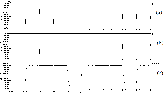
Fig. 9 Simulation result of transient analysis for a 2-input CMOS NAND Gate in subthreshold conduction region: (a) Input Signal (A), (b) Input Signal (B), (c) Voltage waveform of Output Signal (VOUT).
The basic structure and its simulation result of a 2-to-1
CMOS Multiplexer are shown in Fig. 10 and 11.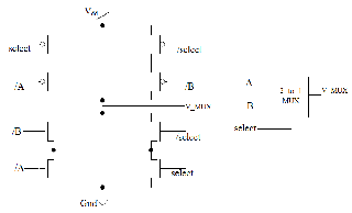
Fig. 10 Basic Structure of a 2-to-1 CMOS Multiplexer
The load capacitance, for the 2-to-1 CMOS Multiplexer designed, for strong inversion is 13 fF while for sub- threshold conduction is 30 fF.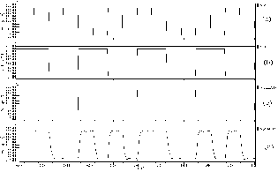
Fig. 11 Simulation result of transient analysis for a 2-to-1 CMOS Multiplexer in subthreshold conduction region: (a) Input Signal (A), (b) Input Signal (B), (c) Input Signal (SELECT) (d) Voltage waveform of Output Signal (V_MUX).
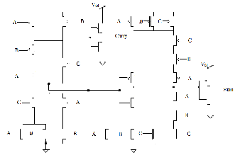
Full Adder is basic structure for any arithmetic circuit, so the design of a Full Adder is also necessary. The basic
IJSER © 2010 http://www.ijser.org
International Journal of Scientific & Engineering Research, Volume 2, Issue 2, February-2011 5
ISSN 2229-5518
structure and simulation result for a One-Bit CMOS Full
Adder are shown in figures given below.
0.030
0.028
V = 0.2 V
dd
L,SUM
= 8 fF
0.026
0.024
0.022
0.020
0.018
0.016
0.014
0.012
C = 8 fF
L,CARRY
1 2 3 4 5
Frequency (KHz)
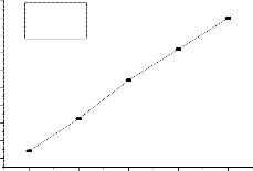
Fig. 14 Power dissipation results for a 1-bit Full Adder operating in subthreshold conduction region.
Fig. 12 Basic Structure of a One-Bit CMOS Full Adder
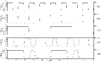
Fig. 13 Simulation result of transient analysis for a One-Bit CMOS Full Adder in subthreshold conduction region: (a) Input Signal (A), (b) Input Signal (B), (c) Input Signal (C), (d) Voltage waveform of Output (SUM) Signal, (e) Voltage waveform of Output (CARRY) Signal.
TABLE I
POWER DISSIPATION IN DIFFERENT CMOS CIRCUITS
Power (nW) | |||
f = 4 kHz | f = 5 kHz | ||
CMOS Inverter | Superthreshold | 389.54 n | 486.93 n |
CMOS Inverter | Subthreshold | 0.002107 n | 0.002576 n |
2-input NAND | Superthreshold | 366.56 n | 442.54 n |
2-input NAND | Subthreshold | 0.002732 n | 0.003382 n |
2:1 MUX | Superthreshold | 869.55 n | 1038.58 n |
2:1 MUX | Subthreshold | 0.004995 n | 0.005414 n |
Full Adder | Superthreshold | 971.15 n | 1100.94 n |
Full Adder | Subthreshold | 0.024413 n | 0.027932 n |
Fig. 14 shows the dynamic power variation with differ- ent clock frequencies for a 1-bit Full Adder operating in subthreshold conduction region.
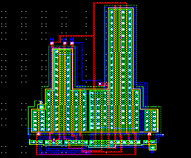
For a 1-bit Full Adder operating in subthreshold con- duction resgion, layout and post-layout simulation results are shown in Fig. 15 and 16 respectively.
Fig. 15 Layout of 1-bit CMOS Full Adder operating in subthreshold conduction region.
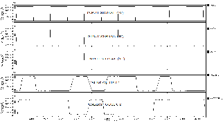
Fig. 16 Post-Layout Simulation – Transient analysis for 1-bit CMOS Full Adder operating in subthreshold conuction region.
IJSER © 2010 http://www.ijser.org
International Journal of Scientific & Engineering Research, Volume 2, Issue 2, February-2011 6
ISSN 2229-5518
Based on the subthreshold conduction, the designing of various digital circuits have been done. The supply volt- age used for the circuits operating in subthreshold con- duction region is 0.2 V. The power analysis also has been carried out for the circuits, operating in subthreshold conduction region and in superthreshold conduction re- gion. It is found that the circuits operating in subthresh- old conduction region provide the significant power re- duction than the superthreshold conduction region.
It can be found that subthreshold conduction region is advantageous in applications where power is the main concern and performance can be sacrificed to achieve the low-power because the speed of a circuit operating in subthreshold conduction region becomes significantly slow.
[1] S. Hanson, B. Zhai, K. Bernstein, D. Blaauw, A. Bryant, L.
Chang, K. K. Das, W. Haensch, E. J. Nowak and D. Sylvester, “Ultralow-voltage, minimum-energy CMOS,” IBM Journal of Research and Development, vol. 50, no. 4-5, pp. 469–490, 2006.
[2] A. P. Chandrakasan, S. Sheng and R. W. Brodersen, “Low Power CMOS Digital Design,” IEEE Journal of Solid-state Cir- cuits, vol. 27, no. 4, pp. 473-484, April 1999.
[3] K. Ragini and B. K. Madhavi, “Ultra Low Power Digital Logic Circuits in Subthreshold for Biomedical Applications,” Journal of Theoretical and Applied Information Technology, 2005.
[4] K. Roy, S. Mukhopadhyay, and H. Mahmoodi-Meimand, “Leakage current mechanisms and leakage reduction tech- niques in deep-submicrometer cmos circuits,” in Proceedings of IEEE, vol. 91, no. 2, pp. 305-327, 2003.
[5] R. Corless, G. Gonnet, D. Hare, D. Jeffrey and D. Knuth, “On the Lambert W function,” Advance in Computational Mathemat- ics, vol. 5, pp. 329-359, 1996.
[6] A. Wang, B. H. Calhoun and A. P. Chandrakasan, Subthreshold
Design For Ultra Low-Power Systems, Springer, USA, 2006.
[7] R. M. Swanson and J. D. Meindl, "Ion-Implanted Complemen- tary MOS Transistors in Low-Voltage Circuits," IEEE Journal of Solid-State Circuits, vol. 7, no. 2, pp. 146-153, April. 1972.
[8] S. M. Kang and Y Leblebici, CMOS Digital Integrated Circuits:
Analysis and Design, 3rd ed, McGraw Hill, 2004.
IJSER © 2010 http://www.ijser.org