International Journal of Scientific & Engineering Research Volume 2, Issue 3, March-2011 1
ISSN 2229-5518
Design of HDLC Controller Using VHDL
K.Sakthidasan, Mohammed Mahommed
Abstract- In this paper, we explore a High-level Data link control published by International Standards Organization (ISO). HDLC is one of the most enduring and fundamental standards in Communications. HDLC is in itself a group of several protocols or rules for transmitting data between network points. The HDLC protocol also manages the flow or pace at which the data is sent. The data is organized into a unit called a frame. HDLC controllers are devices, which executes the HDLC protocol. Some of the key operations of the HDLC protocol implemented are handling bit oriented protocol structure and formatting data as per the packet switching protocol, it includes Transmitting and receiving the packet data serially and providing the data transparency through zero insertion and deletion. This controller generates and detects flags that indicate the HDLC status. The device contains a full duplex transceiver, with independent receive and transmit sections for bit-level HDLC protocol operations. The design is completely Synchronous, with separate clock inputs for receive and transmit allowing the two sections to operate asynchronously. These operations have been implemented using VHDL.
Index Terms- HDLC, VHDL, Bit-level HDLC protocol operations.
1. INTRODUCTION
1.1 Overview of HDLC:
The high level data link control (HDLC) protocol Defined by the ISO provides a transparent transmission Service at the data link layer of the ISO reference model. Many protocol suites use an HDLC link layer, including X.25, The IP point-to-point protocol (PPT) and SNA. It has been so widely implemented because it supports half duplex and full duplex communication lines, point-to-point (peer to peer) and multipoint networks, and switched or non switched channels. The procedures outlined in HDLC are designed to permit synchronous, code-transparent data transmission. The HDLC Protocol is a general purpose protocol, which Operates AT the data link layer of the OSI reference model. The protocol uses the services of a physical layer, to provide communications path between the transmitter and receiver. The users of the HDLC service provide PDUs, which are encapsulated to form data link layer frames. These frames are separated by HDLC “flags” and are modified by “Zero bit insertion” to guarantee transparency. Each piece of data is encapsulated in an HDLC frame by adding a trailer and a header. The header contains an HDLC address and an HDLC control field. The trailer is found at the end of the frame, and contains a Cyclic Redundancy Check (CRC), which detects any errors, which may occur during transmission. The frames are separated by HDLC flag sequences that are transmitted between each frame and whenever there is no data to be transmitted.
1.1.1 HDLC Frame Structure
HDLC uses the term "frame" to indicate an entity of data (or a protocol data unit) transmitted from one station to another. Figure below is a graphical representation of a HDLC frame with an information field.
Fig 1- HDLC Frame Structure
Field Name Size(in bits) Flag Field (F) 8 bits Address Field (A) 8 bits Control Field (C) 8 or 16 bits
Variable; Not used in some
Information Field (I)
frames
Frame Check Sequence (FCS) 16 or 32 bits
Closing Flag Field (F) 8 bits
The Flag Field
Every frame on the link must begin and end with a flag sequence field (F). Stations attached to the data link must continually listen for a flag sequence. The
flag sequence is 01111110. Flags are continuously
IJSER © 2011 http://www.ijser.org
International Journal of Scientific & Engineering Research Volume 2, Issue 3, March-2011 2
ISSN 2229-5518
transmitted on the link between frames to keep the link
active. Two other bit sequences are used in HDLC as ` signals for the stations on the link. These two bit sequences are:
• Seven 1's, but less than 15 signals an abort signal.
The stations on the link know there is a problem
on the link. 0 1
• 15 or more 1's indicate that the channel is in an idle state.
0 1
HDLC is a code-transparent protocol. It does not rely on a specific code for interpretation of line control. This means that if a bit at position N in an octet has a specific meaning, regardless of the other bits in the same octet. If an octet has a bit sequence of 01111110, but is not a flag field, HLDC uses a technique called bit-stuffing to differentiate this bit sequence from a flag field.
Once the transmitter detects that it is sending 5 consecutive 1's, in inserts a 0 bit to prevent a flag sequence occurring. At the receiving end, the receiving station inspects the incoming frame. If it detects 5 consecutive 1's it looks at the next bit. If it is a 0, it pulls it out. If it is a 1, it looks at the 8th bit. If the 8th bit is a 0, it knows an abort or idle signal has been sent. It then proceeds to inspect the following bits to determine appropriate action. This is the manner in which HDLC achieves code-transparency. HDLC is not concerned with any specific bit code inside the data stream. It is only concerned with keeping flags unique.
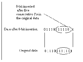

Fig 2 -Bit Insertion

Start
Fig 3 -Flowchart for Bit Deletion
The Address Field:
The address field (A) identifies the primary or secondary stations involvement in the frame transmission or reception. Each station on the link has a unique address. In an unbalanced configuration, the A field in both commands and responses refer to the secondary station. In a balanced configuration, the command frame contains the destination station address and the response frame has the sending station's address.
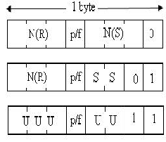
The Control Field:
HDLC uses the control field(C) to determine how to control the communications process. This field contains the commands; responses and sequences numbers used to maintain the data flow accountability of the link, define the functions of the frame and initiate the logic to control the movement of traffic between sending and receiving stations. There three control field formats:
Count five 1s and one 0
IJSER © 2011 http://www.ijser.org
International Journal of Scientific & Engineering Research Volume 2, Issue 3, March-2011 3
ISSN 2229-5518
Fig 4 -Control Field Format
Information Transfer Format
The frame is used to transmit end-user data between two devices.
Supervisory Format
The control field performs control functions such as acknowledgment of frames, requests for re- transmission, and requests for temporary suspension of frames being transmitted. Its use depends on the operational mode being used.
Unnumbered Format
This control field format is also used for control purposes. It is used to perform link initialization, link disconnection and other link control functions. The 5th bit position in the control field is called the poll/final bit, or p/f bit. It can only be recognized when it is set to 1. If it is set to 0, it is ignored. The poll/final bit is used to provide dialogue between the primary station and secondary station. The primary station uses P=1 to acquire a status response from the secondary station. The P bit signifies a poll. The secondary station responds to the P bit by transmitting a data or status frame to the primary station with the P/F bit set to F=1. The F bit can also be used to signal the end of a transmission from the secondary station under Normal Response Mode.
The Information Field
This field is not always in a HDLC frame. It is only present when the Information Transfer Format is being used in the control field. The information field contains the actually data the sender is transmitting to the receiver.
The Frame Check Sequence Field
This field contains a 16 bit, or 32 bit cyclic redundancy check. It is used for error detection. CRC-16 = x16 + x15 + x2+ 1 is used.
2. Overview of VHDL:
VHDL is the VHSIC Hardware Description Language. VHSIC is an abbreviation for Very High Speed Integrated Circuit. It can describe the behavior and structure of electronic systems, but is particularly suited as a language to describe the structure and behavior of digital electronic hardware designs, such as ASICs and FPGAs as well as conventional digital circuits. VHDL is a notation, and is precisely and completely defined by the Language Reference Manual (LRM). This sets VHDL apart from other hardware description languages, which are to some extent defined in an adhoc way by the behavior of tools that use them. VHDL is an international standard, regulated by the IEEE. The definition of the language is non-proprietary. VHDL is not an information model, a database schema, a simulator, a toolset or a methodology! However, a methodology and a toolset are essential for the effective use of VHDL. Simulation and synthesis are the two main kinds of tools, which operate on the VHDL language. The Language Reference Manual does not define a simulator, but unambiguously defines what each simulator must do with each part of the language. VHDL does not constrain the user to one style of description. VHDL allows designs to be described using any methodology — top down, bottom up or middle out! VHDL can be used to describe hardware at the gate level or in a more abstract way. Successful high- level design requires a language, a tool set and a suitable methodology. VHDL is the language; you choose the tools, and the methodology.
2.1 Simulation
Top-down design first describes a system at a very high level of abstraction, like a specification. Designers simulate and debug the system at this very high level before refining it into smaller components. The method describes each component at a high level and debugs it alone and with the other components in the system. The design continues to be refined and debugged until it is complete down to its lowest building block. Mixed-level design occurs when some components are at a more detailed level of description than others. The advantage of the top-down design methodology is that engineers can discover and correct system problems early in the design cycle. Engineers can concentrate on overall design issues such as system requirements and timing. The tedious task of gate-level design can be left to synthesis tool. The bottom line is reduced cost and faster time to manufacturing.
IJSER © 2011 http://www.ijser.org
International Journal of Scientific & Engineering Research Volume 2, Issue 3, March-2011 4
ISSN 2229-5518
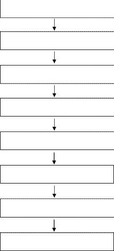
2.2 VHDL design flow: Specification Algorithm
Coding Simulation Synthesis
Place and Route
FPGA ASIC
Fig 5- Design Flow
2.3 Need for a HDLC controller
As mentioned already, HDLC protocol is used widely in many applications. In many situations, the space occupied is a main criterion. Further, compatibility and processing speed pose a serious problem. In order to overcome these difficulties, the solution has been to bring out the protocol converter in the form of a handy controller. The controller can be implemented in two ways. As an embedded application or as a VLSI chip. The data transferred in the overall communication chip is purely digital and also at a very high data rate. Hence the more apt solution is to use the VLSI chip to construct the HDLC controller.
Further, in many applications the processing would need a central controller to monitor the entire process but the space constraint would dictate the need for minimal space occupation. In such a situation, the use of a system there becomes impossible. There arises the need for a controller. Replacement of the system is achieved through such efficient processors.
Transmitter :
The transmitter portion of the HDLC core will begin to transmit when the user’s external logic asserts the TX_DATA_VALID signal. The transmitter will respond by asserting the TX_LOAD signal to load the first byte of the packet. The timing diagram assumes that IDLE_SEL is tied to a ‘1’ and the transmitter is generating continuous ‘1’ bits between frames. If IDLE_SEL is set to a ‘0’, the number of clocks from the assertion of TX_DATA_VALID to TX_LOAD will vary from 5 to 12. Before the transmitter can begin to send data serially, it must send an opening flag (7E). Immediately after the flag is sent, the first byte is clocked out of the input shift register. Once a transmit frame has begun, the user is required to make sure that data is available for each subsequent requested byte. The transmitter will continue to request data by asserting TX_LOAD until the user supplies a TX_EOF signal. This informs the transmitter that the last byte is on the data bus. The transmitter then appends a 16- or 32-bit Frame Checking Sequence (FCS) to the transmitted data. After the FCS is sent, a closing flag (7E) byte is appended to mark the end of the frame.
Receiver :
The receiver clocks serial HDLC frames in continuously through the RXD pin. When an opening flag is recognized, the receiver locks to all subsequent octet bytes. The user informs the receiver of the ability to store the frame by asserting the RX_SPACE_AVAILABLE input. The receiver informs the user that a data byte is available by asserting the RX_READY signal. The receiver indicates the beginning of the frame by asserting the RX_SOF signal. Bytes will continue being passed to the user until the receiver recognizes the closing flag. At this point, the last byte of the FCS sequence will be passed to the user coincident with the RX_EOF signal. It must be stressed that the core does not contain the additional pipeline registers to "swallow" the 2 or 4 bytes of FCS, and these will therefore be passed on to the user.
If this is undesirable, the corresponding pipeline should
IJSER © 2011 http://www.ijser.org
International Journal of Scientific & Engineering Research Volume 2, Issue 3, March-2011 5
ISSN 2229-5518
be added externally to keep these bytes from passing on as part of the received frame. After the reception of the
frame has completed, the receiver will pass a byte of
status information to the user by placing the status on the receive data bus and asserting the RX_STATUS signal.
| 8 bit parallel | | 16/32 bit | | Zero | | Flag & | |
TX_DATA | to serial shift register | | FCS generator | | Insertion | | abort Generation | TXD |
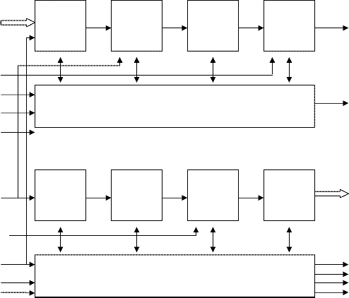
IDEL_SEL
TX_Data_valid TX_LOAD
TX EOF
TXC
TRANSMIT CONTROL
| Flag & | | Zero | | 16/32 bit | | 8 bit | |
RXD | abort deletion | | detection | | FCS checker | | parallel to serial shift | RX_DATA [7:0] |
| | | | | | | register | |
FCS 16/32
RX_READY RX_Space_Avail RX_SOF
RXC
RECEIVER CONTROL
RX_EOF
RESET RX_STATUS
Fig 6- HDLC Controller Block Diagram
memory hierarchy to manage fast access to RAM on and off the chip . A comparison between the implemented HDLC
3. TESTING PROCESS USING VHDL:
The HDLC transceiver was designed and implemented using VHDL codes. The codes were simulated by ModelSim by forcing the clock and values to other input pins and monitoring the output waveforms. The reason for using Virtex FPGA is its various built-in features that help the designer throughout the process of design.This family provides a broad capability for chip-to-chip communications through programmable support forthe latest I/O standards, digital Delay-Locked Loops (DLLs) for clock signal synchronization on the FPGA and on the board, and a
transceiver in this research and some of the major existing products is presented in Table 3.The waveforms have been included below.
IJSER © 2011 http://www.ijser.org
International Journal of Scientific & Engineering Research Volume 2, Issue 3, March-2011 6
ISSN 2229-5518
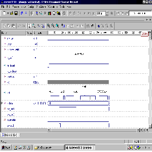
Fig 7- Waveform for Transmitter simulated output
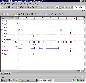
Fig 8-Waveform for Receiver simulated output:
4. CONCLUSION
HDLC Controllers are deployed within a number of different data networking applications. Being built on the capabilities of the Virtex family and due to its features and cost effectiveness. Hence it is uniquely poised to penetrate the ASSP marketplace. An FPGA based HDLC controller solution with efficient partitioning of hardware and software functions provides the necessary scalability and flexibility to handle all these applications and allows for tracking of new standards.
Thus through this project it is clear that to reduce the cost
of design and to increase the probability of the IC design, FPGA design helps the designer in many ways. Thus it reduces the time consumption in designing as well as in testing the design. The coding written in VHDL language was checked using ALTERA simulator. The top level coding written for this paper is tested along with random stimulator values and the results obtained were up to the designer’s expectation. The future enhancement in this paper is to implement this controller in real time application and also to accommodate more number of channels in the same design. Thus this controller can be used to provide communication by accommodating more number of channels using PCM highway technique.
5. FUTURE ENHANCEMENTS:
This paper can be used as Multi-channel HDLC controller with few modifications in the VHDL coding. The main difference single channel and multi channel HDLC controller is that a multiplexer and a demultiplexer are used in the transmitter and receiver respectively. The main advantage of this project is error correction using CRC-16 polynomial and through this controller we can achieve error free communication. Thus this project can be used in MODEMS where error detection part is performed by this HDLC controller.
Since, HDLC forms the basic standard for other protocols
like LAPB, LAP, LLC, LAN etc., this controller can be used to generate frame for any of these protocols with slight modification in the coding part. This HDLC controller can also support ISDN frame format and thus the flexibility in this controller is very high.
REFERENCES:
[1] Guozheng Li Nanlin Tan State Key Lab. of Rail Traffic Control & Safety, Beijing Jiaotong Univ., Beijing, China “Design and Implementation of HDLC Protocol and Manchester Encoding Based on FPGA in Train Communication Network”,
IJSER © 2011 http://www.ijser.org
International Journal of Scientific & Engineering Research Volume 2, Issue 3, March-2011 7
ISSN 2229-5518
Information and Computing (ICIC), 2010 Third
International Conference
[2] Lu, Y., Z. Wang, L. Qiao and B. Huanq, 2002. "Design and implementation of multi-channel high speed HDLC data processor," IEEE International Conference on Communications, Circuits and Systems, and West
Sino Expositions, 2: 1471-1475
[3] Amendola, A.M. Benso, A. Corno, F.
Impagliazzo, L. Marmo, P. Prinetto, P.
Rebaudengo, M. Sonza Reorda, M. CRIS, Napoli “Fault behavior observation of a microprocessor system through a VHDL simulation-based fault injection experiment Design Automation Conference, 1996, with EURO-VHDL '96 and Exhibition, Proceedings EURO-DAC '96, European ,16-20 Sep 1996
[4] Arshak, K. Jafer, E. McDonagh, D. Ibala, C.S.
Univ. of Limerick, Limerick, “Modelling and simulation of wireless sensor system for health monitoring using HDL and Simulink mixed environment” Computers & Digital Techniques, IET Sept. 2007
[5] Gheorghiu, V., S. Kameda, T. Takagi, K.
Tsubouchi and F. Adachi, 2008. "Implementation of frequency domain equalizer for single carrier transmission," In Proceedings of the 4th
International Conference on Wireless Communications, Networking and Mobile Computing, WiCOM '08.
[6] Jun Wang; Wenhao Zhang; Yuxi Zhang; Wei Wu; Weiguang Chang; Sch. of Electron. & Inf. Eng., Beihang Univ. (BUAA), Beijing, China “Design and implementation of HDLC procedures based on FPGA” , Anti- ounterfeiting, Security, and Identification in Communication, 2009. ASID
2009. 3rd International Conference, 20-22 Aug.
2009
[7] Meng, X. and V. Chaudary, 2009. "Boosting data throughput for sequence database similarity searches on FPGAs using an adaptive buffering scheme," Parallel Computing, 35(1): 1-11.“
IJSER © 2011 http://www.ijser.org