Sarhad University of Science and Information Technology,
Peshawar, Pakistan. engrfaheem@yahoo.com1, habbas33@gmail.com2 haider_101@hotmail.com3, alibintahir@gmail.com4
International Journal of Scientific & Engineering Research, Volume 4, Issue 8, August-2013 19
ISSN 2229-5518
Electrical Engineering Department,
Sarhad University of Science and Information Technology,![]()
Peshawar, Pakistan. engrfaheem@yahoo.com1, habbas33@gmail.com2 haider_101@hotmail.com3, alibintahir@gmail.com4
Abstract — Microwave power amplifiers are the most significant components in wireless communications systems. As the technology continue to progress, the designers are facing new challenges and opportunities. The purpose of this work is to push the limits of efficiency and bandwidth of power amplifiers. The objective of this research is to design and build a prototype two stage Microwave power amplifier operated at 2.4 GHz with a linear region of operation up to our desired output of 0.5 watt or 27 dBm. The transistor used in the first stage is BFP540 while the output power of the first stage is the input of the second stage in which the ATF50189 transistor is used to for amplification. All the simulations and readings are taken by using AWR Microwave Office software. By using the load line Rl and the biasing points are achieved for both stages. The applications of our proposed device include many products in the field of microwave communications. One of the important applications of a Microwave power amplifier is in the output stage of a transmitter where a signal needs amplification before it is transmitted.
Keywords — Class A Microwave Power Amplifier, Two Stage Amplifier, AWR Microwave Office
—————————— ——————————
RF power amplifiers function very differently from small- signal amplifiers. Power amplifiers operate with large signals, and the active devices display strong nonlinear behavior. The amplifier output may be modeled as an infinite power series consisting of nonlinear terms added to a linear term and a dc offset. The power series coefficients depend on the transistor operating point (dc bias point, or the average operating point) and are considered constant to changes in the input and output RF signal. However, all models have a serious limitation in that they can only accurately model weak nonlinear circuits for which the power series coefficients are almost constant (a narrow operation zone around the de-bias point). In a large-signal power amplifier, nonlinear effects are very strong because transistor parameters depend on many factors, including the input and output matching network Configuration and the input and output signal amplitudes and waveforms. In addition, the active device may be driven into saturation or cut-off for a certain portion of the RF cycle. Modeling these strong nonlinear effects is a very difficult task [5].
The Class A amplifier presents a linear transfer characteristic and a high power gain (20 to 30 dB, even at high frequencies). However, because of their low efficiency level, Class A amplifiers are most often used as low-level drivers for more efficient PAs. In such applications, the Class A amplifier consumes only a small portion of the total DC power, and the overall efficiency of the amplifying chain is not significantly affected. Class A RF PAs are also used for laboratory equipment (for example, very low- distortion linear wideband amplifiers) or at microwave frequencies where it could be difficult to employ other classes of amplification[4]. The basic circuit and the
operation of the Class A RF PAs are quite similar to those of the small-signal Class A amplifier. There is no dividing line between small-signal and Class A PAs.
In this research we have designed two stage microwave power amplifier having the operation frequency 2.4 GHz ISM (Industrial, Scientific, and Medical) Band in AWR Microwave office to achieve the gain of +10~12dB and output power of 0.5 Watt (27dBm) within the size of 2.5x2.5 inch.
To design a microwave power amplifier the first thing we need is the static IV curves of a proper transistor which can provide the desired frequency, output power and gain etc. Secondly, we designed the input and output circuits using smith chart for adequate matching. Finally, the stability issues are addressed. It is very obvious that a working circuit may not be stabilized at some point which is not bearable. Stability circles are used to check whether the circuit is stabilize or not if the circuit is not stabilize various techniques are used to stabilize it according to the condition.
To design the complete circuitry the transistor’s selected are BFP540 for the first stage and ATF50189 for the second step because these transistors were matched with the specifications.
The first stage in which BFP540 was used the model was easily achieved from the Infenion official web site in .awr format which is shown in Figure 1.
IJSER © 2013 http://www.ijser.org
International Journal of Scientific & Engineering Research, Volume 4, Issue 8, August-2013 20
ISSN 2229-5518
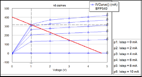
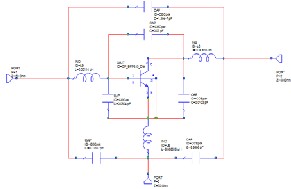
Figure 1: Non Linear circuit of BFP540 (.awr)
ATF50189 is a packaged Aluminum Gallium Arsenide / Indium Gallium Arsenide (AlGaAs/InGaAs) pseudomorphic High Electron Mobility Transistor (pHEMT). This transistor was chosen because it met all of the requirements for the targeted specifications. The most tedious part of the starting stage was to find the nonlinear (.awr) file of the transistors. for the second stage it became a night mare as the .awr file was not on any link so it was decided to use the ADS model .We first open the model in ADS software and took a screen shot from it then the same model was designed in AWR microwave office both the screen shot and the AWR designed model can be seen in Figure 2.
Figure 3: V-I Curves for BFP540 (.awr)
Using a load line we achieve 4.7 volts and 0.4 amp through which we found the Rl. while from the mid of this load line the Vce and I be is achieved i.e.
Rl = 4.7𝑣 0.4𝐴 =11.75ohm
Vce = 2.7v
Ibe = 170mA
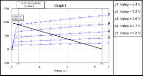
Figure 4: V-I Curves for ATF50189 (.awr)
Here, we achieve 6.5 volts and 0.98 amp through which we found the Rl. And the from the mid of this load line the Vds and Vgs is achieved. i.e.
Rl = 6.5𝑣 0.980𝐴 =6.633ohm
Vds = 3.00v
Vgs = 0.54v
1: Circuit Diagram for ATF50189(.awr)
Figure
To design a matching circuit smith chart is used for which
The achieved RL is then translated on the smith chart for 50
Ohm impedance line. On the smith chart the translated
point is then mapped and starting from the mid of the
smith chart i.e. one and ending on the RL point, a circuit is achieved which shows as the corresponding lumped elements. These lumped elements then made the output
In order to obtain maximum power from this device, we
must define a load line that fully spans these usable regions. The slope of this load line will determine the large-signal load impedance, RL, for maximum transistor output power. In other words, RL is used as the goal impedance to be presented to the device’s drain terminal by the output circuit in order to achieve maximum RF power output.
To obtain VI curves we configure the circuit providing with the VSWEEP from 0V to 5V with the step size of 1V for BFP540. Whereas, VSWEEP from 0V to 7V with the step size of 0.1V for ATF50189. These VI- Curves can be seen below in figure 3 and 4.
portion of the circuit. By achieving the output portion it is
then easy to draw the input circuit. Because the circuit was
to be built on a substrate, a mixed lumped element microstrip design had to be generated based on the above design. This is because every connection between all of the elements are in actuality microstrip pieces and therefore had to be considered and modelled in the design. This was a very long and drawn out process but it finally yielded a working circuit. This is the final circuit in Microwave Office along with the S-parameters and 27 dB compression point determination. These S-parameters are shown below in figure 5 and figure 6.
IJSER © 2013 http://www.ijser.org
International Journal of Scientific & Engineering Research, Volume 4, Issue 8, August-2013 21
ISSN 2229-5518
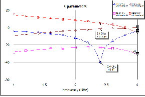
Figure 5: S-parameters of first stage using BFP540
From the Figure it is clear that the circuit is well matched at
2.4 GHz and S12 is also very low which is good as it shows
the reflected gain at input side, S21 shows the gain at output which is 5.017dB.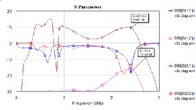
Figure 6: S-parameters of second stage using ATF50189
Above figure shows that stage 2 is the well matched circuit at 2.4 GHz having low S12 and S21 shows the gain at output which is 9.845dB.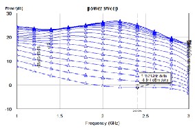
The total power which is achieved using software is shown in the Figure 7 for BFP540 and ATF50189 in Figure 8. In these Figures the input power is varied due to which the output power varies from one point to the other. Therefore, the values which are required to gain a specific output power should be selected.
Figure 7: Total Power Sweep (BFP540)
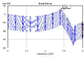
Figure 8: Total Power Sweep (AFT50189)
In the above figures we performed the input power sweep from -5dBm to 30dBm and obtained the output power from
-8.44dBm to 25dBm for BFP540. Whereas, the output power varies from -41dBm to 8.9dBm for the different frequencies as shown above. In addition, we can see a dip in the output power in the second stage after 2.4GHz due to the transistor’s rating.
In this research, a microwave two stage Power Amplifier using AWR Microwave Office was designed .The requirements were that it should have BFP540 transistor in the first and ATF50189transistor in the second stage ,the output power should be 27db and the size of the amplifier should be less than two and half inches it is concluded that as the circuit is behaving linearly as can be seen and observed from the test results so further to design the amplifier the circuit scan be designed using an S2p files which are for linear devices .by using these files an amplifier for 2.4 GHz can be designed easily which will give a lot of gain for the desired frequency.
[1] Grebennikov and N. Sokal, Switchmode RF Power Amplifiers.
Newnes, 2007.
[2] G. Gonzalez, Microwave Transistor Amplifiers Analysis and
Design. Prentice Hall, 1997.
[3] M. Iwamoto, A. Williams, P.-F. Chen, A. etzger, L. Larson, and P.
As-beck, “An extended doherty amplifier with high efficiency over a wide power range," Microwave Theory and Techniques, IEEE Transactions on, vol. 49,no. 12, pp. 2472 -2479, dec 2001.
[4] Rosen, M. Stuchly, and A. Vander Vorst, “Applications of
rf/microwaves in medicine," Microwave Theory and Techniques, IEEE Transactions on, vol. 50, no. 3, pp. 963-974, Mar 2002.
[5] H. Sobol and K. Tomiyasu, “Milestones of icrowaves," Microwave
Theory and Techniques, IEEE Transactions on, vol. 50, no. 3, pp.
594-611, Mar 2002.
[6] S. C. Cripps, RF power amplifiers for Wireless communications.
Artech House, 2006.
[7] D.-T. Wu, D. Frebrowski, and S. Boumaiza, “First-pass design of high efficiency power amplifiers using accurate large Signal models," in Wireless and Microwave Technology Conference
(WAMICON), IEEE 11th Annual,12-13 2010, pp. 1-4.
IJSER © 2013 http://www.ijser.org