International Journal of Scientific & Engineering RESEARCH, VOLUME 3, Issue 6, June-2012 1
ISSN 2229-5518
Avigyan Datta Gupta,Chirashree Roy Chaudhuri
Abstract –In this paper a design and analysis of an array of 100nm thin film MEMS based microheater on SOI wafer is presented. The microheater is constructed on a SOI wafer where temperature rise of 2000C is achieved with minimum power consumption of 20mW .Also there is minimum heat loss through the substrate. The temperature rise is concentrated in only the microheater region and there is excellent uniformity in the temperature distribution in both the microheaters.Stress and displacement analysis is also carried out for the structure and the result is satisfactory.
Index Terms—MEMS,microheater,FEM, micromachining,SOI wafer, heat loss, temperature, stress, minimum power loss.
—————————— ——————————
insulator) substrates are being deployed [7],[8][9].We have
Semiconducting metal oxides like SnO2, ZnO, TiO2 have
long been used for detecting poisonous (CO) and inflammable gases(CH4) by their change in conductivity. Previously gas sensors used to have relatively high power consumptions (of the order of 500mW -2W) due to their excessive thermal mass[1],[2][3].More over response time was also very high. The bottom line in the design and manufacture of modern gas sensors is the transfer from ceramic (of Figaro type) to thin film gas sensors. This transfer provides new opportunities for further miniaturisation, low power consumption and cost reduction of gas sensors. Microheaters for them have been designed and optimized. But with MEMS based microheater which is incorporated to maintain a particular
temperature (the temperature at which the sensitivity of the
metal oxide is maximum) ,provides several advantages
such as the proper thermal isolation between sensor element and substrate,low power consumption(30-150 mW)[4],[5],[6],ease of microheater array fabrication and small size. For compactness and cicruit inerrability of the microheater based gas sensor array, SOI (silicon-on –
————————————————
![]() Avigyan Datta Gupta,B.Tech,Electronics & Instrumentation Engineering Department, Future Institute of Engineering & Department(Affiliated to West Bengal University of Technology),e-mail: avigyan1@gmail.com
Avigyan Datta Gupta,B.Tech,Electronics & Instrumentation Engineering Department, Future Institute of Engineering & Department(Affiliated to West Bengal University of Technology),e-mail: avigyan1@gmail.com
![]() Chirashree Roy Chowdhury,Assistant Professor,Electronics &
Chirashree Roy Chowdhury,Assistant Professor,Electronics &
Telecommunications Engineering department,Bengal Engineering & Science University,Shibpur,e-mail: chirosreepram@yahoo.com
Developed here MEMS based array of microheater structure for gas sensor applications whereby the temperature achieved is 2000C and power consumption is only 20mW with uniform temperature distribution over the microheater and minimum heat loss through the substrate. We have used coventorware 2010 (capable of performingFEM analysis) [10],[11] in our design and analysis and all the 3D Figs. that are presented here are tetrahedrally meshed in coventorware 2010.
We have used the following materials in our design and their properties are given in TABLE 1 and TABLE 2.The materials and their properties are given in the material database of coventorware 2010.
TABLE 1
MATERIALS USED AND THEIR PROPERTIES
IJSER © 2012 http://www .ijser.org
International Journal of Scientific & Engineering RESEARCH, VOLUME 3, Issue 6, June-2012 2
ISSN 2229-5518
Therm Oxide | 20.15e-15 | 5.0e-7 | 1.0e-4 |
TABLE 2
MATERIALS USED AN THEIR PROPERTIES
2.3 Whole Structure Design
We have used 4 basic layers in the SOI wafer as shown in Fig.2.On top of therm oxide-1 of Fig.2,microheater is designed.
therm oxide -2 silicon-2
therm oxide-1 Silicon-1
We have used the microheater structure as shown in
Fig.1.The thickness of the microheater is 0.1µm and total length is 420µm.The microheater is made of platinum .The bond pad & bond pad contact have additional 0.1µm of gold coated on them.The dimension of Bond Padd is 500µm X 500µm and the dimension of the bond pad contact is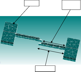
450µmX2µm.
bond bond pad contact
microheater
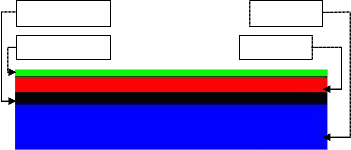
Fig.2 The 4 basic layers od SOI wafer in 2D view.
The therm oxide-1(green colour) and therm oxide-2( black colour) are both of 2µm thick whereas silicon-1(red colour) and silicon-2(blue colour) are of 2µm and 10µm thick respectively.The basic aim is to construct the microheater
on the SOI wafers.After we have grown the 4 basic layers of
SOI wafer as shown in Fig.2 and above it the microheater
as shown in Fig.1,we used the MEMS technology i.e surface
and bulk micromachining technology to have the required structure as shown in Fig. 3(top viw),Fig.4(closer top
view) and Fig.5 (bottom view) which lead us to our analysis and desired results.There is a through hole in the middle of the structure(ie all the 4 layers are etched out from the through hole region).There are 2 membranes and 4 flexures in the through hole region.The 2 membranes are connected to the SOI wafer via flexures as shown in Fig.3 and Fig.4.Both the membranes and flexures are actually the therm oxide-1 layer (of same thickness ie 2µm).We have
also grown 2 free dangling silicon structures(of same dimension as that of the membrane) and is plugged to the bottom of the 2 membranes respectively.The purpose of the dangling structure is to absorb heat from the membranes i.e they act as heat sinkers.However,there is no dangling silicon grown in the bottom of the flexures.
Fig. 1 Microheater structure in 3D view.
IJSER © 2012 http://www .ijser.org
3
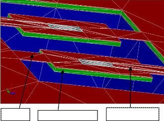
Membrane
flexure free dangling silicon bond pad contact
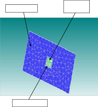
Fig. 4 Closer 3D view of the whole structure focusing the membrane part.
substrate silicon
through hole region
top therm oxide
silicon substrate
free dangling silicon
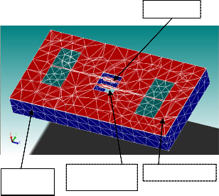
Fig. 3 Top 3D viw of the whole structure.
The whole structure i.e the entire chip is of dimension
4mmX2mm. The dimension of the through hole is
500µmX500µm(1250µm from left and right edge and
750µm from the top and bottom edge of the chip) .The
membrane dimension is 300µmX150µm.The microheater is constructed in the middle of the membrane,which has a dimension of 100µmX50µm(100µm from left and right edge and 36µm from the top and bottom edge of the membrane).The dimension of the flexure is 100µmX50µm. The main objective of such design is to have our desired temperature of about 2000C in the microheater region with minimum power consumption and so that there is minimum heat loss through the substrate.
microheater membrane
through hole region
through hole region
Fig. 5 Bottom viw of the whole structure in 3D view.
IJSER © 2012 http://www .ijser.org
Total length of the microheater is 420µm.The width and
thichness are 4µm and 0.1µm respectively. Total length/area comes out to 1050µm2.Hence resistence is 115Ω (calculated from specific electrical resistence-1*total length/area,whereby the specific electrical resistence of
4
platinum is 9.009e+12 pS/µm).We have applied 1.5V across the microheater bond pads. The resulting power dissipation is 20mW(calculated from voltage applied2/resistence).The current and the current density found out to be
13mA(calculated from voltage applied/resistence) and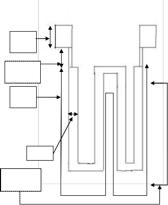
3.2*108pA/µm2(calculatedfrom current/area)respectively.We have used the microheater of the following dimensions as given in Fig.6.
bond pad
bond pad contact
total length
width microheater
region
Fig. 6 2D view of microheater structure.
While designing and simulating the microheater with proper boundary conditions,two main heat considerations which were taken care of are heat loss through conduction and heat loss through convection.
It is the transfer of thermal energy between regions of matter due to a temperature gradient. Heat spontaneously flows from a region of higher temperature to a region of lower temperature, temperature differences over time, approaching thermal equilibrium.It is given by Fourier’s
law of heat conduction
Qx = K1*A*(dT/X), where,
Qx = heat transfer per unit time(W) ,
K1 = thermal conductivity (W/mK) (taken from the material property database of coventorware 2010),
A = Area of material (m2),
dT = temperature difference across the material(K) (taken from the 300k temperature which we have fixed in boundary condition,as discussed in the analysis section),
X = Thickness of the material(m).
Heat energy transferred between a surface and a moving fluid(the fuid here applied is air)at different temperatures is known as convection.It is given by Newton Law of cooling Q = K2 *A*dT,
where,
Q = heat transfer per unit time(W), K2 = convection coefficient (W/mK), A = Area(m2),
dT = temperature difference across the material(K) (taken from the 300k temperature which we have fixed in boundary condition,as discussed in analysis part),
X = Thickness of the material(m).
While designing micoheaters stress analysis should also be performed on the non supportive thin film structures i.e flexures,to analyse wheather such thin film structures can withstand the forces applied on them due to high temperature rise & so that they doesn’t become fragile after fabrication.The stress can be calculated by using the formulae:![]()
E= /Є
Where,
E = Young’s Modulas(Pa)![]()
= Stress(Force applied per unit area)(N/m2 or Pa)
Є = Strain(Change in length,owing to the force apllied,to
the original length)(Dimentionless)
So knowing the Young’s Modulas of a material(from material database of COVENTORWARE 2010),the software calculates the stress developed.
IJSER © 2012 http://www .ijser.org
5
While simulating our MEMS based microheater on SOI
wafer as shown in Fig. 3 we have to apply proper
boundary conditions which will closely resemble the actual scenario post fabrication of the device. So we have covered the whole structure with air 4000µm above and below the structure and 3000µm on the left and right side of the structure as if the whole structure is in an air chamber, as shown in Fig.7.This is very important with respect to heat loss consideration. If we haven’t made this type of structure for analysis then we would have ignored the actual heat loss(of the whole structure) due to convection which will result in an incorrect result.![]()
From the analyzer of coventorware 2010 we have selected the memech option.In the memech domain we have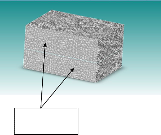
selected the electrothermal analysis(for temperature and current density analysis) and electrothermomechanical analysis(for stress and displacement analysis)..
air chamber(the whole structure is surrounded by air)
Fig. 7 The 3D view of the air chamber structure which surrounds the microheater on SOI wafer structure.
In setting the boundary conditions we have applied we have applied 1.5V across the microheater bond pads and
300K(ie room temperature) is applied everywhere to the
outside surface of the air chamber to take care of heat loss
via conduction and concevtion.Additionally convection
heat loss is taken care of by setting convection coefficient to
5.
We have done 4 analysis which are temperature analysis,current density analysis,stress & displacement analysis and graphical analysis.
From the temperature analysis of Fig.8 we can clearly see that the the microheater is at a temperature of 490K whereas the bond pads are at temperature of 350K,so we can infer that the temperature is mainly concentrated in the microheater region.We can also see that both the microheaters are at the same temperature of 490K.Fig. 9 clearly indicates that there is an excellent temperature distribution throughout the microheater structure from
485K-490K.Fig.10 is the temperature distribution profile of the therm oxide-1 layer which shows that the temperature rise of therm oxide-1 layer is 480K in the microheater region where as in the rest part of therm oxide temperature rise is only 350K. So thermal loss,radiating outwards from region of microheater, is very less.In the flexure part temperature rise is around 420K. The analysis of Fig.11 shows that the temperature rise of the silicon substrate is same everywhere and that temperature is 350K (same as
top therm oxide-1 layer).It also provides the evidence that
heat loss is not only minimum for outward radiating temperature(as in Fig.10) but also for heat radiating downward.
Fig. 8 Temperature profile of the microheater along with bond pad and bond pad contact line.
IJSER © 2012 http://www .ijser.org
6
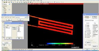
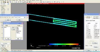
Fig. 9 Temperature profile of the microheater.
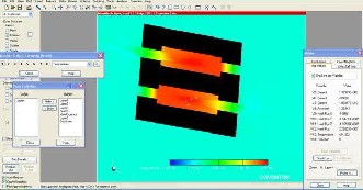
Fig. 10 Temperature profile of the top therm oxide layer.
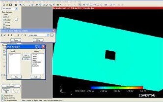
Fig. 11 Temperature profile of silicon substrate.
From Fig. 12, current density is found to be 2.9*108pA/µm2
which nearly matches with our theoritical calculation i.e
3.2*108pA/µm2.
Fig. 12 Current density profile of the microheater.
From Fig. 13,the stress analys yields that stress developed is 327Mpa in the flexure part over which bond pad contact line passes and 27Mpa in the flexure part over which there is no bond pad contact lines. From Fig.14,the displacement of the flexure region is found to be -0.0014571 µm i.e the above stress developed is actually compressive in nature & not tensile From the above analysis we found that the displacement of flexure (owing to stress) is in –ve Z direction i.e the displacement is inside not outside.Also the displacement is very minimam i.e 0.001µm due to thermal effect.As the displacement is –ve we can say that the stress developed is compressive.Now the maximam stress developed in therm oxide-1 layera i.e 326 MPa & 27MPa is within the range of their breaking stress/fracture[12] limit and hence there is no chance of crack or fracture in the post fabrication stage.Since flexure is a thin film layer of therm oxide of 2µm only and there is not supporting layers beneath it and also because of the fact that bond pad contact lines passes over it and microheater region is quite close to it,we have done stress and displacement analysis for it only.
IJSER © 2012 http://www .ijser.org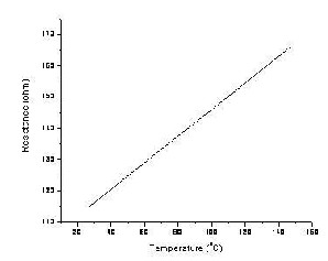
7
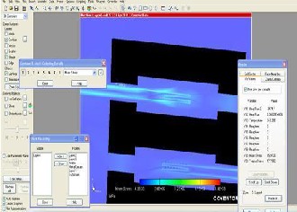
Fig. 13 Stress analysis of the top therm oxide.
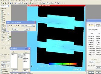
Fig. 14 Displacement analysis of top therm oxide.
From the above analysis of the microheater we have plotted 3 graphs as given in Fig. 15,Fig. 16 and Fig.17 which will give a clear picture of the relationship between resistence vs temperature (i.e gives an idea about the TCR of the platinum microheater),temperature vs voltage(ie for what voltage what temperature is achieved in the microheater) and temperature vs power (ie how temperature rise of the microheater is related to power consumption of the chip at that particular temperature) respectively.
Fig. 15 Resistence Vs temperature graph of microheater.
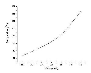
Fig. 16 Temperature Vs voltage graph of microheater.
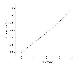
Fig. 17 Temperature Vs power consumption graph of microheater
IJSER © 2012 http://www .ijser.org
8
In this paper we are mainly focused in the design and analysis of MEMS based microheater array on SOI wafer for low power gas sesnsor applications,which is carried out successfully, achieving all the goals which is aimed at mainly the successful design & simulation of array of microheaters on SOI wafer using surface and bulk micromachining(in coventorware 2010) which results in the temperature rise of about 200oC with minimam thermal loss and with minimam power consumption of 20mW only.There is excellent uniformity in the temperature distribution of both the microheaters (the temperature distribution approximately ranges from 2000C-2100C). Simple fabrication steps(using surface and bulk
machining) are being deployed to achieve the structure.The stress analysis is also carried out in order to find out wheather the thin film therm oxide-1 layer in the flexure region can withstand the heat generated and the result is positive.The displacement magnitude clearly indicates that there will be minimam displacement of the flexure on the account of stress.
ACKNOWLEDGMENT
The authors would like to thank Professor S.K.Lahiri of Bengal Engineering and Science University,Shibpur for his erudite guidance in this design and analysis.The authors would also like to thank Professor Hiranmay Saha ,Mr Avra Kundu and Mr Sugato Ghosh of Bengal Engineering and Science University, Shibpur for their valuable advices.
REFERENCES
[1] Isolde Simon, Nicole Barsan, Michael Bauer, U. Weimer,
“Micromachined metal oxide sensors:
opportunities to improve sensor performance”, Sensors and
Actuators, B73, ELSEVIER, 9-12.
[2] P.Hille, H.Strack,”A heated membrane for a capacitive gas sensor”, Sensors and Actuators,A32 (1992)
321-325.
[3] U.Grigull, H.Sandner, Warmeleitung, Springer, Berlin,
1979
[4] S. Astie, A. Gue, E. Schield, L. Lescouzeres. A. Cassagnes. “Optimization of an integrated SnO2 gas sensor using FEM simulator,” Sens. Actuators, A69 (1998)
205-211.
[5] G.G.MandayoE. Castano, “Carbon monoxide detector fabricated on the basis of a Tin oxide novel doping method”, IEEE Sensors Journal Vol 2 No 4 Aug 2002, 326.
[6] G. Sberveglieri, W. Hellmich, G. Muller, Silicon hotplates for metal oxide gas sensor elements, Microsyst. Technol. 3 (1997) 183-190.
[7] Han Ji-song,T. Kadowaki, K. Sato,M. Shikida, Fabrication of thermal-isolation structure for microheater elements applicable to fingerprint sensors,Sensors and Actuators A 100 (2002) 114–122.
[8] T. Guano, R. Puers,Thermal Analysis of a Ag/Ti Based Microheater,Proc. Eurosensors XXIV, September 5-8, 2010, Linz, Austria.
*9+ J.P. Colinge, “Silicon-On-Insulator Technology: Materials to VLSI, Second Edition”, Kluwer Academic Publishers, 1997, Chapter 2, pgs. 32-44.
[10] www.coventorware.com [11]http://www.sv.vt.edu/classes/MSE2094_NoteBook/97Cl assProj/num/widas/history.html
[12]http://www.mit.edu/~6.777/matprops/sio2.html
IJSER © 2012 http://www .ijser.org