International Journal Of Scientific & Engineering Research, Volume 3, Issue 7, July-2012 1
ISSN 2229-5518
Design, Synthesis and FPGA-based
Implementation of a 32-bit Digital Signal Processor
Tasnim Ferdous
Abstract—W ith the advent of personal computer, smart phones, gaming and other multimedia devices, the demand for DSP processors in sem i- conductor industry and modern life is ever increasing. Traditional DSP processors which are special purpose (custom logic) logic , added to essentially general purpose processors, no longer tends to meet the ever increasing demand for processing power. Today FPGAs have become an important platform for implementing high–end DSP applications and DSP processors because of their inherent parallelism and fast processing speed. This design work models and synthesizes a 32 bit two stage pipelined DSP processor for implementation on a Xilinx Spartan-3E (XC3S500e) FPGA. The design is optimized for speed constraint. A hazard free pipelined architecture and a dedicated single cycle integer Multiply-Accumulator (MAC) contribute in enhancing processing speed of this design. The design maintains a restricted instruction set, and consists of four major components: 1) the hazard free speed optimized Control unit, 2) a two stage pipelined data path, 3) a single cycle multiply and accumulator (MAC) and 4) a system memory. Harvard architecture is used to improve the processor’s performance as both memories (program and data memory) are accessed simultaneously. The complete processor design has been defined in VHDL. Functionalities of designed processor are verified through Functional Simulation using Modelsim SE 6.5 simulator. The design is placed and routed for a Xilinx Spartan-3E FPGA.
Index Terms— Digital Signal Processor, VHDL, Two stage Pipeline, Single cycle MAC, Hazard handling, FPGA, Speed optimization
—————————— ——————————
1 INTRODUCTION
HE demand for high speed processors in semi- conductor industry and modern life is ever increasing. Many research efforts were made to optimize speed of conventional processors, which has a result of successful integration of complex signal processing modules [1]. The information world is migrating from analog to DSP based systems to support the high speed processing. The DSP based systems are mostly convenient with real time signal processing of analog signals, received from the real world [2]. To comply with the advanced processing needs, this design work intended to model a 32 bit pipelined Digital Signal Processor. One important focus of this work is to design and implement a 32-bit two stage pipelined Digital Signal Processor which can manipulate the digital filtering (i.e. FIR filtering). For this reason, a 32 bit Digital Signal Processor is modeled with behavioral VHDL (at Register Transfer Level
with explicit coding style).
The processor is integrated with a two stage pipeline which
optimizes the speed by reducing propagation delay. The reduced propagation delay is achieved by allocating every step of a processing job into independent pieces of hardware in parallel and by running all the jobs in parallel. This two stage pipeline also provides a better CPI (Cycle per Instruction) of 1 because all the instructions need only 2 cycles to complete an operation. The data path and pipeline architecture is improved with a hazard free finite state machine to ensure better performance of the processor.
Besides possessing many of the features of a general- purpose microprocessor, a DSP processor is also characterized by fast multiply-accumulate, multiple-access memory architecture [3]. The memory and bus architecture design of a Digital Signal Processor is guided by optimization of speed. Data and instructions must flow into the numeric and sequencing sections of the DSP on every instruction cycle [4].
There can be no delays, no bottlenecks. Everything about the design focuses on throughput. To put this focus on throughput in perspective, Harvard architecture is used in which memory is typically divided into separate program and data memory [4]. By using Harvard architecture instead Von Neumann architecture, it doubles the throughput of this processor as separation of data and instructions gives this DSP processor the ability to fetch multiple items on each cycle.
FPGAs are well suited for reducing combinational path as
well as employing parallel operations which can provide a better solution for manipulating speed [5]. In addition to this, DSP processor, implemented in FPGAs has started to outperform for most DSP applications [6]. Today’s FPGAs due to advancements in VLSI have started to close the delay and power gap with ASIC [7]. A design implemented on XILINX Spartan-3E can be a superior alternative to mask programmed ASICs [5]. This FPGA has the ability to provide high throughput and avoid the high initial cost, the lengthy development cycles, and the inherent inflexibility of conventional ASICs [8]. FPGA programmability permits design upgrades in the field with no hardware replacement necessary, an impossibility with ASICs [9]. This can help the designer to perform the basic processes faster. In addition to this, digital filter implementation on FPGAs allow higher sampling rates than available from traditional DSP chips and lower cost [10]. These advantages were the key reasons for choosing FPGA for the implementation of this design work.
For digital filter applications, an efficient MAC operation (Multiplies two operands and then adds to a third operand) requires one single system clock cycle to compute a successful filter output [11]. This designed DSP processor supports the basic functionalities that a DSP processor should support–the multiply and accumulate (MAC) operation. One important goal of this operation is to model and synthesize a dedicated
IJSER © 2012 http://www.ijser.org
International Journal Of Scientific & Engineering Research, Volume 3, Issue 7, July-2012 2
ISSN 2229-5518
MAC unit so that FIR filtering computations can be done in
one cycle.
The VHDL language provides a versatile set of description facilities to model DSP circuits from the system level to the gate level [12]. VHDL system- level features, such as user- defined data types, package (global design unit containing declarations) and Generate for structural replication, makes VHDL an ideal choice for modeling and implementing DSP applications and DSP processors. All these reasons are responsible why the proposed DSP processor is defined with VHDL language.
Some highlighted features of the proposed processor are:
1. Pipelined data-path design
2. Separate instruction and data memory (Harvard memory structure) for speed optimization.
3. Single cycle MAC
4. Hazard free Finite State Machine
The rest of the paper is organized as follows: Next section depicts the control unit design. Section 3 presents the data path design. Section 4 illustrates memory architecture for the proposed design. Section 5 shows the pipeline structure and the data forwarding techniques. Section 6 presents performance analysis and discussion. Finally, this paper concludes in section 7 with summarization of the design process and outlines to future works.
2 CONTROL UNIT DESIGN
The control unit is the key component for any processor to perform properly. Control units are typically implemented as FSMs (Finite State Machines) in hardware. So, control unit of this processor is designed using FSM which contains the necessary algorithm to control the hazard.
2.1 Instruction Set design
The computation speed of a DSP processor can be enhanced by incorporating General Purpose Processors (GPP) architectures into DSPs. The GPP helps to boost up speed by retaining the functions critical to DSP [13.14]. To enhance processing speed of this processor, a subset of the complete instruction set of a multicycle RISC processor is included in this design. The restricted instruction set of this DSP processor has given flexibility to this design to conduct RISC operations as well as DSP processing. The processor core is divided into two parts. The general purpose data path is conducting the basic operations of the RISC processor. The dedicated processing unit MAC is used for conducting DSP (FIR filter) operation only.
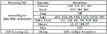
All the instructions are 32 bits long. There are total 27 instructions that have been implemented in the design. According to their purposes, the instructions can be divided into eight groups which are illustrated in table 1.
TABLE 1
INSTRUCTION SET OF PROPOSED PROCESSOR
A 32-bit instruction is encoded as follows. The most significant 4 bits represents the opcode (bit 31–bit 28).The next
5 bits represent the ALU operation (bit 27–bit 23), next 3 bits represent the destination or source register (bit 22-bit 20), second source register (bit 19- bit 17) and the first source register (bit 16–bit 14) respectively. Next two bits are kept for branch condition. It is not necessary that all the three registers will be used in every instruction. The 12 LSB bits is used as the address offset. When a new instruction is fetched from the instruction memory, for example an arithmetic operation -
ADD R1, R2, R3,
this will be encoded in the instruction memory in the following format:
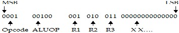
When this instruction comes to the controller and register file, the controller will interpret the opcode bits and will find that this is an add operation. The controller will output the corresponding control signals that set up the correct path for this operation. The register file will output the stored value for these corresponding registers. These data will be used as the source for the specified operations.
2.2 Hazard Handling
This design is modeled with a hazard free pipelined architecture which could handle two instructions simultaneously as it is a two stage pipelined processor. Since two instructions worked in parallel, the FSM is designed such a way that helped to detect any type of hazard and could control the data path to complete computation by solving the hazard. Hazard occurs when-
1. two load instructions are handled simultaneously
2. two instructions work with the same register content at a time (data hazard)
3. ALU is used for two instructions at a time
(structural hazard)
In this pipelined structure, the control unit is designed to solve the hazards and optimize speed. For the first
IJSER © 2012 http://www.ijser.org
International Journal Of Scientific & Engineering Research, Volume 3, Issue 7, July-2012 3
ISSN 2229-5518
and second type of hazards, the controller is designed for
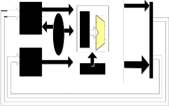
receiving the data direct from the internal data bus, which keeps the most recent data fetched from memory or stored value of accumulator register. By taking the value from internal data bus, the new data is bypassed before decode and execution stage from accumulator register. This improvement saves 1 cycle as this is not taken from the register bank which needs 1 more cycle to update with the corresponding value. Thus the calculation provides right result without any hazard. Fig 1 shows the bypassing technique of the proposed DSP processor.
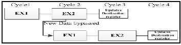
Fig 1 Bypassing technique for avoiding data hazard
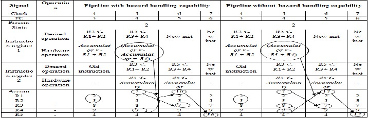
The improvement for hazard free FSM can be identified by the comparison of the pipelined architecture with and without hazard handling capability. Table 2 is used here to illustrate the comparison. For easier identification, some values (R1= 2, R2 = 5, R3= 8, R4= 9, R5= 4) are assumed for the instructions (R3 <- R1+ R2, R5 <- R3+ R4).
TABLE 2
COMPARISON TABLE BETWEEN PIPELINE WITH AND WITHOUT HAZARD HANDLING CAPABILITY
For the third type of hazard, a MUX is used instead of ALU, at the second stage of pipelining. The reason of using MUX for this modeling is to save ALU calculation from unwanted data, as a new instruction is using ALU at its first stage of calculation.
In this pipelined structure, the control signals generated by
the control unit are propagated down the pipeline synchronously with the system clock through pipeline registers. Besides, these control signals; there are two other types of control signals generated by the control unit. One is used for the memory read/write control signal and the other is used to control the ALU operation.
3 DATA PATH DESIGN
In this design, general purpose data path and dedicated mac unit follows the same method - pipelining. Some key components of the data path will be discussed in this paper including the ALU, multiply and accumulator (MAC) and memory design. To enhance the speed, data path is designed through pipelining.
3.1 ALU Design
The arithmetic logic unit (ALU) is an essential part of computer processor. It performs the arithmetic operations
(addition and subtraction) and logic operations (AND, OR, XOR etc.). The shifting and rotating tasks are also done through the ALU.
The design contains two 32-bit data inputs alu_in1 and alu_in2, and a carry output carryout. The five control inputs ALUOP0, ALUOP1, ALUOP2, ALUOP3, and ALUOP4 decide which operation should be executed. The outputs include a 32- bit arithmetic logic result and one of the three 1-bit flags (alu_out_pos: positive; alu_out_neg: negative; alu_out_zero: zero).
The most time consuming operations in ALU operation are
addition and subtraction [15]. In a ripple adder design, the adder propagates the carry from the lowest bit to the highest sequentially. Thus, the most significant bit of the sum must wait for the sequential evaluation of the previous thirty one (31) 1-bit adders, which creates large propagation delay. In theory, we can anticipate the carry input without waiting for it to be generated by the previous 1-bit adder component. This can be done by applying some calculations on the two operands and the carry input to the least significant bit of the adder. Delay for this kind of adder will be in order of log2N, where N is the bit number of the operands (32 in this case), instead of N as the usual ripple adder has [15]. Therefore, to increase the speed, a fast parallel adder, the Carry Look Ahead adder is used in this proposed design.
IJSER © 2012 http://www.ijser.org
International Journal Of Scientific & Engineering Research, Volume 3, Issue 7, July-2012 4
ISSN 2229-5518
3.2 Dedicated MAC Design
The proposed design contains a dedicated processing unit for multiply and accumulation. This design has implemented a 8 tap MAC. This MAC is dealing with sample values which are signed values. So the signed number is converted to unsigned number before it goes to the shift register file. As digital filtering operations needs only a single system clock cycle to perform the calculations, the corresponding MAC is modified to operate in one single cycle. The synthesis result of the single cycle operation is shown in Fig 2.
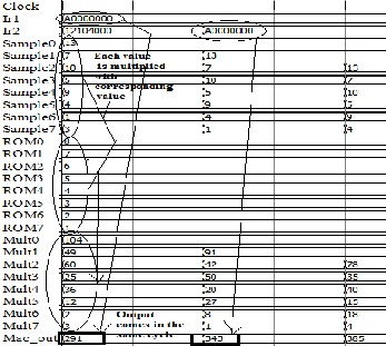
Fig 2 Simulation result of single cycle MAC
This is a dedicated processing unit for manipulating FIR filter operation. The MAC datapath is kept apart from the general purpose datapath where ALU is free from filtering task to deal with other instructions. For this two stage pipelined DSP processor, ALU needs 10 cycles to complete a two bit multiplication. The comparison between ALU and single cycle MAC is given below where the total required cycles are shown in table 3 to complete 2*2 multiplications.
TABLE 3
COMPARISON TABLE BETWEEN ALU AND MAC FOR EXECUTING
2*2 MULTIPLICATIONS
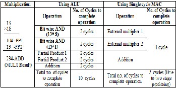
The benefit of using the external multiplier and accumulator (MAC) unit is to improve the speed. Since, in a
single cycle implementation of MAC, computations are done by a large number of hardware components in only one cycle, the duration of the clock cycle must be longer (twice) than the summation of all propagation delays of individual hardware components. To reduce the propagation delay, eight external multipliers are working parallelly which reduces clock period. This issue enhances speed of the processor which improves overall system performance.
Ideally, a traditional multiplier could be used here but n*n multiplication will give a result of 2n. This can increase the memory requirement and complexity. To overcome this, multiplier multiplies the lower 16-bit data from both operands. Thus, 16*16 multiplications will give result of 32 bits which eliminates complexity. Based on the timing analysis, the worst case delay of one multiplier is 23.764. Using one multiplier for overall calculation, the delay would be 23.764*8 = 190.112. By using eight traditional multipliers, the delay is now only 23.764 as all the multiplications are performed parallelly to compute the filter output. This improves the overall speed. Then all the multiplications results were added by a dedicated adder. Again flexibility is kept in this design where the MAC could either manipulate with four sample values or eight sample values. So four extra MUX were used to pass zero to the multiplier when number. of taps is four. This helped to eliminate invalid data from the filter value. To conduct parallel operations by the multipliers, it is required to receive all the sample valus simultaneously. To solve this problem. this design performs filtering operation only after all the shift registers are filled with sample values. The loadable eight shift registers are loaded with the previous register’s value. So the oldest data is lost each time.
3.3 FIR filter Design
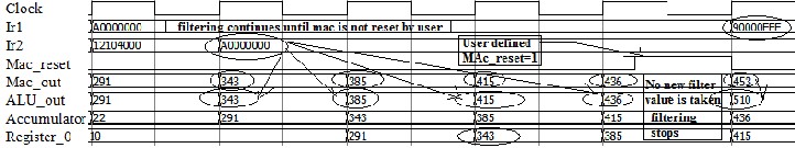
Finite Impulse Response (FIR) filter design task is the recurring technical task in the development of digital signal processing products and systems [16]. The digital filtering part of this processor is designed such a way so that it can perform continuous filtering until user stops the filtering. The sample program is shown in table 4 and functional simulation for FIR filter of this DSP processor is shown in Fig 3.
TABLE 4
THE SAMPLE PROGRAM FOR FIR FILTER OF PROPOSED DSP
PROCESSOR
It can be seen from this simulation that, at cycle-3 the FIR filter instruction is fetched and the EX1 stage started to operate. For this instruction, the external datapath or the special purpose datapath calculates the filter output. The output (here the values are- 232, 253) is passed through the
IJSER © 2012 http://www.ijser.org
International Journal Of Scientific & Engineering Research, Volume 3, Issue 7, July-2012 5
ISSN 2229-5518
ALU to the accumulator register. At next Active clock Edge, this filter output is loaded to the register file.
Fig 3 The functional simulation for FIR filter of proposed DSP processor
instruction memory and b) one for data memory. The
The FIR filtering is a continuous filtering of a real world signal. Thus the filter operation requires the information for stopping filtering. A user dependent signal Mac_reset is checked for this purpose. If the Mac_reset is found low then filtering is continued and no new instruction will be fetched. The simulation shows the next instruction fetched is a FIR filter instruction as user is not yet stopped filter operation
separation of memories allows no address conflicting between
the two memories by providing the ability of simultaneous memory access. Therefore, it is possible to improve the speed easily. Fig 4 illustrated the used Harvard architecture for the proposed design.
Data address
(Mac_reset = 0 at cycle 4). The reset signal is pressed before
cycle-5 which stops the filtering and fetches a new instruction.
After the reset signal is pressed, no filter output is loaded to the register which demonstrates the continuous filtering operation of the proposed DSP processor.
4 MEMORY DESIGN
Typical Von Neumann architecture has only one common memory which is used for either instruction fetch or data transfer [17]. The Von Neumann architecture uses only a single memory bus for both data memory and instruction memory. This is economical and simple to use because the
Program
Memory
Data Memory
32 bit instruction
C O N T R O L E R
32 bit Data
Pipelined
R datapath
E A
G D
A D
F L R I E L S E S
B U S
MAC
instructions or data can be located anywhere throughout the
available memory. Von Neumann architecture does not permit multiple memory accesses.
A reduced Cycle per Instructions (CPI) requires more than one memory access per clock cycle. With this memory architecture, reduced CPI cannot be achieved. For some instructions, it is necessary to access data memory once at most (e.g. LD, ST). To fetch the two operands in a single instruction cycle, we need to make two memory accesses simultaneously. Typical DSP operations require many additions and multiplications. The DSP processor needs to access both data and instruction memory simultaneously to perform the multiplication and addition faster. The two stage pipeline of the proposed processor is designed such a way that it requires both instruction and data operands simultaneously to perform an operation. To achieve faster memory accesses per instruction cycle this design follows Harvard architecture which has separate instruction and data memories. The utilization of normal Harvard architecture which has two separate physical memory buses, allows the proposed design to support two simultaneous memory accesses: a) one for
Fig 4 Used Harvard architecture for proposed design.
If we take a look in ARM7 pipelined processor which used Von Neumann architecture then we can see that the ARM7 has 2^20 = 1 M of the ROM address space and 2^19 = 512 k of the RAM address space in the same memory module [17]. The proposed design has 32 bit addressing both for data and instruction memory which allows the highest memory size to be 2^32 = 4GB for the design. Thus, the larger memory can be a benefit for faster processing. For this design, total memory usage is 93.896 megabytes.
For the safe design purpose or control over unwanted
memory output, a tristate buffer is used in the output of data memory. The purpose is to keep the data bus unconnected when it is not accessed by the processor. This helps to save the calculation from unwanted data.
5 PIPELINING AND DATA FORWARDING
The most important issue is to develop the design with two stage pipeline architecture. The pipelined structure is the heart of this design and responsible for speed optimization. In this design, both data paths include a single pipeline with two
IJSER © 2012 http://www.ijser.org
International Journal Of Scientific & Engineering Research, Volume 3, Issue 7, July-2012 6
ISSN 2229-5518
stages: Execution Stage1, Execution Stage2. In first cycle,
Execution stage1 (fetch, decode & execute) is performed.. Execution stage 2(Mem & WB) operates in the next clock cycle.
The primary reason for separating the stages is to keep the
system clock operates faster with less combinational delay. To enhance the speed, the general purpose data path is modified by adding some dedicated registers. For the load or store type operation, a special register is used which helped to complete any load or store type operation only in two clock cycles. All instructions of this processor can be executed within two clock cycles. All the stages of proposed processor were
synchronized with system clock. Fig 5 shows the two stage
pipelined diagram of the proposed processor.
For this pipelined architecture, the FSM is designed in a
manner to handle any instruction between two stages. The
processor utilizes highest 2 clock cycles for any instruction to complete with manipulation of hazard. A new instruction is fetched during each clock cycle.
The data forwarding method is used in the design when
two loads are dealing with same operand as destination and
source. Thus, the EX2 stage is moved to the front of the EX1 stage.
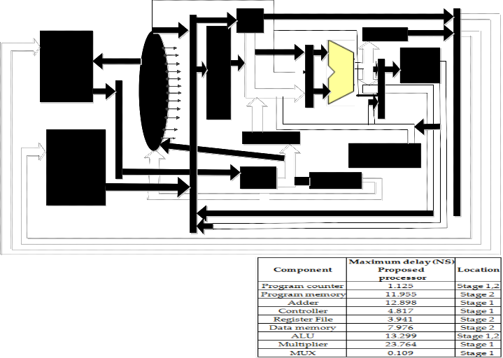
Fig 5 System diagram of Proposed 32 bit Pipelined DSP Processor
EX2(Mem & WB)
R
decode
PC
Instruction Address
execute
ADDRESS
Data address
Reg E
data G
I
EX1(ID)
REGISTER A
INSTRUCTION MEMORY
jump
C branch I S L O aluop1 N T U
E L
X U
E A O
EX1
E
ACCUMUL
ATOR
WB Alu_out
EX1(IF)
N aluop2 T E B
T Chip sele E R
C L U X
U U T E
REGISTER A
D
32 bit instruction
E X
Load U T
R S D
O op N F E U R
L mult A I 1 T E
E address L L
E
C R Immidi D
U ate data
E S
S
ALU bus
DATA MEMORY
accumulatorA T
E A
1 B
32 bit instructio U S
32 bit data
IMMIDIATE DATA
IR1 IR2
Ir2
B U
MAC S
(CO- PROCESSOR)
ALU OUT
6 PERFORMANCE ANALYSIS AND DISCUSSIONS
Performance gain of the proposed DSP processor is demonstrated through comparing among pipeline stages. Based on the timing specification from the synthesis result of each system building component, as shown in table 5, we get the execution time for all the instructions depending on different routes. It is clear from the table that timing specification which determines that execution time is almost equally distributed into all the pipeline stages.
TABLE 5
TIMING ANALYSIS AMONG PIPELINE STAGES By considering the worst case delays, the speed of the
processor is found around 13 MHz. The proposed design has implemented 27 instructions which requires 28 cycles to complete execution of all the instructions. Thus the throughput of proposed DSP processor= 27/(28* 80ns) = 12.06
MB/s.
IJSER © 2012 http://www.ijser.org
International Journal Of Scientific & Engineering Research, Volume 3, Issue 7, July-2012 7
ISSN 2229-5518
With pipelining we can improve the CPI by exploiting instruction level parallelism which helps to fetch 1 instruction in every cycle. As a result, two instructions are completed in two cycles in this two stage pipelined processor. With a single- issue processor, the best CPI attainable is 1 [18]. CPI of proposed processor is shown below, (assuming the program has 1 R-type instruction, 1 load instruction).
CLK 1 2 3
R EX1(IF,ID,EX) EX2(Mem,WB)
LD EX1(IF,ID,EX) EX2(Mem,WB) CPI of proposed DSP processor =2/2 = 1.
The reduced CPI is helpful for reducing cycle wastage and
improving clock rate. With a less CPI of 1, the performance
will be better in proposed design. To complete an individual instruction, the proposed processor takes two clock cycles (that is, it has two-cycle latency) [19]. This helps to gain higher processing speed in the new design.
The proposed design has an ability to handle the pipelined stages in parallel. This ability helps the processor to reduce the clock cycle and increases speed. The simultaneous memory access as well as write back strategy improved the performance without stalling when memory access is not available.
7 CONCLUSIONS AND FUTURE WORK
In this paper, a 32-bit two stage pipelined DSP processor is modeled. The complete system is defined in VHDL and simulated and tested using Modelsim 6.5. Each system building component is synthesized using the Xilinx 8.2i and then implemented on Xilinx Spartan-3E FPGA which proved to work properly. All the operations were verified with functional simulations which demonstrate that the FSM of this two stage pipelined DSP processor can successfully manipulate two instructions at a time even if they have hazards and produce correct cycle by cycle timing. To properly analyze the operations of this processor, each operation is checked with post fit simulation. This simulation successfully matches with the functional or behavioral simulation which validates the successful operation of the proposed DSP processor. Based on the synthesis result and timing evaluation of each system building components, the speed and throughput of the processor are found around 13
MHz and 12.06MB/sec respectively.
In future, the performance of this processor can be improved by further extending the number of pipeline stages and by providing support for floating point operations. The pipelining portion of the processor can be improved by increasing number of stages and by adding more high performance units to enhance the calculation speed.
REFERENCES
[1] M. E. A. Ibrahim, M. Rupp , and H.A. H. Fahmy, “Power Estimation
Methodology for VLIW Digital Signal Processors,” Proc. ACSSC, 2008.
[2] V. Gnatyuk and C. Runesson, “A Multimedia DSP processor design”, M.S. Thesis, Department of Electrical and Electronics, Linkoping University, Sweden, 2004.
[3] K. Karuri and R. Leupers, Application Analysis Tools for ASIP Design: Application Profiling and Instruction-set Customization, 1st ed., Springer, pp.
6-11, 2011.
[4] D. Skolnick and N. Levine, “An Introductory Course in DSP System Design,” Analog devices, http://www.analog.com/library/analogDialogue/archives/31-1/DSP.html.
1997
[5] “Xilinx Spartan-3 FPGA Family Data Sheet,” Product Specification
DS312, Xilinx, Calif, Nov. 2006.
[6] A Primer on FPGA-based DSP Applications, Trends, Options, Considerations, and Tools for Using Re-configurable FPGA Platforms as an Alternative to Dedicated DSP Hardware, White Paper, Acromag, Wixom, MI, May, 2008.
[7] D. Zaretsky, M. Mittal, T. Xiaoyong , P. Banerjee, “Overview of the FREEDOM compiler for mapping DSP software to FPGAs,” Proc. FCCM, p.37, 2004.
[8] I. Kuon and J. Rose, “Measuring the Gap Between FPGAs and ASICs,” IEEE Transactions on Computer-Aided Design of Integrated Circuits and Systems, vol. 26, no. 2, pp. 203-215, Feb. 2007, doi:
10.1109/TCAD.2006.884574.
[9] J. Cong, B. Xiao, “mrFPGA: A Novel FPGA Architecture withMemristor-Based Reconfiguration,” Proc. ACM International Symp. Nanoscale Architectures, pp. 1-8, July 2011,doi:
10.1109/NANOARCH.2011.5941476
[10] C.-J. Chou, S. M. krishnan and J. B. Evans, “FPGA implementation of
digital filters,” Proc. ICSPAT, 1993
[11] J. Becker, M. Glesner, “A Parallel Dynamically Reconfigurable Architecture Designed for Flexible Application-Tailored Hardware/Software Systems in Future Mobile Communication”, The Journal of Supercomputing, vol.19, no.1,pp. 105-127, May 2001.
[12] M. Ghosh, “Design and implementation of different multipliers using VHDL,” B.S. Thesis, Department of Electrical and Electronics, National Institute of Technology, Rourkela, India, 2007.
[13] K. Anand and S. Gupta, “Designing Of Customized Digital Signal Processor” B.T. Thesis, Department of Electrical and Electronics, Indian Institute of Technology, Delhi, 2007.
[14] Chattopadhyay, W. Ahmed, K. Karuri, D. Kammler, R. Leupers, G. Ascheid, H. Meyr, “Design Space Exploration of Partially Re-configurable Embedded Processors,” Proc. Design, Automation & Test in Europe Conference & Exhibition, p.319, 2007.
[15] C. Li, L. Xiao, Q. Yu, P. Gillard and R. Venkatesan, "Design of a
Pipelined DSP Processor - MUN DSP2000,"Proc. NECEC, 2000.
[16] J. Treichler, Retrieved from the Connexions., http://cnx.org/content/col10553/1.3/. 2009.
[17] A. N. Sloss, D. Symes and C. Wright, “ARM System Developer’s Guide
Designing and Optimizing System Software,” 1st ed., Morgan Kaufmann, pp.
9-14, 2004.
[18] M. R.S. Balpande, M.R.S. Keote, “Design of FPGA based Instruction Fetch & Decode Module of 32-bit RISC (MIPS) Processor,” Proc. ICCSNT, p. 409, 2011.
IJSER © 2012 http://www.ijser.org
International Journal Of Scientific & Engineering Research, Volume 3, Issue 7, July-2012 8
ISSN 2229-5518
[19] Altium PPC405A 32-bit RISC Processor, Product Specification Core Reference CR0156 (V 2.0), Altium, Shanghi, July 2006.
IJSER lb) 2012
htt p://www .'lser.ora