International Journal of Scientific & Engineering Research Volume 4, Issue 2, February-2013 1
ISSN 2229-5518
Ch.Venkateswra rao1 , S.S.Tulasiram2 , Arun Kumar Rath3
Abstract- hybrid H- bridge inverter. The proposed novel cascaded Hybrid H-bridge produces higher voltage levels with less number This paper presents a single-phase multistring Multi-level photovoltaic (PV) inverter topology for Micro grid-connected PV systems with a novel of devices. This will reduce the number of gate drives and protection circuits requirement, this inurn reduces the cost increase the reliability. Design Procedure for various components of single Hybrid H- bridge cell is given. A cascaded Grid connected PV topology is proposed. Finally a Matlab/Simulink based model is developed and simulation results are presented.
Keywords: PVCell, Hybridge H-bridge, Multi-lebel phovoltaic(PV) inverter, Matalab/Simulink, Micro grid-connected PV System;
—————————— ——————————
I.INTRODUCTION
natural quantity available, it has been spotlighted as the future energy sources of promising potentiality, due As the PV system is clean and large enough in the to the stable supply of the energy and alternative method of responding to the problem of the earth environment followed by the increase of the demand for the electric power supply. Solar- electric-energy demand has grown consistently by 20%–25% per annum over the past 20 years, which is mainly due to the decreasing costs and prices. This decline has been driven by the following: 1) an increasing efficiency of solar cells; 2) manufacturing-technology improvements; and 3) economies of scale [2]. A PV inverter, which is an important element in the PV system, is used to convert dc power from the solar modules into ac power to be fed into the grid. A general overview of different types of PV inverters is given in [3] and [4].
recent years many variations and combinations of these topologies have been reported, one of them is the cascaded H-bridge [7-10].
————————————————
1. Ch.Venkateswra rao Ph.D Scholar(EEE), JNTUK,Kakinada
India, chvr_4581@yahoo.co..in
2..S.S.Tulasiram Professor(EEE JNTUH,,Hyd ,India
3 .Arun Kumar Rath , Asst.Professor(EEE ) GIET,Gunupur
Odisha India, PH-09861751904, rpmarun@gmail.com
II .HIGH POWER CONVERTERS
CLASSIFICATIONS
In recent years, multilevel converters have shown some significant advantages over traditional two-level converters, especially for high power and high voltage applications. In addition to their superior output voltage quality, they can also reduce voltage stress across switching devices. Since the outputvoltages have multiple levels, lower dv/dt is achieved, which greatly alleviates electromagnetic interference problems due to high frequency switching. Over
the years most research work has focused on converters with three to five voltage levels, although topologies with very high number of voltage levels were also proposed. In general, the more voltage levels a converter has the less harmonic and better power quality it provides. However, the increase in converter complexity and number of switching devices is a major concern for multilevel converter. There are several topologies available, being the Neutral Point Clamped [5], Flying Capacitor [6] and Cascaded H bridge inverter [7] the most studied and used. In
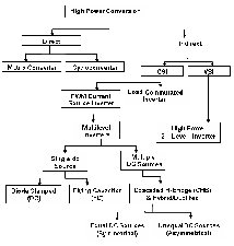
Figure 1 Classification of High power Converters
Fig.1 shows the classification of high power converters. Out of all converters Cascaded bridge configuration is more popular. Cascaded bridge configuration is again classified into 2 types 1) Cascaded Half Bridge 2) Cascaded Full
IJSER © 2013 http://www.ijser.org
International Journal of Scientific & Engineering Research Volume 4, Issue 2, February-2013 2
ISSN 2229-5518
Bridge or Cascaded H-Bridge. In this paper a novel cascaded hybrid H- Bridge topology is proposed for PV application.
A Half H-Bridge
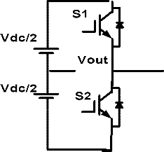
Figure 2 Half Bridge
Fig.2 shows the Half H-Bridge Configuration. By using single Half H-Bridge we can get 2 voltage levels. The switching table is given in Table 1
Table 1. Switching table for Half Bridge
Switches Turn ON | Voltage Level |
S2 | Vdc/2 |
S1 | -Vdc/2 |
B Full H-Bridge
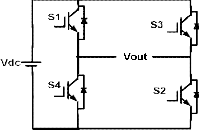
Figure. 3 Full H-Bridge
Fig.3 shows the Full H-Bridge Configuration. By using single H-Bridge we can get 3 voltage levels. The number output voltage levels of cascaded Full H-Bridge are given by 2n+1 and voltage step of each level is given by Vdc/n. Where n is number of H-bridges connected in cascaded. The switching table is given in Table2.
Table 2. Switching tabe Full Bridge
Switches Turn ON | Voltage Level |
S1,S2 | Vdc |
S3,S4 | -Vdc |
S4,D2 | 0 |
![]()
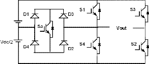
C Hybrid H-Bridge
Figure. 4 Hybrid H-Bridges
Fig. 4 shows the Hybrid H-Bridge configuration. By using single Hybrid H-Bridge we can get 5 voltage levels. The number output voltage levels of cascaded Hybrid H-Bridge are given by 4n+1 and voltage step of each level is given by Vdc/2n. Where n is number of H-bridges connected in cascaded. The switching table of Hybrid H-Bridge is given in Table 3.
Switches Turn On | Voltage Level |
Sa, S2 | Vdc/2 |
S1,S2 | Vdc |
S4,D2 | 0 |
Sa,S3 | -Vdc/2 |
S3,S4 | -Vdc |
Table 3. Switching table for Hybrid H-Bridge
D Cascaded Hybrid H-Bridge
IJSER © 2013 http://www.ijser.org
International Journal of Scientific & Engineering Research Volume 4, Issue 2, February-2013 3
ISSN 2229-5518
![]()
TI+ø
![]()
![]()
1 √2
S1 S3
D1 D3
iavg = 2TI
ø
I sin(ωt-ø)*(1 + k msinωt)dωt
Vdc/4
![]()
1 K m
Sa
Vdc/4
S4
D2
S2
Vout
![]()
![]()
= √2 I 2TI + 8 cos ø
The device RMS current can be written as![]()
i ms =
rr+ø 2 1
![]()
![]()
∫ 1 (√2 I sin(wt − ø))
∗ ∗ ((1 + k msinwt)dwt)
S5 S7
D5 D7
Vdc/4
Sb
ø zrr
![]()
![]()
=√2 I 1 +![]()
2
![]()
K m
3rr
cos ø
Vdc/4 S8 S6
D8 D6
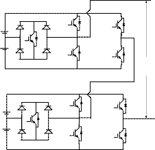
Figure 5. Cascaded Hybrid H-Bridges
The proposed CHHB uses less number of switches
B. IGBT Loss Calculation
IGBT loss can be calculated by the sum of switching loss and conduction loss. Where conduction loss can be calculated by,
to produce more voltage levels. This will reduce Gate![]()
Drivers and protection circuit requirement thus it reduce cost
Pon(IGBT) = Vceo ∗ Iavg(igbt) + Irms(igbt) ceo
1 m
and complexity of the circuit. For example for 9 level output the proposed converter uses 10 switches but cascaded H-![]()
![]()
![]()
Iavg(igbt) = √2 I [zrr + 8 cos ø]
Bridge converter uses 12 switches. This difference increases as the number of output voltage levels increases![]()
![]()
I = √2 I 1 + ![]()
m
3rr
cos ø
Table 4 Switching table for Cascaded Hybrid H-Bridge
Switches Turn On | Voltage Level |
Sa,S2,S8,D6 | Vdc/4 |
S1.S2,S8,D6 | 2Vdc/4 |
S1,S2,Sb,S6 | 3Vdc/4 |
S1,S2,S5,S6 | Vdc |
S4,D2,S8,D6 | 0 |
Sa,S3,S8,D6 | -Vdc/4 |
S3,S4,S8,D6 | -2Vdc/4 |
S3,S4,Sb,S7 | -3Vdc/4 |
S3,S4,S7,S8 | -Vdc |
III. DESIGN OF PROPOSED NOVEL HYBRID H- BRIDGE INVERTER
A. Device Current
The IGBT and DIODE currents can be obtained from the load current by multiplying with the corresponding duty cycles. Duty cycle, d =
½(1+Kmsinωt)
Where, m = modulation index K = +1 for IGBT, -1 for
Diode.![]()
iph = √2 I sin(wt − ø )
Where i = RMS value of the load (output) current,
Ø = Phase angle between load voltage and current.
Values of Vceo and rceo at any junction temperature can be
obtained from the output characteristics (Ic vs. Vce) of the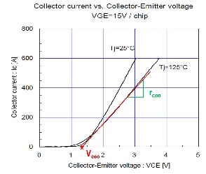
IGBT as shown in Fig .6.
Figure 6 IGBT output characteristics
The switching losses are the sum of all turn-on and turn-off energies at the switching events
Esw = Eon + Eoff = a + b I + c I2
Assuming the linear dependence, switching energy Esw =![]()
(a + b I + c I2 ) ∗ VDC
Then the device current can be written as follows.![]()
![]()
∴ idevice = √ I sin(wt − ø) ∗ (1 + km sin wt )
The average value of the device current over a cycle is
calculated as
Vnom
Here VDC is the actual DC-Link voltage and Vnom is the DC-
Link Voltage at which Esw is given. Switching losses are
calculated by summing up the switching energies.![]()
P = 1 ∑ E (i)
o
IJSER © 2013 http://www.ijser.org
International Journal of Scientific & Engineering Research Volume 4, Issue 2, February-2013 4
ISSN 2229-5518
Here ‘n’ depends on the switching frequency.
calculation gives the average junction temperatures. In order![]()
1 sw To
∑n(a + b I + c I2 )
to make the calculated values close to the actual values,![]()
![]()
![]() 1 a
1 a
To 2 +
![]()
b I
rr +
![]()
c Iz
4
transient temperature values are to be added to the average junction temperatures.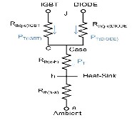
After considering the DC-Link voltage variations switching losses of the IGBT can be written as follows.
a b I
c I
![]()
VDC
![]()
Psw(IGBT) = sw
2 + rr +
∗
4 Vnom
So, the sum of conduction and switching losses gives the total losses.
PT(IGBT) = Pon(IGBT) + Psw(IGBT)
C. Diode Loss Calculation
The DIODE switching losses consists of its reverse recovery losses and the turn-on losses are negligible.
E ec = a + b I + c I2
Figure. 7 Thermal resistance equivalent circuit
a b I
c I
VDC
![]()
Psw(DIODE ) = sw
2 + rr +
∗
4 Vnom
![]()
The required capacitance for each cell depends
So, the sum of conduction and switching losses gives the total DIODE looses.
PT(DIODE ) = Pon(DIODE) + Psw(DIODE )
on the allowable ripple voltage and the load current. The rms
ripple current flowing into the capacitor can be written as follows and the ripple current frequency is double the load current frequency (Hybrid H-Bridge).
The total loss per one switch (IGBT+DIODE) is the sum of one IGBT and DIODE loss.
PT = PT (IGBT) + PT (DIODE)
S1
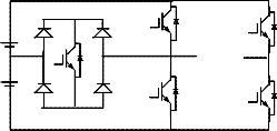
Vdc/2 D1 D3
Sa
Vdc/2
S3
Vout
D. Thermal Calculations
The junction temperatures of the IGBT
S4 S2
D4 D2
Figure. 8 Hybrid H-Bridge converter
and DIODE are calculated based on the device power losses
and thermal resistances. The thermal resistance equivalent![]()
I
Ic = − V
1
(|Uac | ∗ K + IwL) sin(2wt)
2
circuit for a module is shown in Fig 7. In this design the
thermal calculations are started with heat sink temperature as
the reference temperature. So, the case temperature from the
dc
Since the value of ‘L’ is very small, the above equation can
be written as below.
model can be written as follows.![]()
I
Ic = −![]()
dc
1
(|Uac | ∗ K) sin(2wt)
2
c = PT tt(cct) + t
Here Rth(c-h) = Thermal resistance between case and heat sink
IC = −K 1 |
m 2
Uac
Vdc
| ∗ sin(2wt)
PT = Total Power Loss (IGBT+DIODE)![]()
= −K
sin(2wt)
IGBT junction temperature is the sum of the case
temperature and temperature raise due to the power losses in the IGBT.
2
Here ‘m’ is the modulation index.
Here Icp = C
m ![]()
dupp
dt
(IGBT) = PT(IGBT) tt( cc)IGBT + c![]()
I √2 = C 2w ∗ ∆V Vdc
2
DIODE junction temperature is the sum of the case
temperature and temperature raise due to the power losses in
the DIODE.
junction temperatures. In order to make the calculated values close to the actual values,
(DIODE) = PT(DIODE ) tt( cc)DIODE + c
The above calculations are done based on the average power
losses computed over a cycle. So, the corresponding thermal![]()
![]()
m 1
C = 2 I
4w ∆V Vdc
IJSER © 2013 http://www.ijser.org
International Journal of Scientific & Engineering Research Volume 4, Issue 2, February-2013 5
ISSN 2229-5518
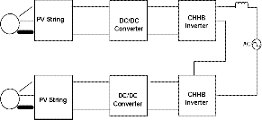
IV: PROPOSED PV SYSTEM 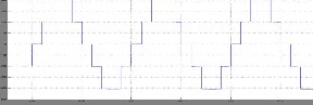
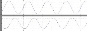
Figure12. Five level output of Hybrid H-bridge
Figure. 9. Grid Connected PV System
The general block diagram of PV system is shown here. The PV string converters solar radiation into DC.Here we are using DC/DC Boost converter to increase the output voltage. The output inverter converts DC into AC and feeding into the grid. The proposed system uses small PV array cascading to produce higher voltage output. This system reduces overall cost and complexity. The Fig.8 shows the proposed PV configuration.
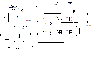
Fig. 10 Shows the Matlab/Simulink model of complete PV system. It consists of PV array block, DC/DC converter Block, Hybrid H-Bridge Block.
Figure. 10 Matlab/Simulink model of Hybrid H-bridge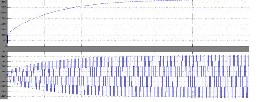
Fig. 11 shows the inverter input DC voltage and Multilevel AC output voltage. Fig. 12 Shows the five level output of the Hybrid H-Bridge. Fig.13 shows the grid voltage and current wave forms.
Figure.11 Inverter Input and Output
Figure13 Grid voltage and Grid current
This paper presents a single-phase multistring Multi-level photovoltaic (PV) inverter topology for grid- connected PV systems with a novel hybrid H- bridge inverter. The proposed novel cascaded Hybrid H-bridge produces higher voltage levels with less number of devices. This will reduce the number of gate drivers and protection circuits requirement, this inurn reduces the cost increase the reliability. Design Procedure for various components of single Hybrid H- bridge cell is given. A cascaded Grid connected PV topology is proposed. Finally a Matlab/Simulink based model is developed and simulation results are presented.
VII. REFERENCES
grid connected inverter for photovoltaic solar power generation system,” in Proc. IEEE PowerCon, Oct. 2002, vol. 1, pp. 570–573.
[2] J. M. Carrasco, L. G. Franquelo, J. T. Bialasiewicz, E. Galvan, R. C. PortilloGuisado, M. A. M. Prats, J. I. Leon, and N.Moreno-Alfonso,
“Power-electronic systems for the grid integration of renewable energy s[1] N. A. Rahim and S. Mekhilef,
“Implementation of three-phase ources: A survey,” IEEE Trans. Ind. Electron., vol. 53, no. 4, pp. 1002–1016, Aug.
2006.
[3] S. B. Kjaer, J. K. Pedersen, and F. Blaabjerg, “A review of single-phase grid connected inverters for photovoltaic modules,” IEEE Trans. Ind. Appl., vol. 41, no. 5, pp. 1292–
1306, Sep./Oct. 2005.
[4] S. Daher, J. Schmid, and F. L.M. Antunes, “Multilevel
inverter topologies for stand-alone PV systems,” IEEE Trans. Ind. Electron., vol. 55, no. 7, pp. 2703–2712, Jul.
2008.
[5] M. Meinhardt and G. Cramer, “Past, present and future of grid-connected photovoltaic- and hybrid-power-systems,” in Proc. IEEE-PES Summer Meeting, Jul. 2000, vol. 2, pp.
1283–1288.
[6] S. Kouro, J. Rebolledo, and J. Rodriguez, “Reduced
switching-frequency modulation algorithm for high-power multilevel inverters,” IEEE Trans.Ind. Electron., vol. 54, no.
5, pp. 2894–2901, Oct. 2007.
IJSER © 2013 http://www.ijser.org
International Journal of Scientific & Engineering Research Volume 4, Issue 2, February-2013 6
ISSN 2229-5518
[7] S. J. Park, F. S. Kang, M. H. Lee, and C. U. Kim, “A new single-phase five level PWM inverter employing a deadbeat control scheme,” IEEE Trans. Power Electron., vol. 18, no. 18, pp. 831–843, May 2003.
[8] L. M. Tolbert and T. G. Habetler, “Novel multilevel
inverter carrier-based PWM method,” IEEE Trans. Ind. Appl., vol. 35, no. 5, pp. 1098–1107, Sep./Oct. 1999.
[9] Y. Liu, H. Hong, and A. Q. Huang, “Real-time calculation of switching angles minimizing THD for multilevel inverters with step modulation,” IEEE Trans. Ind. Electron., vol. 56, no. 2, pp. 285–293, Feb. 2009.
[10] N. S. Choi, J. G. Cho, and G. H. Cho, “A general circuit topology of multilevel inverter,” in Proc. IEEE 22th Annu.
PESC, Jun. 24–27, 1991, pp. 96–103.
[9]L.M.Tolber, T.G.Habetler, “Novel Multilevel inverter Carrier based PWM Method,” IEEE Ind.Appli., vol.35. pp.1098-1107. Sep/Oct 1999.
[10]Holmes, D. G. and Lipo, T. A., Pulse width modulation for power converters: principles and practice, IEEE. [11]T.H.Barton, "Pulse Width Modulation Waveforms – The Bessel Approximatilon", IEEE-IAS Conference Record,
Authors Profile

Ch. Venkateswara Rao receieved his M.Tech degree from JNTUK, kakinada and U.G from IE (India), Kolkata) in the year 1993. A life member in ISTE and IAENG. This Author won first prize in Energy conservations Award for the year
2009. He is currently working as a professor in the department of EEE in
Gandhi Institute. of Engineering and Technology, Gunupur, Odisha He guidemany.UG & PG Projects. He is having overall Industrial &Teaching experience of 18 years. His major Research interests are Energy conservations and Smart Grids.
, S.S.Tulsiram working as a Professor in the Department of EEE in JNTUH Hyd. He has 30 years of Teaching experience. He is former Head of the department of EEE, JNTUCE, Kakinada. The Author has Published many papers in International & National Journals/ Conferences. His research interests are Power Systems, High Voltage Engineering & smart grid technology.
Arun Kumar Rath received his M. Tech Degree in Power Electronics and Drives from GIET, Gunupur under BPUT and UG from BPUT. A life time member of ISTE and also a life time member of SESI He is working as a Asst. professor in EEE Department at Gandhi institute of engineering & Technology. He is having more than 9 years Industrial and teaching experiences. His interest areas are Power
system engineering and Power Electronics & smart grids technology.
IJSER © 2013 http://www.ijser.org