International Journal of Scientific & Engineering Research, Volume 5, Issue 2, February-2014 154
ISSN 2229-5518
DIGITAL COMMUNICATION RECEIVER BASED ON FPGA DESIGN
Muthna Jasim Fadhil1
Abstract— In a digital communications systems where the data transferred in bit stream, the processing need to be very fast and more accuracy than that use in traditional circuits of digital communication system. FPGA package having these facilities so the receiver digital communication carried out in FPGA package for that reason. Research contained two parts; the first part implements digital communication receiver in FPGA package. The second part compare between actual traditional circuit (AICD) and FPGA.The system has been worked in high speed action and high accuracy when implemented in Xilinix-XC-95 FPGA Package and good results have been recorded.
Index Terms— FPGA package, receiver communications, synchronization system.
—————————— ——————————
1 Introduction
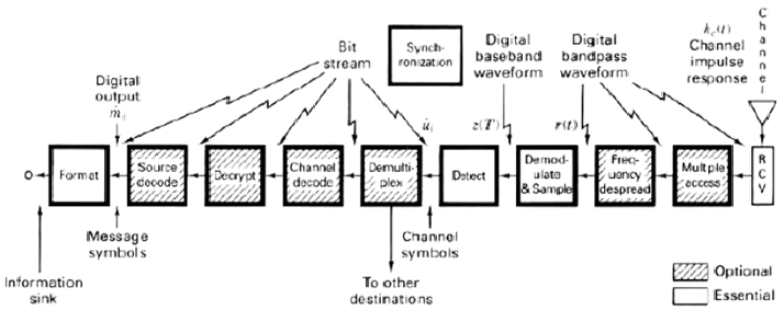
In a coherent receiver, synchronization is the most commonly used technique for recovering the sample functions from the received waveform. These sample functions are then used as reference signals for a correlator[5]. Synchronization-based receivers have advantages over non coherent ones in terms of noise Performance and bandwidth efficiency. These advantages are lost if synchronization cannot be maintained[2]. Many modern communications applications, such as mobile or indoor radio, are susceptible to multipath propagation effects arising from interaction between signals at the receiver which travel along different propagation paths. By contrast with a conventional digital modulation scheme, where the transmitted symbols are mapped to a finite set of periodic waveform segments[3]. Receiver digital communication system shown in fig.1. A principle difference between analog and digital communication systems has as to do
Fig.1: Receiver digital communication system
with the way in which we evaluate their Performance Analog systems draw their waveform from an infinite set, that is a receiver must deal with an infinite number of possible wave shapes[6] .The
————————————————
1Department of Electrical Power, Electrical and Electronics Technical Collage, Authority of Technical Education, Baghdad-Iraq. Mothanaali67@yahoo.com
figures of merit for the performance of analog systems are Signal to noise ratio, percent of distortion or expected mean square error between transmitted and received waveforms. 2-Digital communication system transmits signal that represent digits. These digits form a finite set or alphabet, and the set is known a priori to the receiver. The figure of merit for the performance of digital systems is :-probability of error[7] .
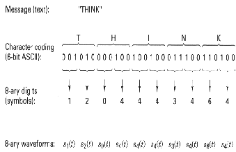
2 Messages, Characters and Symbols
Textual messages comprise a sequence of alphanumeric characters
. When digitally transmitted the characters are first encoded into a sequence of bits , called a bit stream or a baseband signal Groups of K bits can then be combined to form a new symbols . A system using a symbol set size of M is referred to as an m–ary system. The value of K or M represents an impotant initial choice in the
design of any digital communication system –Fig.2 shows example of messages , characters and symbol. The textual message in fig.2 is the word THIN,using 6 bit ASCII character coding ( American Standard Code for Information Intercharge
)forms a bit stream comprising (24)bit,where the symbol set size
M has chosen to be 8 then the bits are therefore partitioned into groups of three [K = log28=3] bits and forms symbol. The transmitter must generate 8 waveforms Si(t) , where i=0, 1 , 2
…..7 to represent each symbol [2]. The detection of band pass
signals employ the same concepts of baseband detection based on
IJSER © 2014 http://www.ijser.org
International Journal of Scientific & Engineering Research, Volume 5, Issue 2, February-2014 155
ISSN 2229-5518
realization of matched filter using correlator in the presence of
AWGN.The received signal is the sum of the transmitted reference
(prototype) signal plus a random noise
r(t)=Si(t)+n(t) (1) 0≤t≤T
The detection process consists of two basic steps:-
In the first step, the received waveform r(t), is reduced to a signal
Fig.4: Receiver digital communication system implemented and built in
Xilinix-XC-95 FPGA module.
comprised of M correlators, as shown in fig.3, that transforms a
received waveform, r(t),to a sequence of M numbers or correlator
output, Zi(T) (i=1,2,…M).Each correlator output is characterized by the following product integration or correlation with the received signal:
T
random variable Z(t) or to a set of random variables
Zi(T)[i=1,2,…M] formed at the
Z i (t)= ∫ r (t ).si(t )d (t )
0
(2) i=1,……..,M
Fig.2: Example of messages, characters and symbol sending by transmitter.
output of the demodulate or and sampler at time t=T, where T is the symbol duration.In the second step, a
Fig.4: Receiver digital communication system implemented and built in
Xilinix-XC-95 FPGA module.
symbol decision is made on the basis of comparing Z(T) to a threshold or on the basis of choosing the maximum Zi(T)[1]. Step1can be considered as transforming the waveform into a point in the decision space .This point can be referred to as pre detection point, the most critical point in the receiver[1].When we talk about received signal power, or received interfering noise on Eb/N , their values are always considered with reference to this pre detection point.The matched filter provides the maximum signal to noise ratio at the filter output at time t=T. Correlator is used to realization of a matched filter .We can define a correlation receiver
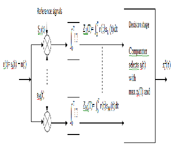
In the case of binary detection, the correlation receiver can be configured as a single matched filter or product integrated as shown in fig.3[4].with the reference signal being the difference between the prototype(reference) signals S1(t)-S2(t) The output of the correlator, Z(T) fed directly to the decision stage . The decision stage must decide which signal was transmitted by determining its location within single space and chooses the largest value of Zi(T)[3].
Fig.3: Demodulation and detection circuit
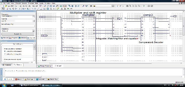
3 Circuit implementation in FPGA
IJSER © 2014 http://www.ijser.org
International Journal of Scientific & Engineering Research, Volume 5, Issue 2, February-2014 156
ISSN 2229-5518
It is clear that when carryout any circuit in FPGA we can get
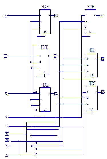
several advantages some of that: it can get high speed to transfer data and also reduce size of the circuit. Receiver digital communication system implements and builds in Xilinix -XC-95
FPGA as shown in fig.4. FPGA package consist from the
following components:-
1. Multiplier. 2. Integrator, matching filter and equalizer. 3.
Comparator and decoder.
3.1 Multiplier
Multiplier is the first part for receiver digital communication built
in Xilinix-XC-95 FPGA it has 12 IN- 6 OUT the function of this
item in order to make multiplication between receiving (original) signal Si (t) and noisy signal r(t) the internal design of multiplier are shown in fig.5. it contains from 6 AND gates and Shift register with 6 IN-6 OUT the purpose from shift register to shift instant data and receive next data the function of shift register in order to prevent mix and happen overlapping between instant and next data. The internal design of shift register are shown in fig.6 , it consist of 6 flip flop with One IN – One OUT where each flip flop shift one bit data.
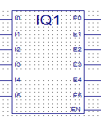
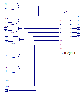 Fig.6: Internal design of shift register applied in FPGA.
Fig.5: internal design of multiplier applied in FPGA
3.2 Integrator , matched filter and equalizer
The detection of band pass signals employ the same concepts of
baseband detection based on realization of matched filter using
correlator in the presence of AWGN (additive white Gaussian noise). The matched filter provides the maximum signal to noise ratio at the filter output .Correlator is used to realization of a matched filter. the equalizer was used type transversal equalizers ,
it is Linear device that contain only feed forward elements Fig.7 shows the Integrator , matched filter and equalizer where all grouped in one item which is used in Xilinix-XC-95 FPGA package. It has 6 IN-6 OUT and one inhibit, where the inputreceived from multiplier and shift register and output send to comparator and decoder component.
Fig.7: Integrator , matched filter and equalizer structure in FPGA
3.3 Comparator and decoder
This component is the last stage in digital communication receiver the comparator use to take decision with hard limit either 1 or zero whither decoder use to transfer to digit number this item has 6 IN-
6 OUT it receive the input from Integ.,matched filter and equalizer and send the output to the output terminals which is mean the
IJSER © 2014 http://www.ijser.org
International Journal of Scientific & Engineering Research, Volume 5, Issue 2, February-2014 157
ISSN 2229-5518
output of FPGA. The internal design of comparator and decoder shown in fig.8.
Fig.8:Internal design of comparator and decoder circuit.
4 Simulation waveforms
After make simulation waveforms for the circuit of receiver digital communication system which is shown in fig.4 which is
Fig.9: Simulation waveforms for data input and output from Xilinix-XC-
95 package FPGA module
implemented and built in Xilinix-XC-95 FPGA module, we get
the waveforms diagram as shown in fig.9. Where the data transmitted and received Using 6 bit ASCII character coding
(American Standard Code for Information Interchange) forms a

International Journal of Scientific & Engineering Research, Volume 5, Issue 2, February-2014 158
ISSN 2229-5518
bit stream comprising transmitted and received (6)bit in one clock. It has been observed that from the 1st clock the 1st input data (111000) taking a period time start from inter to receiver channel after passing through multiplier, integrator, equalizer and matching filter finally passing through last stage comparator and decoder received in standard time(26ns) and in very high frequency about(38.461538 MHZ) ,the 1st data (111000) as explained by waveforms simulation in Xilinix-XC-95 FPGA Package fig.9. The above process repeated to 2nd data (010101)…etc and we got the same above results. While when sending these data by using traditional Actual Integrated Circuit Design (AICD) the processing for recei ving these data from input to output these circuits have frequency range (22.432 MHz – 33.7813 MHz) [2].
.
5 Probability of bit error for coherently detected binary PSK
If the carrier phase were reversed in a Binary Phase Shift Keying
(BPSK) modulation application, it would be effect on the message
the only effect would be an error in the bit during which inversion
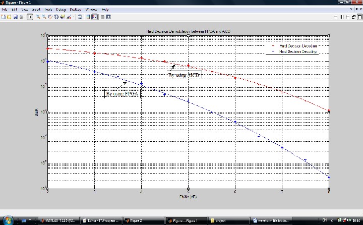
Fig.10: probability of bit error rate(BER) against bit energy to noise
spectral density ratio(E b /N 0 )
occurred or the bit just after inversion, since the message information is encoded in the similarity or difference between adjacent symbols. Sometimes messages (and their assigned waveforms) are differentially encoded and coherently detected simply to avoid these phase ambiguities. The simulation of the probability of bit error for coherently detected, binary decoded PSK against Eb /No for the circuit implemented in both FPGA package and AICD (Actual Integrated Circuit Design) as shown in Fig.10, it is clear in this figure that the probability of bit error rate(BER) against bit energy to noise spectral density ratio(E b /No )for circuit applied in FPGA are less than AICD. In Fig.10 above simulation in MATLAB It can be seen clearly that
the results for (BER) against (Eb /N0 ) for the circuit applied in Xilinix-XC-95 FPGA is better from the results if the circuit build in AICD.the above results are registered in table.1 below:
TABLE 1
BER against Eb/N 0 for circuit applied in AICD and FPGA:
IJSER © 2014 http://www.ijser.org
International Journal of Scientific & Engineering Research, Volume 5, Issue 2, February-2014 159
ISSN 2229-5518
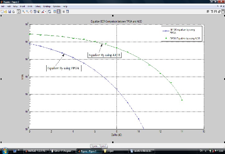
6 Decision feed forward equalizer (DFF):
A decision feed forward BPSK equalizer (DFF) is a linear
equalizer that uses previous detector decisions to eliminate the ISI (inter symbol interference) on the pulses that are currently being demodulated the decision feed forward equalizer(DFF) are applied in both AICD and FPGA package and we got the following results
as shown in fig.11.
Eb /N0 (dB) | BER AICD | BER FPGA |
0 | 0.5 | 0.82X10⁻¹ |
1 | 0.45 | 0.61X10⁻¹ |
3 | 0.33 | 0.34X10⁻¹ |
5 | 0.23 | 0.83X10⁻² |
7 | 0.81X10⁻¹ | 0.9X10⁻³ |
9 | 0.52X10⁻¹ | 0.63X10⁻⁴ |
10 | 1X10⁻² | 0.77X10⁻⁵ |
Fig 11: probability of bit error rate(BER) against bit energy to noise
spectral density ratio(E b / N 0 ) for equalizer applied
in both
FPGA
and AICD circuit.
In Fig.11 above the simulation in MATLAB It can be seen clearly that the results for BPSK equalizer for (BER) against (Eb /N0 ) for the circuit applied in Xilinix-XC-95 FPGA is better from the results of BPSK equalizer for the circuit applied in AICD.the above results are registered in table.2 below:
TABLE2
BER against Eb/N 0 for BPSK equalizer circuit applied in
AICD and FPGA.
7 Conclusions and results
IJSER © 2014 http://www.ijser.org
International Journal of Scientific & Engineering Research, Volume 5, Issue 2, February-2014 160
ISSN 2229-5518
1. For digital communication system the processing for receiving
data frequency for the circuit implemented in FPGA got frequency
38.461538 MHz is better from that frequency if implemented
circuit in AICD the frequency range (22.432 MHz – 33.7813
MHz) .
2. The probability of bit error rate (BER)for coherently detected, binary decoded BPSK against Eb /No for the circuit implemented in FPGA is better than the circuit implemented in AICD.
3. BPSK equalizer for (BER) against (Eb /N0 ) for the circuit applied in Xilinix-XC-95 FPGA is better from the results of BPSK equalizer for the circuit applied in AICD.
8 REFERENCES
[1] M. Hasler, “Engineering chaos for secure communication systems,” Phil. Trans. R. Soc. Lond. A, vol. 353, no. 1701, Oct. 16,
1995, pp. 115–126.
[2] B. Ramkumar. Automatic modulation classification for cognitive radios using cyclic feature detection. Circuits and Systems Magazine, IEEE, 9(2):27–45, 2009.
[3] S. S. Haykin, Communication Systems, 3rd ed. New York: Wiley,1994.
[4] S. Walters and T. Troudet, “Digital Phase-Locked Loop with
Jitter Bounded,” IEEE Transactions on Circuits and Systems, Vol
36, No. 7, July 1989.
[5] E. A. Lee and D. G. Messerschmitt, Digital Communications,
2nd ed. Boston, MA: Kluwer Academic, 1993.
[6] L. Zheng, D.N.C. Tse (2003). Diversity and multiplexing: A fundamental trade- o_ in multiple-antenna channels. IEEE Trans. Inform. Theory 49:1073-1096.
[7] A. Hottinen,M. Kuusela, K. Hugl, J. Zhang, B. Raghothaman (2006). Industrial embrace of smart antennas and MIMO. IEEE Wireless Communications 13:8-16.
IJSER © 2014 http://www.ijser.org