International Journal of Scientific & Engineering Research, Volume 4, Issue 12, December-2013 662
ISSN 2229-5518
DEVELOPING SHA-224/256 ALGORITHM DIGITAL SIGNATURE USING FPGA
V. VINAY KUMAR1, M. SAMPATH REDDY2, Dr. SYED MUSTHAK AHMED3
1,2,3 Department of ECE, SR Engineering College,Warangal, Andhra Pradesh,India
vinayvalusa@gmail.com1, mulasampathreddy@gmail.com2, syedmusthak_gce@rediffmail.com3
ABSTRACT : SHA (Secure Hash Algorithm) is a hash algorithm, the algorithm is collision-resistance and non-reversible, it is widely used in the information security field at present, which are more well-known SSL, IPSec and PKCS. Hash function is an important part of many crypto-algorithms, SHA-224 and SHA-256 are the two kinds of algorithms in the SHS standard (FIPS PUB 180-3). They can handle input messages whose length is less than 264 bits, but the outputs are separately compressed into 224 bits and 256 bits. This paper uses the similarity between SHA-224 and SHA-
256 algorithm and hardware description language to design and implement the time division multiplexing SHA-224/256 IP core. The IP core will not only be able to generate digital signature to protect the information integrity and security, but also generate the double-key of 3DES algorithm to provide a more reliable, safe, and
convenient keys. The IP core uses parallel structure and pipeline
224 bits and 256 bits. SHA-224 algorithm and SHA-256 algorithm have only two differences: first, the initialized hash values are different; second, the results of SHA-224are needed to be truncated.
technology to simplify the hardware design and improve the speed.
Keywords- Digital Signature; SHA-224/256; IP core; FPGA.
I. INTRODUCTION
SHS (Secure Hash Standard) is a hash algorithm (FIPS PUB
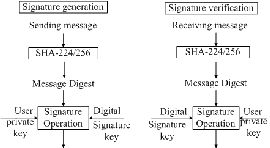
180-1), released by United States National Institute of Standards and Technology (NIST) in 1995. With the previous version (FIPS PUB 180-2 CHANGE NOTICE, August 2002), the biggest difference is that SHA-224 algorithm has been formally included in the SHS standard. Because SHS algorithm itself is a very complex algorithm, its calculation is to a larger quantity, and each iteration needs to rely on the previous calculation, it is often used hardware implementation to increase the processing speed. This project uses the similarity between SHA-224 and SHA-256 algorithm and hardware description language to design and implement the time division multiplexing SHA-224/256 IP core. The IP core will not only be able to generate digital signature to protect the information integrity and security, but also generate the double-key of 3DES algorithm to provide a more reliable, safe, and convenient keys. So it has a broad application prospects. A typical application of SHA in the digital signature algorithm is shown in Fig.1.
II. COMPUTER BUS MEMORY SYSTEM DESIGN
Figure 1 (a) Application Diagram of SHA-224/256 Digital
Signature (b) SHA 256 / 224 Hash Computation
SHA-256 algorithm has two steps to complete the calculation. The first step is to preprocess the input message to be filled and divided, generating 512 bits blocks. The second step is to calculate the hash value, that is to say, every block operates to produce the final results. After dividing blocks, every block messages can be processed by the following methods. And the details are described in reference [4].
1. Giving K0, K1 , …, K sixty-four 32-bits K the initial value.
2. Giving H0, H 1, H2 , H3, H4 , H5 , H6, Height 32-bits variables the specified initial hash values. Every block messages is to do the from step (3) to(7).
3. Divide the 512bits block into sixteen 32-bits words W0, W1 , …, W.
4. For i = 16 to 63
S0=ROTR7(Wi-15)
⊕ROTR18(W i-15) SHR3(Wi-15 )
7 19 10
SHA-224 and SHA-256 are the two kinds of algorithms in the
SHS standard. They can handle input messages whose length is
S1=ROTR (Wi-2 )⊕ROTR
Wi=Wi-16+S 0 +Wi-7 +S 1
(W i-2 )⊕SHR
(Wi-2 )
less than 264 bits, but the outputs are separately compressed into
IJSER © 2013 http://www.ijser.org
5. Initialize the hash value, a=H0, b=H1 , c=H 2 , d=H3 ,
e=H4, f=H 5, g= H6 , h=H7.
International Journal of Scientific & Engineering Research, Volume 4, Issue 12, December-2013 663
ISSN 2229-5518
6. For i=0 to 63
S0=ROTR2(a)⊕ROTR13(a) ⊕ROTR22(a)
maj=(a∧b) ⊕(a∧c) ⊕(b∧c)
t 2=S 0+maj
S1=ROTR6(e)⊕ROTR11(e) ⊕ROTR25(e) Ch=(e∧f) ⊕(﹁)e∧g)
t 1=h+S 1+Ch+K t +Wt
h=g, g=f, f=e, e=d+t1 , d=c, c=b, b=a, a=t 1+t
7. Add the hash values a, b, c, d, e, f, g, h respectively to the variables H0, H1, H2, H3, H4, H5 , H6 and H7.
8. Output 256-bits compressed code H0|| H1|| H2|| H3|| H4||
H5 || H6|| H7.
clock rising edge arrives to meet the iterative control. When input the corresponding data and control signal to the IP core, the IP core does iterative processing in a block (512 bits).
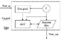
Figure 2 : IP Core Architecture
The counter is cleared after every 64 clocks to maintain synchronization between itself and the word. Its data flow is the
The signs ∧ , ⊕, ﹁ , + respectively represents bitwise AND,
following: Data pool gives Wt
and Kt
under the control of the
XOR, NOT and 32-bits addition operation. and ROTRm(Wn) represents that Wn rotates right m bits, SHRp (Wq) represents that Wq rotates right p bits. The sign | represents bitwise connect.
The first step can be achieved by the upper software. Therefore, several issues need to be solved for the calculation of hash values.
1. The multiplexing of IP core, a group of registers is used
to achieve the time-division multiplexing of SHA-224
Counter and sends them to ALU. ALU does the corresponding arithmetic and logic operations after receiving the data, and save the results to register files until the end of this iteration. At the beginning, the blocks, the words and the end, the Register files you need to provide the corresponding results for ALU or the output bus under the control of external control signals and the Counter
A. Data pool
IJSER
and SHA-256 algorithms.
2. Performance and area optimization, pipelining and parallel computing architecture will be used to design simple structure and fast IP core.
3. Determine the data bus width. Because the message length handled by the algorithm is variable, the external data bus width and the corresponding control core. From the third step and sixth step of the algorithm, the relationship between production and consumption among them entirely can be handled by the parallel architecture.
III. SYSTEM DEVELOPMENT
Every sub-module of the entire IP core is designed according to the data flow of the SHA-256 algorithm. First, determine the interfaces of the IP core. Considering the portability of the IP core,
32-bits data bus and 11-bits control bus. Control bus includes clock
signal, reset signal, control enable signal, function selection signal, control signal and state signal. Next, According the relationship between production and consumption of data flow, the IP core can be divided into the Data pool, ALU(Arithmetic Logic Unit), Register files and Counter four parts(shown in Fig.2). Data pool is used to save the constant and Wt in the algorithm, including the initial hash value, key value, and the values of the input words and the expansion words. ALU is used to complete the arithmetic and logic operations. Register files are used as the dedicated registers to
t save the values of a,b,c,d,e,f,g,h. Counter is added 1 in every
The Data pool consists of look-up table unit and shift register
unit. Look-up table unit is responsible for looking up the key value of this iteration according to the counter value. Shift register unit is responsible for completing the expansion from 16 words to 64 words. There is sixteen 32-bits registers, respectively recorded as W0 ,W…, W14, Wt. When each 512-bits block is processed, these registers assign and flow according to the counter value.
B. ALU
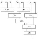
In the processing every word, logical operations in the every iteration may be a simple combination circuit, while the arithmetic only needs 32 bits adder to complete. From the description of the algorithm, calculating ‘a’ value is the longest path (It has five additions). So CSA (Carry Save Adder) of the parallel structure is used to reduce the carry signal delay[5][6] brought by the number of additions in order to improve the entire IP core speed. Due to every summand is also the intermediate result of the logical operation, it is as the input of the second level CSA. And the final calculation results are given by the CPA (Carry-Propagate Adder). The addition structure of ‘a’ value is shown in Figure.3
IJSER © 2013 http://www.ijser.org
International Journal of Scientific & Engineering Research, Volume 4, Issue 12, December-2013 664
ISSN 2229-5518
Figure 3. The Addition Structure of ‘a’ Value
IV. SYNTHESIS AND SIMULATION
In this design, this IP core is described by Verilog HDL language and has been implemented to Xilinx 8.1i. Finally it is simulated by ModelSim [7] to test if the IP core is correct.
A. Synthesis results:
The internal structure of FPGA, using the Hard Copy technology [8] turns the IP core to ASIC achieving that the power consumption will be further reduced and the performance and speed will be increased by almost 50% [9]
B. Timing simulation
Under that the simulation clock is 100MHz, its simulation waveforms are shown in Figure 4 (SHA-224) and Figure 5 (SHA-
256),
SHA-224
Let the Input Message Length is:200
Hash Length is: 224
Message Input:
11111111112222234444446666666788997ADC122200000000
HASH Code is:
V. CONCLUSION
This paper uses the similarity between SHA-224 and SHA-
256 algorithms to design a time division multiplexing IP core. 32- bits data bus makes this design has a friendly data interface, and the whole design has a simple hardware structure and fast running speed and can be widely used in digital signatures and 3DES key generation systems.
REFERENCES
[1] Wang Xiaoyun, Yu Hongbo and Yiqun Lisa Yin, Efficient
Collision Search Attacks on SHA-0[C], CRYPTO 2005[2]
[2] Wang Xiaoyun, Yiqun Lisa Yin and Yu Hongbo, Finding
Collisions in the Full SHA-1[C], CRYPTO 2005[3]
[3] Huang Chun, Bai Guoqiang, Chen Hongyi. Fast Implementation of the hardware structure of SHA-1 algorithm[J]. Journal of Tsinghua University 2005(45)1, pp.:123-125.
[4] FIPS PUB 180-3, Secure Hash Standard[S], National Institute
of Standards and Technology (NIST), 2008.
[5] Jian Honglun. Proficient VerilogHDL: The example
IJSER
BB67F6CF6B8D691556386954F3141CD13225F7DBFS41080919
B92167
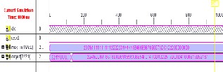
Figure 4. The Simulation Result of SHA-224
SHA-256
Let the Input Message Length is:400
Hash Length is:256
Message Input:
11111111112222234444446666666788997ADC12220000000011
111111112222234444446666666788997ADC122200000000
HASH Code is:
FEF36B3C4FBC52EE150AD59FE4049D741B58005C624743C36
4A857ADB
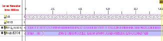
Figure 5. The Simulation Result of SHA-256
explanation of IC design core technology[M]. Electronics
Industry Press, 2005.
[6] Yang Xiaohui, Dai Zibin. FPGA-based implementation of
SHA-256 algorithm[J], Microcomputer Information, 2006(22)
4-2, pp.146-148.
[7] Jiang Hao, Li Zheying. FPGA design flow based on a variety of EDA tools [J], Microcomputer Information, 2007(23) 11-2, pp.:201-203
[8] Hard Copy II Device Handbook, Volume2 [OL], http://www.altera.com.cn/literature/hb/hardcopyii/hc_h5v2.pd f.
[9] IC Technology Seminar. FPGA modular design and Altera Hard Copy II structured ASIC[J], World Electronic Components, 2007,6, pp.:38-42
IJSER © 2013 http://www.ijser.org