International Journal of Scientific & Engineering Research, Volume 3, Issue 6, June-2012 1
ISSN 2229-5518
Comb Line Notch Filter Design on Silicon
Coplanar Transmission Line
Buddhadev Pradhan , Bhaskar Gupta
Abstract - A comb line notch filter is presented, in which two quarter wave length resonators are placed face to face on the signal line of a CPW. The CPW is designed on silicon substrate enabling compatibility with planar IC technology. The comb line notch filter rejection frequency is 12.75GHz, where the return loss -1.7dB and insertion loss is -3.8dB.This proposed structure is simulated using ANSOFT HFSS v13®.
Keywords – Comb line, notch filter, coplanar technology, CMOS technology, RF characterization.
————————————————————
Microwave filters are critical components for electronic warfare, radar, and communications systems. But typical filters are bulky, expensive, and consume large amounts of power [1]. Under such circumstances, we have proposed a comb line filter equipped with two quarter-wavelength simple resonators[4]. This filter had such a structure that the resonators are placed face-to-face on signal line of a CPW transmission line, leading to tight coupling between these resonators. This feature gave great advantages to this filter that any additional lumped elements were not needed to enhance the coupling.![]()
![]() Buddhadev Pradhan
Buddhadev Pradhan
IC Design and Fabrication Center,
Department of Electronics and Telecommunication
Engineering, Jadavpur University,
Kolkata: 700032, West Bengal , India
pradhanbuddha123@gmail.com
![]() Bhaskar Gupta
Bhaskar Gupta
Department of Electronics and Tele-communication
Engineering, Jadavpur University,
Kolkata: 700032 ,West Bengal, India
gupta_bh@yahoo.com
As comb line can be implemented by planar IC technology
[4], an added advantage of CMOS compatibility along with
low loss, high power and reduced size may also be
achieved. In this paper, we present a comb line embedded CPW transmission line on silicon substrate. To the best of our knowledge, no such design has been carried out on silicon substrate to allow CMOS compatibility at such high frequency ranges.
The comb line is etched on the signal strip of the CPW which enables the structure to behave as a notch filter, that reject only 12.75GHz fr equency. The proposed structure is simulated using ANSOFT HFSS v13®. We also suggest an equivalent circuit model of a comb line filter, which not only provides an insight into the system but also helps in its optimization.
II. PROPOSED DEVICE STRUCTURE
Figs.1(a) and 1(b) illustrate the top view and cross section of a comb line notch filter embedded CPW transmission line. A CPW configuration corresponding to W/S/W of 60/100/60 is chosen to obtain 50ohm characteristic impedance. The comb line quarter- wavelength resonators are patterned on the CPW central line which is housed on an oxidized high resistivity silicon substrate whose relative permittivity is 11.9 , thickness is
275µm and width & length are 820µm and 4000µm
respectively.
The CPW transmission line is made of Au (1μm thick) with
loaded comb line structure. The length and width of the comb line quarter wavelength resonators are given by L,T and c,d respectively and the gap between two quarter wavelength resonator is b.
IJSER © 2012
International Journal of Scientific & Engineering Research, Volume 3, Issue 6, June-2012 2
ISSN 2229-5518
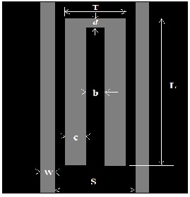
Fig. 1(a): Top view of a comb line structure loaded CPW
transmission line.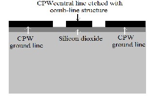
Fig. 1(b): Cross sectional view of the comb line structure loaded
lumped capacitors and Yc is the characteristic admittance of the distributed inductor modelling the coupling between resonators.
Yr =1/jωLr ----------------------- (1) Yc =1/jωLc ---------------------- (2)
As shown, the filter is made up of two identical transmission-line segments shortened to ground in one extreme and terminated in a lumped capacitor at the opposite end. The line-capacitor combination corresponds to the filter resonator, modelled as a parallel connection of the corresponding capacitor and the equivalent distributed inductor of the transmission-line segment. The coupling between the resonator lines is inductive, and is approximated as a series distributed inductor connecting the resonators. A distributed inductor refers to a transmission line shortened at one extreme, exhibiting an equivalent admittance [5]
Yeq= Y0 / tanθ ---------------------------(3)
where Y0 is the characteristic admittance
θ =(2πl√εeff /c)f --------------------------- (4)
where θ is the electrical length of the line.
This design starts by selecting a suitable CPW for obtaining 50ohm characteristic impedance (Z0). Here we report a single rectangular shaped comb line resonator etched onto the signal line of the CPW. The length of the comb line resonator (L) is very crucial for obtaining proper filtering actions. For a center rejection frequency of 12.75
GHz it is seen that the length of the resonator (L) would be
around 2000µm according to,
L =λg/4 -------------------- (5)
CPW transmission line.
III. PROPOSED DEVICE DESIGN
The schematic diagram of a comb line filter and CPW loaded transmission-line equivalent-circuit network is given in Figs.2(a)&(b),where Yr is the characteristic admittance of the lines, Cr is the capacitance value of the
where λg is the guided wavelength and is given by
λg =λ0 /√εeff ----------------------------- (6)
where εeff is the effective permittivity and is approximately given by
εeff =(εr+1) /2-------------------- (7)
IJSER © 2012
International Journal of Scientific & Engineering Research, Volume 3, Issue 6, June-2012 3
ISSN 2229-5518
where εr is the relative permittivity of the substrate which is
11.9 for silicon.
RF Characterization :-
The choice of the dimensions for the comb line resonators is very crucial for obtaining the desired performance. As already discussed the length & width of the comb line resonator are chosen as 2000µm and 80µm.Varying the comb line resonator width (‘c’ & ‘d’) we observed the rejection notch frequency. This has been validated with the help of the proposed model and FEM simulation using ANSOFT- HFSS v13®. Figs. 3(a) & (b) show the simulated S-parameters for the Comb line notch filter with varying
‘c’ & ‘d’ .These simulation results show very good rejection around -32 dB when c=20µm & d=30µm. Fig.4 shows the result for S-parameters comb line filter for the optimal case of c=20 µm and d=30 µm. High rejection for the optimal notch filter is shown at 12.75 GHz notch frequency with a return loss of around -1.7dB .
diagram .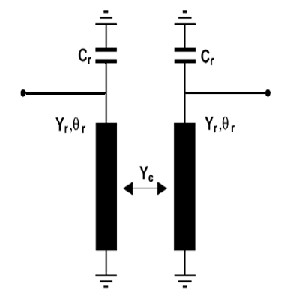
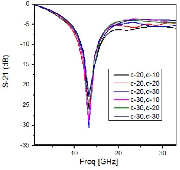
Fig.2.(a) Comb line filter schematic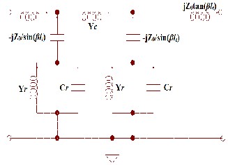
Fig.2.(b).Comb line filter CPW loaded transmission-line
equivalent circuit network.
.
Fig. 3.(a) comb line notch filter HFSS-simulation
S-21 result for
The proposed device structure has been simulated using standard FEM tools and the results are discussed in the following section.
IV. RESULTS AND DISCUSSIONS
width-‘c’ & ‘d’.
variation of comb-line resonators
IJSER © 2012
International Journal of Scientific & Engineering Research, Volume 3, Issue 6, June-2012 4
ISSN 2229-5518
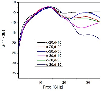
Fig.3.(b) comb line notch filter HFSS-simulation
S-11 result for variation of comb-line resonators width-‘c’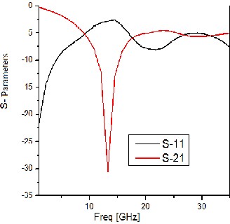
& ‘d’.
Fig.4. comb line notch filter HFSS-simulation results for
variation of resonator width c=20,d=30
V. CONCLUSIONS
In this paper, we propose a comb line notch filter as the first demonstration of using planer IC technology on silicon
substrate.With its high rejection frequency and compact size, this filter is promising for applications in microwave communications and radars. Further work is going on to improve the loss performance. Work is also in progress to achieve tuneability in the filter by using MEMS bridge.
ACKNOWLEDGEMENT
The authors would like to acknowledge the National Programme on Micro and Smart Systems(NPMASS) for providing the necessary support. Mr.Buddhadev Pradhan would like to acknowledge the support and guidance of Prof. Bhaskar Gupta, Dept. of ETCE, Jadavpur University.
REFERENCES
1. Vincze, A.D. ‘Practical design approach to microstrip combline filters’,IEEE Trans. Microw. Theory Tech., 1974, 22, pp. 1171–1181.
2. Brown, E.R.: “RF-MEMS switches for reconfigurable
integrated Circuits”, IEEE Trans. Microw. Theory Tech.,
1998, 46, pp. 1868–1880.
3 .Gabriel M. Rebeiz, ‚RF MEMS: Theory, Design, and
Technology”, John Wiley & Sons Ltd, Chapters 1, 9 and
10, pp.1-20, 259-324, 2003.
4. YASUSHI HORII Faculty of Informatics, Kansai
University 2-1-1 Ryozenji-cho, Takatsuki-shi, Osaka 569-
1095 Japan, TOSHIAKI KITAMURA, MASAHIRO
GESHIRO, SHINNOSUKE SAWA Osaka Prefecture
University 1-1 Gakuen-cho, Sakai-shi, Osaka 599-853 1
Japan . “MULTISTAGE DUAL-PLANE COMB-LINE FILTER
EXCITED BY CONDUCTOR-BACKED COPLANAR
WAVEGUIDE.”
5. Manuel Sánchez-Renedo, Roberto Gómez-García, Student
Member, IEEE, José I. Alonso, Member, IEEE, and César
Briso-Rodríguez “Tunable Combline Filter With Continuous
Control of Center Frequency and Bandwidth.”
6. Isak Reines,Andrew Brown, Mohammed El-Tanani, Alex Grichener and Gabriel Rebeiz, ‚1.6-2.4 GHz RF MEMS 3- Pole Suspended Combline Filter”, University of California San DiegoLa Jolla, Ca 92121 A. Brown Design
46055 Bloomcrest Dr. Northville, MI 48167.
7. K. Hirano, S. Nishimura, and S. K. Mitra, ‚Design of digital notch filters,” IEEE Trans. Circuits Syst., vol. CAS-21, pp. 540–546, July 1974.
IJSER © 2012
International Journal of Scientific & Engineering Research, Volume 3, Issue 6, June-2012 5
ISSN 2229-5518
8. I. C. Hunter et al., ‚Microwave filters—Applications and technology,” IEEE Trans. Microw. Theory Tech., vol. 50, no. 3, pp. 794–805, Mar. 2002.
9. T. Ishizaki, T. Uwano, and H. Miyake, ‚An extended configuration of a stepped impedance comb-line filter,” IEICE Trans. Electron., vol. E79-C, no. 5, pp. 671–678, May 1996
10. M. Sagawa, M. Makimoto, and S. Yamashita, “Geometrical structures and fundamental characteristics of microwave stepped-impedance resonators,” IEEE Trans. Microwave Theory Tech., vol. 45, pp. 1078–1085,
July 1997.
11. Tian-Hu Yu, S.K. Mitra and H. Babic, ‛Design of Linear Phase FIR Notch Filters‛, Sadhana, Vol. 15, Iss.3, pp. 133-55, Nov. 1990, India
12. S. J. Park, K. Y. Lee, and G. M. Rebeiz, ‚Low-loss 5.15–
5.70 GHz RF filter for wireless LAN applications,‛ IEEE
Trans. Microw. Theory Tech., vol. 54, no. 11, pp. 3931–3939, Nov. 2006.
IJSER © 2012