Fig. 1 classification of PCB inspection techniques.
International Journal of Scientific & Engineering Research, Volume 5, Issue 7, July-2014 1095
ISSN 2229-5518
Automatic Optical Inspection for PCB Manufacturing: a Survey
Eid M. Taha, E. Emary, Khalid Moustafa
In this survey, algorithms and techniques for the automated inspection of printed circuit boards are examined. A classification of these algorithms is presented and the algorithms are grouped according to this classification. This survey concentrates mainly on image analysis and fault detection techniques; these also include state-of-the-art algorithms.
utomated Optical Inspection (AOI) inspects a wide range of products, such as Printed Circuit Boards (PCBs), Liquid Crystal Displays (LCDs), transistors, automotive parts, lids and labels on product packages or agricultural products (seed corn or fruits). In case of PCB- inspection, a camera autonomously scans the device under test (DUT) for variety of surface feature defects such as scratches, stains, open circuits, short circuits and thinning of the solder as well as missing components, incorrect
components, and incorrectly placed components.
A machine vision or an AOI system can acquire millions of data points (pixels) in a fraction of a second. These data points are used for visual inspection and precision measurement.
AOI visually scans the surface of the PCB. The board is lit by several light sources and observed by a scanner or by a number of high definition cameras. This enables the monitoring of all areas of the board, even those hidden in one direction by other components. It should be noted that each manufacturer of AOI systems utilizes different inspection algorithms and lighting techniques, each of these systems may have varying strengths and weaknesses depending upon the item/product it inspect.
Assembly of Printed Circuit Boards (PCBs) using Surface
————————————————
• Eid M. Taha, Information Technology Dept, Faculty of Computers & Information, Cairo University, Egypt, E-mail: eidmahmoud@gmail.com
• E. Emary, Information Technology Dept, Faculty of Computers &
Information, Cairo University, Egypt, E-mail: e.emary@fci-cu.edu.eg
• Khalid Moustafa, Information Technology Dept, Faculty of Computers &
Information, Cairo University, Egypt, E-mail: k.moustafa@fci-cu.edu.eg
Mount Technology (SMT) has been widely used in the electronic industry recently. As a result, the electronic components rely on the solder joint to provide the electrical connection to the PCBs; therefore, the quality of the solder joint can be critical to the quality of the electronic components [1]. Automatic Optical Inspection (AOI) of solder joints has been a critical issue for quality control in PCB assembly as AOI has the enormous potential of completely automating human visual inspection procedures [2, 3].
In general, PCB inspection can be divided into three categories: reference comparison approach, design rule checking (non-referential) approach, and hybrid approach [6].
The reference comparison approach is based on a comparison between the image of the PCB to be tested and that of an ideal PCB which is conform to pre-defined design specifications. While it is a fast method for comparison and doesn't require any CAD data but any miss-orientation of a board’s placement may lead to wrong analysis in reference- based method [5]. There are two major techniques: image comparison methods and model-based inspection. Image comparison, which is the simplest approach, consists of comparing both images pixel-by-pixel using simple logic operators such as XOR. The main difficulty found in these techniques is determining a precise alignment of the reference image and the test image, which makes its utilization difficult. More sophisticated proposals under the same idea, involve feature and template matching [23], but suffer from the same problem and normally require a large number of templates. Model-based methods are techniques, which match the pattern under inspection with a set of predefined models. They are also called Graph-Matching Methods [23] and are based on the structural, topological, and geometrical properties of the image. The major difficulty
IJSER © 2014 http://www.ijser.org
International Journal of Scientific & Engineering Research, Volume 5, Issue 7, July-2014 1096
ISSN 2229-5518
of those methods is related to the matching complexity. Although Sun and Tsai [Sun and Tsai, 1992] proposed a technique called Pattern Attributed Hyper graph to make the method more practical, it still remains a complex and time- consuming method.
The design rule checking approach is based on the verification of the general design rules that is essential in the verification of the widths of conductors and insulators. As a kind of automatic inspection algorithm for bare PCB, the design rule checking has been proposed and well known to the automatic visual inspection system manufacturers [25]. The design rule checking (DRC) method checks if all patterns and spaces of PCB surface meet or violate common knowledge, which is called the design rule. Because a simple algorithm is applied directly to an image, the implementation of this algorithm is comparatively easy. This means that it does not require severe alignment and adjustment of a mechanical part to get a non-distorted image and can be easily parallelized. However, this method is a very time consuming process and a great computing power is needed to meet user’s requirement of inspection time.
Hybrid approach merges the advantages of the reference comparison method and the DRC method to overcome the weaknesses of each method. For example, most of the design-rule verification methods are limited to verifying minimum conductor trace, angular errors, and spurious copper. PCB defects which do not violate the design rules are detected by reference comparison methods. These methods can detect missing features or extraneous features. The design rule process detects most type of defects within small and medium features while the comparison methods are sensitive to the largest features. Hybrid approach makes use both of these methods as they complement each other and therefore achieve a high sensitivity of PCB inspection. Another way of classification is Front End and Back End [36] processing. When a computer vision system is proposed for the automatic detection, localization, and segmentation of solder joints on PCBs under different illumination conditions. This is referred to as the “front-end” inspection system. The back-end involves the classification of the solder joints. The front-end inspection system includes illumination normalization which is applied to an image to effectively and efficiently eliminate the effect of uneven illumination while keeping the properties of the processed image the same as in the corresponding image under normal lighting condition. Consequently special lighting and instrumental setup can be reduced in order to detect solder joints.
Table 1 explores most PCB error both for Bare PCBs [35] and
PCBs with SMT components.
TABLE 1, PCB ERRORS CLASSIFICATION
2 Shorts/bridges | ||
3 Missing conductor | ||
4 Missing Component | ||
5 Component with wrong polarities or flipped components | ||
6 Wrong Component Placed | ||
7 Incorrect hole dimension | ||
8 Missing hole | ||
POTENTIAL | 9 Partial Open | 9.1 Mouse bit |
POTENTIAL | 9 Partial Open | 9.2 Nicks |
POTENTIAL | 9 Partial Open | 9.3 Pinholes |
POTENTIAL | 10 Excessive spurious | 10.1 Specks |
POTENTIAL | 10 Excessive spurious | 10.2 Spurs/protrusions |
POTENTIAL | 10 Excessive spurious | 10.3 Smears |
POTENTIAL | 11 Pad violations | 11.1 Under etching |
POTENTIAL | 11 Pad violations | 11.2 Over etching |
POTENTIAL | 11 Pad violations | 11.3 Breakout |
POTENTIAL | 12 Variations between the printed lines | 12.1 Small thickness wiring |
POTENTIAL | 12 Variations between the printed lines | 12.2 Large conductors |
POTENTIAL | 12 Variations between the printed lines | 12.3 Excessive conductors |
POTENTIAL | 12 Variations between the printed lines | 12.4 Incipient short (conductor too close) |
Dividing the inspection types according to the fed data type entered into the inspection system as follows:
• Automatic visual/optical inspection: based on visual system (camera scanning) this system can detect many types of PCB defects for both bare PCBs and PCBs with SMT components surface related like (breaks, missing components, open, short, component with wrong polarities, over etching, under etching). Visual inspection may require special installation for cameras and lighting conditions.
• Automated X-ray inspection: this type of inspection uses X-ray as a scanning source for the PCB and find un-visual PCB defects related to ICs and BGAs
• ICT (In-Circuit Test) based inspection: Is an example of white box testing where an electrical probe tests a populated printed circuit board (PCB), checking for shorts, opens, resistance, and capacitance.
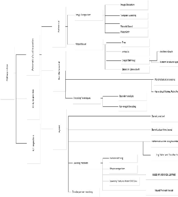
In this part we will summarize most of recent work on different PCB inspection approaches. Figure 1 explores the most common PCB inspection techniques into three categories reference comparison approach, design rule checking (non-referential) approach, and hybrid approach [6].
As described in introduction Referential techniques divided into two types Image comparison and Model based. For non- Referential has we recorded three types. Encoding Techniques include (Run-length, Boundary analysis), Morphological process based and Hierarchical Marked Point
IJSER © 2014 http://www.ijser.org
International Journal of Scientific & Engineering Research, Volume 5, Issue 7, July-2014 1097
ISSN 2229-5518
Process. Finally the Hybrid techniques, we summarize sum of their techniques (Generic, Genetic based, Learning methods, circular pattern matching, Log gabor filter and Classifier Fusion, Pattern detection using boundary analysis). Below we will describe techniques not included in Moganti96 Survey.
Fig. 1 classification of PCB inspection techniques.
Reference based techniques based on point or feature comparison between a reference image (golden image) and input image. It requires much time for image processing and enhancement; specially image registration task before image comparison applied.
Mauro and Roberto [38] introduced a technique for PCB inspection based on the comparison of the connected table (is a list of a list of connected PCB holes) of a Reference Image and a Test Image. The method is based on connected component analysis, which is a natural way to extract the connectivity information of the conductors of a PCB. The registration of the PCB holes, which is a common problem related to referential model techniques, is solved by the concept of zone of influence of each hole (zone of influence of a point is the region where all the points are nearer to that point than any other point in the image) and Labeling to extract the conductor connectivity of the PCB image. The implementation of this technique is using standard Morphology Image Processing techniques. This technique is impractical for manufacturing as it has long processing time
53sec (in Sun Sparc5 with 32 MB of memory) even with proposal of no (reading and writing files) and expected time about 5 sec. also many types of defects can't be covered (mouse bite, under etching, over etching, Variations between the printed lines).
Zuwairie and Syed [40] proposed an automated visual printed circuit board (PCB) inspection system based on a two-dimensional HAAR wavelet transform. During the inspection, two type of images are required; reference and tested PCB images. The wavelet transform is applied to the reference and tested PCB images. According to previously proposed wavelet-based PCB inspection algorithm, a reference comparison between the reference and tested PCB images has been done in wavelet domain by employing image difference operation. However, in practice, this operation also bring along the unwanted noise due to misalignment and uneven binarization. Thus, in this system, for the real-time implementation, the image difference operation between the reference and tested PCB images is replaced with image subtraction. The output of the image subtraction operation can be differentiated as positive, negative, and zero images. By doing so, a noise elimination procedure is applied to positive and negative images, resulting noise free positive and negative images. Lastly, the noise free images are subjected to XOR logic operation to generate the output of the inspection system. This system is well suited for small and medium scale PCB manufacturers where the sophisticated alignment facilities are hard to purchase.
Noor and Zuwairie [6] proposed an algorithm to group the defects found on bare PCB. Using a synthetically generated PCB image, the algorithm is able to group 14 commonly known PCB defects into five groups. The proposed algorithm includes several image processing operations such as image subtraction, image adding, logical XOR and NOT, and flood fill operator. The algorithm needs to be improved to achieve better result, which is to classify all the 14 types of defects separately. Also unwanted noise should be considered.
Fabiana and Flávio [7] present a Computer Vision system for printed circuit board (PCB) automated inspection in the proposed Computer Vision PCB Inspection System they considered the first manufacturing stage, i.e., the board printing in PCB manufacturing process. They first compared a PCB standard image with a PCB image, using a simple subtraction algorithm that can highlight the main problem- regions. Then they used connection analysis to find fatal and potential errors, like breaks and circuit shorts. In other to develop this methodology in real PCB, they propose to magnify the problem-regions and start to find the errors in a set of PCB sections, which are smaller than the main PCB image. This approach seems to be very effective if applied in a real time inspection system. Therefore, they propose a new algorithm to solve PCB inspection problem, considering its efficiency in reducing the computational time. It is fast algorithm but constraint only on PCB printed process while
IJSER © 2014 http://www.ijser.org
International Journal of Scientific & Engineering Research, Volume 5, Issue 7, July-2014 1098
ISSN 2229-5518
most of PCB defects happen in the subsequent processes. Also they confirm that the environment lighting should be uniform and that all inspected PCB belong to the same category. And will be necessary to calibrate the system every time we change the reference PCB or environment illumination.
Lin and Zhou[42] proposed an algorithm for PCB inspection based on Mathematical Morphology. In this work, the conception of linkage information table was presented which is regarded as correlation features of template PCBs. This work also includes pre-processing and feature extractor. Compared with features between detected images and template images based on linkage information table, those defects existed in tested PCBs can be identified, which has achieved the automatic identification and real time inspection. Proved by some experiments, this algorithm will largely compress feature data volume, decrease correlation workload and decrease data processing time. Through experiments, this algorithm can inspect ordinary defects fast and precisely. At last, this work has these following conclusions:
1) The noises are diminished in all images by using
median filtering method, which has following merits: small data number, short analyzing time, simple algorithm.
2) The defect inspecting method based on linkage information table of comparison with template and
tested images was presented, which need images not to be located at each other precisely, and largely decrease the required precision on hardware.
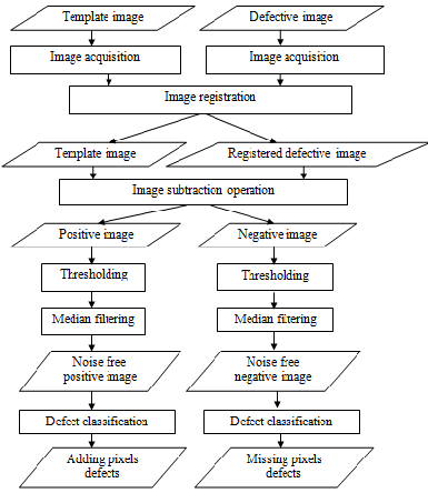
Ismail and Syed [16] proposed an algorithm for detecting six types of defects (pin hole, missing hole, short circuit, under- etch, open circuit and mouse-bite) on bare PCBs based on Image subtraction technique. Figure 2 represent the detection steps:
Fig. 2 Block diagram of the PCB inspection system
After images have been captured, image registration is executed to obtain a well-aligned defective image. Then, image subtraction operation, minimum thresholding and median filtering are used to get noise-free positive and negative images. Next, defect classification algorithms that have been taken from (Ismail and Zuwairie [43]) are employed to classify six printing defects as mentioned. The system was proven to be an alternative way to efficiently detect and classify defects. Furthermore, the system is cheap as mechanical alignment facility is no need to purchase.
The non-reference inspection methods do not need any reference image or pattern to work with. These methods are also called the design-rule inspection technique. The patterns and tracks of inspected image are checked with the design specification standards. Non-reference inspection methods can avoid the disadvantages of reference methods, but these methods may miss defects that do not violate the design rules.
In 1996, Borba and Facon proposed a non-reference
inspection method. It can detect defects without considering a reference board. The research succeeded in verifying vertically, horizontally and 45 degrees oriented traces.
Csaba [13] introduced a probabilistic approach for optical quality checking of solder pastes (SP) in Printed Circuit
IJSER © 2014 http://www.ijser.org
International Journal of Scientific & Engineering Research, Volume 5, Issue 7, July-2014 1099
ISSN 2229-5518
Boards (PCB) based on Hierarchical Marked Point Process (HMPP). Dealing with unregistered image inputs, it is required to address at the same time SP identification, and detection of special soldering errors, called scooping. Scooping occurs when the squeegee blade enters into the stencil aperture and removes paste from the center of the print. This is caused by high print pressure and can be exaggerated by rubber blades and large stencil apertures. A single scoop in a PCB does not cause a critical quality problem, however, if the number and summarized volume of such artifacts surpass a given threshold, the board should be withdrawn. For this reason he introduced a novel Hierarchical Marked Point Process (HMPP) framework, which is able to handle the paste and scooping extraction problems simultaneously, so that the SPs and included scoops have a parent–child relationship. A global optimization process attempts to find the optimal configuration of entities, considering the observed data, prior knowledge, and interactions between the neighboring circuit elements. The proposed method is evaluated on a real PCB image set containing more than 3000 SPs and 600 scooping artifacts. A morphology-based baseline method is also introduced for the problem and used as reference for qualitative and quantitative comparison against the proposed model. Experiments reported in this work confirmed the superiority of the proposed HMPP model and its usability for forthcoming industrial inspection systems over tested Morph system.
Hybrid inspection methods involve a combination both of reference and non-reference inspection methods. These methods have the advantages of these two techniques, but hybrid inspection methods are too complex to implement.
Chen and Zhang [39] presented a smart machine vision (SMV) system for printed circuit board (PCB) inspection. It consists of two modules, LIF (Learning Inspection Features) and OLI (On-Line Inspection). The LIF module automatically learns inspection features from the CAD files of a PCB board. The OLI module runs on-line to inspect PCB boards using a high-resolution 2-D sensor and the knowledge provided by the LIF components. Some example of learned features:
• Number of pads on each array,
• Location of each pad,
• Shape of each pad,
• Fill or no-fill status of each pad, and
• Location of every fiducial points on each PCB image.
The system has been tested over 8000 boards on a manufacturing line and the detection accuracy was above
97%.
Chin and Chun [8] present a Fourier descriptor based image alignment algorithm (FDBIA) for applications of automatic optical inspection (AOI) performed in real-time environment. It deliberates component detection and contour tracing algorithms and uses the magnitude and phase information of
Fourier descriptors to establish correspondences between the target objects detected in the reference and the inspected images. To enhance the computational efficiency, the proposed component detection and contour tracing algorithms use the run length encoding (RLE) and Blobs tables to represent the pixel information in the regions of interest. The Fourier descriptors derived from the component boundaries are used to match the target objects. Finally, the transformation parameters for aligning the inspected image with the reference image are estimated based on a novel phase-shifted technique. Experimental results show that the proposed FDBIA algorithm sustains similar accuracy as achieved by the commercial software Easyfind against various rotation and translation conditions. Also, the computational time consumed by the FDBIA algorithm is significantly shorter than that by Easyfind.
Wu and Chen [29] proposed an Image-array-based automatic optical inspection system captures multiple images of the inspected printed circuit board through synchronous exposure. Design error of the mechanism always leads to geometric errors in the image such as translation, rotation and scaling distortion. These errors make severe displacements in the image. To solve such problems, a concise and rapid error correction algorithm is proposed base on multiple point interpolation. Experiments show that the algorithm can assure rapid and correct mosaic of images of the whole printed circuit board.
Cai and Huang [30] proposed an effective framework for PCB Automatic Optical Inspection. First, a simple strategy that establishes accurate registrations between template image and inspecting images is proposed. Then they describe how to construct multi-layers PCB template based on cluster analysis which ensure that the color information is not lost. Finally they discuss the existence and classification of defects. Experimental results indicate that the registration speed and detection ability is greatly enhanced.
Chia-Te and Wen-Hao [32] researched for a new automated optical inspection system (AOI) to improve the inspection rate of defects, which has multi-color illuminator, and can capture images of the tested High Density Interconnection Printed Circuit Board (HDI PCB) by using machine vision, and also can identify several of defects quickly and accurately by a new-designed image processing software systems. The results of experiments prove that PCB defects inspection rate of the new AOI is improved and the false alarm rate of defects is reduced to 0.3%.
Syamsiah and Jonathan [5] presented a novel integrated system in which a number of image processing algorithm are embedded within a Genetic Algorithm (GA) based framework in order to provide an adaptation and better quality analysis with less computational complexity while maintaining flexibility to a broad range of defects. Their simulations on real PCB images demonstrate that the HGA is robust enough to detect any missing components and cut solder joint with any size and shape with significant
IJSER © 2014 http://www.ijser.org
International Journal of Scientific & Engineering Research, Volume 5, Issue 7, July-2014 1100
ISSN 2229-5518
reduction in computational time compared to conventional approaches. While it use a tailored hybrid GA (HGA) is used to estimate geometric transformation and needs classification process to recognize the type of defect for decision making by the system itself or human operator.
Crispin and Rankov [41] investigate methodologies for locating and identifying multiple objects in images used for surface mount device inspection. Their work focuses on automated object-recognition techniques for locating multiple objects using grey-model fitting for producing a generalized template for a set of components. The work uses the normalized cross correlation (NCC) template-matching approach and examines a method for constraining the search space to reduce computational calculations. The search for template positions has been performed exhaustively and by using a genetic algorithm.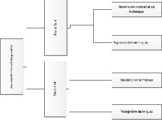
Wu Hao, Zhang Xianmin [4] proposed a neural network combined with genetic algorithm for the diagnosis of solder joint defects on printed circuit boards (PCBs) assembled in surface mounting technology (SMT). Six types of solder joint have been classified in respect to the reality in the manufacture. The images of solder joint under test are acquired and 14 features are extracted as input features for the classification. The neural network is easily become over- fitting because these input features are not independent of each other, so the genetic algorithm is introduced to select and remove redundant input features. The experimental results have proved that the neural network combined with genetic algorithm reduced the number of input feature and had a satisfying recognition rate. While it has a significant time for classification as a requirement for manufacturing.
Fig. 3 Classification of PCB inspection techniques. Figure 3 represents another view of visual inspection
techniques based on [36]; Front-End and Back-End. Front-
End examines techniques for image enhancement and
segmentation; that is those techniques related to detection
phase only. While Back-End includes the next step in visual inspection process; classification and Recognition phase.
S.Yarlagadda and C.Fookes [36] proposed two inspection modules for an automatic solder joint classification system. The ‘‘front-end’’ inspection system includes illumination normalization, localization and segmentation. The ‘‘back- end’’ inspection involves the classification of solder joints using the Log-Gabor filter and classifier fusion. Five different levels of solder quality with respect to the amount of solder paste have been defined. The Log-Gabor filter has been demonstrated to achieve high recognition rates and is resistant to misalignment. This proposed system does not need any special illumination system, and the images are acquired by an ordinary digital camera. This system could contribute to the development of automated non-contact, non-destructive and low cost solder joint quality inspection systems. Experimental results demonstrate that the proposed system improves performance and robustness in terms of classification rates. However, further improvements can be expected from the current technologies. More robust features could be developed by focusing on the errors of the current algorithm and the use of multiple views of solder joints could also improve classification performance.
As the rapid technology improvement of electronic industry and heavy mass production the need for AOI system arise as a need of quality and speed. In this survey we tried to cover most recent researches and algorithms in AOI system.
• A remarkable work appeared regarding of detection Bare PCB and less for PCB with SMT components defects detection. But still there are some issues regarding speed and false alarms.
• A few recent researches introduced regarding non- referential techniques.
• Most of the techniques require special environment conditions.
• A little research introduced regarding defects classification.
[1] Lee ZS, Lo RC (2002) “Application of vision image cooperated with multi-light sources to recognition of solder joints of PCB”, The
2002 Conference on Technologies and Applications of Artificial
Intelligence (TAAI 2002). pp. 425–430.
[2] Yang FC, Kuo CH, Wing JJ, Yang CK (2004) “Reconstructing the 3D solder paste surface model using image processing and artificial neural network”, IEEE international conference on Systems, Man and Cybernetics (10-13 Oct. 2004) ,The Hague, The Netherlands; Vol 3: pp. 3051-3056.
IJSER © 2014 http://www.ijser.org
International Journal of Scientific & Engineering Research, Volume 5, Issue 7, July-2014 1101
ISSN 2229-5518
[3] Lin SC, ChouCH, Su CH (2007) “A development of visual inspection system for surface mounted devices on printed circuit board” Industrial Electronics Society, 2007. IECON 2007. 33rd Annual Conference of the IEEE; Taipei Taiwan ; pp. 2440–2445.
[4] Wu Hao,Zhang Xianmin, Kuang Yongcong, Ouyang Gaofei, Xie Hongwei (2013) “Solder joint inspection based on neural network combined with genetic algorithm” Elsevier, International Journal for Light and Electron Optic 2013; Vol 124, Issue 20, October 2013, pp. 4110–4116.
[5] Syamsiah Mashohor, Jonathan R. Evans and Ahmet T. Erdogan (2006) “Automatic Hybrid Genetic Algorithm Based Printed Circuit Board Inspection”, IEEE, 2006. AHS 2006. First NASA/ESA Conference on Adaptive Hardware and Systems (AHS'06 Istanbul) 15-18 June 2006, pp. 390-400.
[6] Noor Khalid, Zuwairie Ibrahim, And Mohamad Abidin (2008) “An Algorithm to Group Defects on Printed Circuit Board for Automated Visual Inspection”. International Journal of Simulation Systems, Science & Technology IJSSST, Vol.9, No.2, May 2008 pp. 1-10.
[7] Fabiana R. Leta, Flávio F. Feliciano, Flavius P. R. Martins (2008) “Computer Vision System for Printed Circuit Board Inspection” ABCM Symposium Series in Mechatronics - Vol. 3: pp. 623-632.
[8] Chin-Sheng Chen a, Chun-Wei Yeh a, Peng-Yeng Yin (2009) “A novel Fourier Descriptor Based Image Alignment Algorithm for Automatic Optical Inspection” Elsevier Journal of Visual Communication and Image Representation Vol 20, Issue 3, April
2009, pp. 178–189.
[9] Chern-Sheng Lin, Su-ChiChang, Yun-LongLay, Mau-ShiunYeh, Chi-ChinLin (2010) “A novel Positioning Method for Optical Automatic Inspection of An LCD Assembly Process” Elsevier International Journal for Light and Electron Optic (2010) Vol 121, Issue 12, June 2010, pp. 1089–1095.
[10] Der-Baau Perng · Yen-Chung Chen (2010) “An advanced Auto- inspection System for Micro-router Collapse” Springer Journal of Machine Vision and Applications Vol 21 Issue 6, October 2010 pp.
811-824.
[11] Guifang Duan · Yen-Wei Chen · Takeshi Sukegawa (2010) “Automatic optical flank wear measurement of microdrills using level set for cutting plane segmentation” Springer Machine Vision and Applications August 2010 , Vol 21 Issue 5: pp. 667–676.
[12] N.S.S. Mar, P.K.D.V.Yarlagadda, C.Fookes (2011) “Design and development of automatic visual inspection system for PCB manufacturing” Elsevier Robotics and Computer-Integrated Manufacturing Vol 27, Issue 5, October 2011, pp. 949–962.
[13] Csaba Benedek (2011) “Detection of soldering defects in Printed Circuit Boards with Hierarchical Marked Point Processes” Elsevier Pattern Recognition Letters Vol 32, Issue 13, 1 October
2011, pp. 1535–1543.
[14] Rong-Fong Fung, Chih-Yu Yang, Ching-Tsung Lai (2011) “
Graphic supervisory control of an automatic optical inspection for
LED properties” Elsevier Measurement Vol 44, Issue 8, October
2011, pp. 1349–1360.
[15] Du-Ming Tsai, Hsin-Yang Tsai (2011) “Low-contrast surface inspection of mura defects in liquid crystal displays using optical
flow-based motion analysis” Springer Journal Machine Vision and Applications Vol 22 Issue 4, July 2011pp. 629-649.
[16] Ismail Ibrahim, Syed Abdul Rahman, Syed Abu Bakar, Musa Mohd Mokji, Jameel Abdulla Ahmed Mukred, Zulkifli md Yusof, Zuwairie Ibrahim, Kamal Khalil, Mohd Saberi Mohamad (2012) “A printed Circuit Board Inspection System with Defect Classification Capability” International Journal of Innovative Management, Information & Production ISME International March 2012, Vol 3, No 1: pp.82-87.
[17] Sharat Chandra Bhardwaj (2012) “Machine Vision algorithm for PCB Parameters Inspection” National Conference on Future Aspects of Artificial intelligence in Industrial Automation (NCFAAIIA 2012), Proceedings published by International Journal of Computer Applications® (IJCA),No 2, pp. 20-24
[18] Chern-Sheng Lin, Guo-Hao Loh, Chuen-Lin Tien, Tsung-Chih Lin, Yih-Chih Chiou (2013) “Automatic optical inspection system for the micro-lens of optical connector with fuzzy ratio analysis” Elsevier International Journal for Light and Electron Optic 2013
Vol 124, Issue 17, September 2013, pp. 3085–3090
[19] Chuan-Yu Chang, Senior Member, IEEE, Chun-Hsi Li, Student Member, IEEE, Si-Yan Lin, and MuDer Jeng, Fellow, IEEE (2009) “Application of Two Hopfield Neural Networks for Automatic Four-Element LED Inspection” IEEE Transactions on Systems, Man, And Cybernetics—Part C: Applications And Reviews, Vol
39, No 3, pp. 352-365, May 2009.
[20] Su-Hwan Kim a, Jee-Hyun Kim b, Shin-Won Kang (2011) “Nondestructive defect inspection for LCDs using optical coherence tomography” Elsevier Displays Vol, Issue 5, December
2011, pp. 325–329.
[21] C.W. Liao, Y.S. Tarng (2009) “On-line automatic optical inspection system for coarse particle size distribution” Elsevier Powder Technology Vol 189, Issue 3, 13 February 2009, pp. 508-513
[22] Toshifumi Honda, Hisae Yamamura, Syouji Ueda,Minoru Kawabata and Takanori Ninomiya (1994) “Automated Visual Inspection System for Electronic Devices Mounted on Printed Circuit Boards Using Light-Section Method”, MVA'94 IAPR Workshop on Machine Vision Applications Dec. 13-15, 1994
Kawasaki Japan. pp. 575-578
[23] Moganti, M., Ercal, F., Dagli, C. H. and Shou, Tsunekawa (1996) “Automatic PCB Inspection Algorithms: A Survey”, Computer Vision and Image Understanding, Vol. 63, No.2, pp. 287 – 313.
[24] Yung-Nien Sun, and Ching Tsorng Tsai (1992) “A New Model- Based Approach for Industrial Visual Inspection”, Elsevier Journal of Pattern Recognition, Vol 25, Issue 11, November 1992, pp. 1327–1336.
[25] Ji-joong Hong, Kyung-ja Park and Kyung-gu Kim (1998) “Parallel processing machine vision system for bare PCB inspection”, Industrial Electronics Society, IECON ’98. Proceedings of the 24th Annual Conference of the IEEE Aachen Germany Vol 3, pp. 1346
– 1350.
[26] Lin, Chern-Sheng, Ho, Chen-Wei,Yang, Shih-Wei,Chen, Der-Chin, Yeh, Mau-Shiun (2010) “Automatic optical inspection system for the image quality of micro lens array”, Indian Journal of Pure & Applied Physics. Vol 48, September 2010, pp. 635 – 643.
IJSER © 2014 http://www.ijser.org
International Journal of Scientific & Engineering Research, Volume 5, Issue 7, July-2014 1102
ISSN 2229-5518
[27] Bin Ren , Lianglun Cheng (2009) “SMT Automatic Optical Inspection Path Planning Based on MDSPSO Algorithm”, International Conference on Computational Intelligence and Natural Computing 2009 Wuhan China Vol 2: pp. 134-137
[28] Yen-Chung Chen, Jiun-Hung Yu, Mu-ChiauXie and Fang-Jung Shiou (2011) “Automated optical inspection system for analogical resistance type touch panel”, International Journal of the Physical Sciences Vol. 6(22), pp. 5141-5152, 2 October, 2011.
[29] Jianjie Wu, Zhongbing Chen (2011) “A Concise and Rapid Error Correction Algorithm in Automatic Optical Inspection of Solder Paste”, IEEE Proceeding ICICIS '11 Proceedings of the 2011
International Conference on Internet Computing and Information
Services Hong Kong, Vol 1: pp. 325-329.
[30] Yu Cai, Yanjin Huang, Shugong Zhang (2012) “Research of Defect Inspection and Processing in PCB Automatic Optical Inspection”, Proceeding ICECC '12 Proceedings of the 2012 International Conference on Electronics, Communications and Control, Zhoushan China pp. 803-806.
[31] Guangjie Xiong, Jingjing Lu, Siyuan Wu (2012) “New Automatic
Optical Inspection System for PCB”, Proceeding ICECC '12
Proceedings of the 2012 International Conference on Electronics,
Communications and Control, Zhoushan China pp.1270-1273.
[32] Chia-Te Liao, Wen-Hao Lee, Shang-Hong Lai (2012) “A Flexible PCB Inspection System Based on Statistical Learning”, Journal of Signal Processing Systems Vol 67 Issue 3, June 2012, pp. 279-290.
[33] Mika Liukkonen, Elina Havia, Yrjö Hiltunen (2012) “Review: Computational intelligence in mass soldering of electronics - A survey”, Journal Expert Systems with Applications: An International Journal Vol 39 Issue 10, August, 2012, pp. 9928-9937.
[34] R. C. Gonzalez and Richard E. Woods (1993) “Digital image processing” Book, Addison-Wesley Publishing Company Inc, ISBN 0-201-50803-6.
[35] Ajay Pal Singh Chauhan, Sharat Chandra Bhardwaj (2011) “Detection of Bare PCB Defects by Image Subtraction Method using Machine Vision”, Proceedings of the World Congress on Engineering 2011 Vol II pp1597-1601, WCE 2011, July 6 - 8, 2011, London, U.K.
[36] N.S.S. Mar, C. Fookes, P.K.D.V. Yarlagadda (2009) “Design of automatic vision-based inspection system for solder joint segmentation”, Journal of Achievements in Materials and Manufacturing Engineering, Vol 34 Issue 2, June 2009, pp. 145-
151.
[37] Hong Kyu Chung,Rae-Hong Park (1997) “Two-stage high- precision visual inspection of surface mount devices”, Journal of Electronic Imaging Vol 6(4), pp. 517–524 (October 1997).
[38] MAURO HIROMU TATIBANA, ROBERTO DE ALENCAR LOTUFO (1997) “Novel Automatic PCB Inspection Technique Based on Connectivity” IEEE, X Brazilian Symposium on Computer Graphics and Image Processing, Campos do Jordao Brazil, 14-17 Oct 1997, pp. 187 – 194
[39] Tie Qi Chen, JianXin Zhang, YouNing Zhou and Yi Lu Murphey (2001) “A Smart Machine Vision System for PCB Inspection”, 14th International Conference on Industrial and Engineering Applications of Artificial Intelligence and Expert Systems,
IEA/AIE 2001 Budapest, Hungary, June 4–7, 2001 Proceedings, Vol 2070, pp. 513-518.
[40] Zuwairie Ibrahim , Syed Abdul Rahman Al-Attas (2004) “Wavelet-Based Printed Circuit Board Inspection System”, International Journal of Signal Processing Vol 1 No 2, pp. 73-79.
[41] A. J. Crispin & V. Rankov (2007) “Automated inspection of PCB components using a genetic algorithm template-matching approach”, Springer International Journal of Advanced Manufacturing Technology (2007) Vol 35: pp. 293-300.
[42] Li-zong Lin, Luo-shan Zhou, Jian-ding Wan and Zhi-qin Qian (2009) “Study of PCB Automatic Optical Inspection System Based on Mathematical Morphology”, IEEE International Conference on Computer Technology and Development 2009, Kota Kinabalu Malaysia, Vol 2:pp. 405-408.
[43] Ismail Ibrahim, Zuwairie Ibrahim, Kamal Khalil, Musa Mohd Mokji, Syed Abdul Rahman Syed Abu Bakar, Norrima Mokhtar and Wan Khairunizam Wan Ahmad (2012) “An Improved Defect Classification Algorithm For Six Printing Defects And Its Implementation On Real Printed Circuit Board Images” International Journal of Innovative Computing, Information and Control Vol 8, No 5(A), pp. 3239-3250, May 2012.
IJSER © 2014 http://www.ijser.org