International Journal of Scientific & Engineering Research, Volume 4, Issue 12, December-2013 1393
ISSN 2229-5518
Analyzing 3D IC PDNs Using Multiple Clock Domains to Obtain Worst-Case Power Supply Noise and Temperature Variations
Abstract— This work presents power and thermal integrity issues obtained from multiple clock domains in 3D IC Power Delivery Network [PDN]. First, we introduce how power supply noise is distributed on each tier and how it derives to worst case noise. Second, we examine the performance of thermal analysis in each tier. Finally, we present how heat is distributed among multiple clock domains. Experiment results show that the amount of noise and heat transfer in each tier is mainly contributed from TSVs. SPICE simulation is used to obtain the worst- case power supply noise and temperature Variations on 3D IC PDNs.
KEY WORDS: 3DIC, PDNs, TSVs, C4s, PCB, Voltage Drop, SOC, NOC.
. —————————— ——————————
Three-dimensional (3D) integration emerges as a promising solution to the many limitations of modern integrated circuits. The salient characteristics of this novel technology include the significant reduction in the interconnect length
and the inherent capability to integrate heterogeneous
In 2D SoCs, choked by interconnect limitations, networks- on-chip (NoCs) was developed [1], composed of switches and links, have been proposed as a scalable solution to the global communication challenges. Compared to previous architectures for on-chip communication, such as bus-based
and point-to-point networks, Network-on-Chips (NoCs)
IJSER
technologies. To exploit, however, these advantages specific
manufacturing and design issues need to be resolved. In these 3D ICs multiple tiers are stacked above each other and vertically interconnected using through-silicon vias (TSVs) are emerging as a promising technology for System- on-Chips (SoCs). As compared to 2D designs, 3D circuits permit reduced latencies for critical interconnect structures, resulting in higher system throughput, performance, and power, and allowing other benefits, such as heterogeneous integration. All of these flexibilities enable the design of new, high-performance SoC structures that were previously thought to have prohibitive overheads. In spite of well- known challenges, such as thermal bottlenecks (to which several solutions have been proposed), the benefits of 3D integration are considerable. In the context of intra chip communication, 3D technologies have created significant opportunities and challenges in the design of low-latency, low-power, and high-bandwidth interconnection networks.
————————————————
• Research Scholar, Dayananda Sagar College of Engg. VTU, Karnataka, India , PH- 9986438788. E- mail:sinchu22@yahoo.co.in1
have been shown to provide better predictability, lower
power consumption, and greater scalability. 3D circuits
enable the design of more complex and more highly
interconnected systems. In this context, NoCs promise major benefits but impose new constraints and limitations. Compared to wire interconnects; NoCs not only enable scalable and parallel communication within and across 3D tiers but also reduce the number of TSVs for vertical interconnects. However, 3D NoC design introduces new issues, such as the technology constraints on the number of TSVs that can be supported, problems related to optimally determining tier assignments, and the placement of switches in 3D circuits, and accurate power and delay modeling issues for 3D interconnects. A microelectronic power distribution network (PDN) is a system which supplies power to integrated circuits. A PDN consists of interconnect wires with decoupling capacitors (decap) on a printed circuit board (PCB), an integrated circuit package, and a circuit die. PDN has been a popular research topic for decades. Most of the research works fall into the following categories: simulation, analysis, and optimization. With the emerging 3D IC technology recently, more and more research efforts have been made on 3D PDNs as well. The use of multiple clock domains provides a challenge on reliable delivery of power supply voltage to each tier on a
3D stack. For 2D ICs, power delivery networks are mainly structured as regular meshes with metal tracks running in perpendicular to each other. Other works, have explored the non-regularity of power meshes for reducing voltage
IJSER © 2013 http://www.ijser.org
International Journal of Scientific & Engineering Research, Volume 4, Issue 12, December-2013 1394
ISSN 2229-5518
drop. Regardless of their structure, power delivery networks are designed to deliver voltage reliably such that
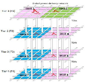
the underlying circuits can function properly. Any deviation from the supply voltage can obtain optimal performance of devices and consequently leading to circuit delay and throughput reduction. Several papers can be found in literature that looks into 3D power delivery networks. Authors in [2] provide models to analyze 3D PDNs. Works on [3-9] investigate different TSV technologies, floor planning and decoupling capacitance insertion for power grid optimization. There are various challenges that multiple clock domains introduce to 3D PDNs. Assume that there are two clock domains on tier 1 (T1 ) as shown in Fig 1. Block 1 with freq1 has fast switching and power hungry circuits, while block 2 with
transfer from T3 to T4 . Worst-case noise may occur when a block is experiencing self-induced noise and transferred
noise from neighboring clock domains or tiers that can lead to critical performance issues. Heat dissipation and transfer among tiers exhibits a similar trend.
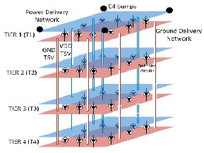
In this work, we investigate power supply noise and temperature distribution on a four-tier power delivery network with various clock domains. An illustration is shown in Fig 2. The analyses are based on the RLC model representation of the power grid, package, and switching circuits. We utilize existing physical models for studying power supply noise on 3D power grids and further enhance them to include the thermal effects.
IJSER
Fig 2. Illustration of power and ground delivery networks for a three-
tier system.
Clermidy.F et al. investigated three promising perspectives for short to medium terms adoption of such technology in high-end System-on-Chip built around multi-core
Fig 1. Illustration of four-tier 3D PDN with several blocks representing multiple clock domains.
freq2 has slow switching with low power demand circuits.
Both these blocks operate with the same voltage supply and share the global power grid. Due to fast and frequent switching of block 1, voltage fluctuations (power supply noise) are introduced on the power grid, which consequently impact the performance of block 2. Furthermore, TSVs serve to connect power networks among tiers but undesirably they also transfer power supply noise between them. For example, block 3 in tiers 2 (T2 ) will also experience excessive voltage fluctuations due to the noise transfer from T1 to T2 , similarly block 5 in tiers
3 (T3 ) also experience excessive voltage fluctuations due to
the noise transfer from T2 to T3 and block 7 in tiers 4 (T 4 )
experience excessive voltage fluctuations due to the noise
architectures, the wide bus concept will help solving high bandwidth requirements with external memory [1]. Huang.G et al. proposed an analytical physical model which is derived to incorporate the impact of 3D- integration on power supply noise in which the model has less than 4% error compared to SPICE simulations [2]. Pak.J.S et al. introduced the impedance of a power- distribution network (PDN) in three-dimensionally stacked chips with multiple through-silicon-via (TSV) connections (a 3D TSV IC) which were modeled and analyzed using a power/ground (P/G) TSV array model based on separated P/G TSV and chip-PDN models at frequencies up to 20 GHz [3]. Healy.M.B et al. presented the design of many-tier (more than 4 tiers stacked) 3D power-supply networks and demonstrates a technique specific to 3D systems that improves IR-drop over a straightforward extension of traditional design techniques [4]. Khan.N.H et al. analyzed
IJSER © 2013 http://www.ijser.org
International Journal of Scientific & Engineering Research, Volume 4, Issue 12, December-2013 1395
ISSN 2229-5518
the impact of through-silicon via (TSV) size and spacing, of controlled collapse chip connection (C4) spacing, and of
dedicated power delivery TSVs. In addition to considering typical cylindrical or square metal-filled TSVs (core TSVs), they also investigate using coaxial TSVs for power delivery resulting in reduced routing blockages and added coupling capacitance [5]. Wright.S, et al. introduced package model in which controlled collapse chip connection (C4) bumps are used for the package, which are an industry standard for flip-chip technology [10]. The bumps sizes are of 100um width and 200um pitch and its RL parasitic are extracted as
10mΩ and 60pH [10]. They assumed an array of C4 bumps
where half are used for supplying power (VDD) and ground (GND), respectively. The contact resistance and reliability test results to date suggest that reliable, high- current, high-density bump interconnections can be achieved for Si-carrier technology. Fuchs.C, et al, presented a TSV model in which they studied high-density TSVs with dimensions as 15μm length, 3μm diameter, and 60μm pitch. RLC parasitics of TSV have been extracted as Rtsv=100mΩ, Ltsv=10pH, and Ctsv=40fF [11]. We assume that TSVs are inserted in an array and uniformly
Jain.A, et al. presented a thermal model in which simultaneous switching circuits on a tier and neighboring
tiers can lead to non-uniform power and heat distributions. Impedance of power and ground networks may vary due to non-uniform thermal distribution, as resistivity is a function of temperature. Thus, at nodes with high temperature, voltage droop worsens. Also, large amount of currents flowing through power and ground networks elevate temperature even more, which over long periods of time can cause Joule heating and/or electro migration. Hence, voltage droop and thermal distributions are interdependent and we consider them simultaneously [8] [12].
Then we perform continuous electrical and thermal analyses to determine voltage droop and temperature distribution on each tier. To do this, a thermal model of the four-tier system is built, where the principle of electrical- thermal duality is obtained. Duality is based on equivalence of electrical current through an electrical resistor to heat flow through a thermal resistor and voltage difference
equivalence to temperature difference. Thermal resistance
IJSER
distributed. Similarly, we assume that half of TSVs are for
power and ground, respectively. Pak.J.S, et al. obtained
RLC models for 3D PDNs, which consists of regular mesh networks for each tier that is connected together using TSVs. They assumed power grids are uniform, which means that each power track has a uniform width throughout its length, whereas the width of each track can vary as illustrated in Figures 1 and 2. RLC parasitics, Rgrid , Lgrid , and Cgrid of each power track can be extracted based on its dimension. In this study, we consider power tracks of
1000μm length and 10μm to 30μm widths. In this study, we also consider decoupling capacitance (decaps) based on intentionally inserted and non-switching circuit decaps [3]. Todri.A, et al. proposed a switching circuit model in which each working core or functional block can represent circuits of different functionalities, power demands and operating frequencies. From the power grid analysis perspective, these switching circuits draw current from the power grid and are commonly modeled as switching current sources with specific parameters to represent the characteristics of the underlying circuits. Switching circuits are commonly modeled as triangular current sources to represent peak and leakage current and peak, rise and fall times as I peak, I leak, tpeak , trise , and t fall. To represent the multiple clock domains, the operating frequencies of the functional blocks are varied such as to represent various switching clock frequencies. Time period of a switching clock for a block i, can be represented as tperiod (i) = 2(trise (i) + tfall (i) ) and clock frequency as freq (i) = 1/ t period (i ) [2-8].
models obtained from [8] [12] are applied to represent
PDNs, TSVs, and C4s. Heat is generated by Switching
circuits and are modeled as current sources to represent their power consumption. Temperature at heat sink is assumed 27°C. Thermal analysis is based on 1-D static analysis, and combined with electrical analysis, we re- compute voltage droop on each tier. Due to lack of space, details on thermal models can be found in [8].
To obtain multiple clock domain power grid analysis, we first describe how power grid node voltages are mathematically computed applying modified nodal analysis (MNA).
To apply the node voltage method to a circuit with n nodes
(with m voltage sources), perform the following steps:
• Selective a reference node (usually ground).
• Name the remaining n-1 nodes and label a current
through each passive element and each current
source.
• Apply Kirchhoff’s current law to each node not
connected to a voltage source.
• Solve the system of n-1-m unknown voltages.
The difficulty with this method comes from having to consider the effect of voltage sources. Either a separate
IJSER © 2013 http://www.ijser.org
International Journal of Scientific & Engineering Research, Volume 4, Issue 12, December-2013 1396
ISSN 2229-5518
equation is written for each source, or the super node method must be used. The rules for modified nodal analysis are mentioned below.
To apply the node voltage method to a circuit with n nodes
(with m voltage sources), perform the following steps:
• Selective a reference node (usually ground) and
name the remaining n-1 nodes. Also label currents
through each current source.
• Assign a name to the current through each voltage
source. We will use the convention that the current flow from the positive node to the negative node of the source.
• Apply Kirchhoff’s current law to each node. We will take currents out of the node to be positive.
• Write an equation for the voltage each voltage source.
• Solve the system of n-1 unknowns.
MNA applied to a circuit with only passive elements
o is an (n+m)x1 vector that holds only known quantities
o The top n elements are either zero or the sum and difference of independent current sources in the circuit.
o The bottom m elements represent the m
independent voltage sources in the circuit.
The circuit is solved by a simple matrix manipulation:
X= A-1 Z (2) Current flow on power grid branches and node voltages on power grid intersections respect the Kirchhoff’s current and voltage rules i.e. KCL and KVL. Thus, the equations of each node voltage can be obtained in matrices as:
V = AU = G-1 U (3) where G is the modified conductance matrix of the power grid, U is the vector of current sources, and V is the vector of node\ voltages. A node voltage, vi can be expressed as:
(resistors) and independent current and voltage sources
vi = ∑𝑛
𝑎𝑖𝑗. 𝑔𝑖𝑗𝑉𝑑𝑑 − 𝑛
results in a matrix equation of the form:
𝑗=1 ∑𝑘=1 𝑎𝑖𝑘. 𝐼𝑘
(4)
IJSER
AX = Z (1)
For a circuit with n nodes and m independent voltage
sources:
The A matrix:
• Is (n+m)x(n+m) in size, and consists only of known quantities.
• The nxn part of the matrix in the upper left:
o Has an only passive element.
o Elements connected to ground appear
only on the diagonal.
o Elements not connected to ground are both on the diagonal and off-diagonal
terms.
• The rest of the A matrix (not included in the nxn
upper left part) contains only 1, -1 and 0 (other values are possible if there are dependent current and voltage sources, we have not considered these
where n is the number of voltage nodes on the PDN, gij VDD is the conductance term, Ik is the current source at node k, and aij and aik are elements of matrix A.
Note that node voltage vi represents both power and ground node voltages. Solving for node equations (Eq 4) would rely on computing inverse matrix, which can be computationally expensive. There are several efficient and accurate linear algebra based methods for MNA analysis [2-
8]. Discussion of MNA solvers is not the scope of the paper
and perusal on these methods is left to the reader. Based on
the node voltages, one can easily compute the final node voltage using the superposition principle. The superposition applies to linear networks where the response of each frequency is combined together as:
Vi = Vi freq(1) + Vi freq(2) +.…+ Vi freq(m) +V0
cases.
• The x matrix:
𝑚
𝑟=1
𝑉𝑖 𝑓𝑟𝑒𝑞(𝑟) + 𝑉0 (5)
o Is an (n+m) x1 vector that holds the unknown quantities (node voltages and the currents through the independent voltage sources).
o The top n elements are the n node voltages.
o The bottom m elements represent the
where Vi freq(m) is the node voltage for each frequency domain, m is the number of different clock frequency domains, and V0 is the initial conditions node voltage. Based on the node voltages for each frequency, the amount of power supply noise can be derived by computing the voltage drop during a given time period as:
currents through the m independent voltage sources in the circuit.
• The z matrix:
PSNi freq (j) = ∫𝑡𝑠 (𝑉𝐷𝐷 − 𝑉𝑖 𝑓𝑟𝑒𝑞𝑗)𝑑𝑡
(6)
IJSER © 2013 http://www.ijser.org
International Journal of Scientific & Engineering Research, Volume 4, Issue 12, December-2013 1397
ISSN 2229-5518
where ts and te are starting and end time for computing the amount of voltage droop. Similarly, the total amount of power supply noise induced from different clock domains can be computed as:
Several setups were made with multiple clock domains to perform the experiments. In the experiments, we assume each tier has two cores (cores 1 and cores 2) that share the same power grid on a tier and there are a total of four tiers.
PSNi = ∑𝑚
PSN𝑖 𝑓𝑟𝑒𝑞𝑗 + PSNi0 (7)
Tier one is the closest to the package bumps, whereas tier four is next to heat sink and benefits from immediate
where PSNi0 is the initial condition power supply noise. Here, we also introduce the notion of self and transferred noise. Self noise is the amount of noise that a block i with clock frequency, freq k introduces on itself as PSNi self= PSNi freq(k) + PSNi0. Transferred noise is the amount of noise that block i experiences from other blocks with different clock frequencies (different from freqk) as PSNitransferred
cooling. From a wide range of operating frequencies, we
select three frequencies to represent low (L), mid (M) and high (H) clock frequencies. We apply various clock frequencies and investigate the voltage droop and temperature on the 3D PDN. We perform the followings and there results are listed in Table 1.
𝑚
𝑟=1,𝑟≠𝑘
PSN𝑖 𝑓𝑟𝑒𝑞 (𝑟). Similarly, temperature distribution
on 3D PDNs can be computed by applying superposition
principle. There are several works that discuss in-depth PDN thermal modeling [8] [12]. In this work, we utilize these models to perform simultaneous electrical and thermal analysis of 3D PDNs. By exploiting the principle of electro thermal duality, 3D PDN thermal networks can be
devised as electrical networks and solved accurately for
For this study, we apply the same clock frequency to all the
tiers and their cores. We study three setups (i.e. s1, s2, s3) as shown in second columns of Table 1. In setup s1, all the cores and tiers operate with low frequency clock domain, in setup s2 in mid clock frequency and setup s3 in high clock frequency, as shown in columns five to eight in Table 1. For each setup, we compute the worst-case power supply noise
IJSER
node temperatures similarly as node voltages. Based on 1-D
treatment of temperature distribution, temperature on PDN
segments can be derived as:
T = Gth -1. Qth = Hth Qth (8)
where Gth -1 is the thermal impedance matrix and Qth is the heat sources vector based on derived power consumption from electrical network. Node temperature can be expressed as:
(voltage drop in power and ground tracks) and
temperature on each tier as listed in columns 9 through 14.
We note that in general the worst voltage droop is measured on Tier 4 (furthest from package) and worst temperature is measured on Tier 2 or Tier 3 (middle of stack). We also note that high frequency clock domain (s3) introduces the most voltage droop and temperature rise. This is due to increased inductive parasitic impedance (jwL) with frequency increase and reduced effectiveness of
𝑛
𝑗=1
ℎ𝑡ℎ (𝑖)𝑗 𝑞𝑡ℎ(𝑗)
(9)
decoupling capacitances, as they cannot be recharged in
time before the next transition. Tier 2 or Tier 3 located in the
Overall, node temperature due to multiple clock domains can expressed as:
middle of the stack suffers from heat dissipation from both top and bottom tiers, hence it experiences the highest temperature.
𝑚
𝑗=1
𝑇𝑖 𝑓𝑟𝑒𝑞(𝑗) + 𝑇𝑖 (0)
(10)
where Ti 0 is initial temperature. Accuracy of the mathematical formulations for power supply noise and temperature are compared to HSPICE simulations. Results show the accuracy of the proposed method for deriving power supply and temperature distribution on 3D PDNs with multiple clocks domains. Moreover, experiments indicate that excessive noise and temperatures can be induced due to various clock frequencies. Furthermore, such analyses motivate deeper investigations into optimal design of 3D PDNs with multiple clock domains.
To highlight the impact of multiple clock domains, we investigate three setups s4, s5 and s6. For the simplicity, we choose these three cases, however more cases can be envisioned. We note that different assignment of clock domains on tiers and cores result into different voltage droop and temperatures. The worst voltage droop and temperature are measured on setup, s6 where there is up to
8mV and 10ºC difference from setup, s4. Such result shows
IJSER © 2013 http://www.ijser.org
International Journal of Scientific & Engineering Research, Volume 4, Issue 12, December-2013 1398
ISSN 2229-5518
TABLE 1. Worst-case power supply noise and temperature measurements on a three-tier PDN with multiple clock domains.
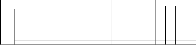
Setup Tier 1 Tier 2 Tier 3 Tier 4 Voltage Droop (mV) Temperature(0C)
One s1 clock s2 domain s3 | Core1 | Core2 | Core1 | Core2 | Core1 | Core2 | Core1 | Core2 | Tier1 | Tier2 | Tier3 | Tier4 | Tier1 | Tier2 | Tier3 | Tier4 | |
One s1 clock s2 domain s3 | L* | L | L | L | L | L | L | L | 73.4 | 92.3 | 94.6 | 97.6 | 72.5 | 74.6 | 35.2 | 28.6 | |
One s1 clock s2 domain s3 | M* | M | M | M | M | M | M | M | 74.6 | 96.5 | 98.2 | 102 | 72.7 | 75.2 | 35.6 | 28.9 | |
One s1 clock s2 domain s3 | H* | H | H | H | H | H | H | H | 76.2 | 104 | 105 | 112 | 75.4 | 78.5 | 34.2 | 30.1 | |
Two | s4 | M | H | M | H | M | H | M | H | 61.5 | 82.7 | 96.3 | 98.5 | 65.2 | 69.5 | 33.5 | 29.8 |
clock | s5 | L | M | L | M | L | M | L | M | 59.0 | 75.8 | 82.4 | 86.3 | 61.3 | 63.4 | 32.1 | 30.5 |
domain | s6 | H | L | H | L | H | L | H | L | 68.3 | 92.9 | 102 | 105 | 70.8 | 72.1 | 32.8 | 31.4 |
Three | s7 | M | H | L | M | H | L | M | L | 71.5 | 93.1 | 101 | 107 | 70.9 | 72.6 | 33.6 | 28.9 |
clock | s8 | L | M | H | L | M | H | H | M | 60.2 | 85.8 | 95.2 | 96.8 | 61.6 | 66.9 | 34.5 | 30.2 |
domain | s9 | H | L | M | H | L | M | L | H | 63.7 | 82.6 | 87.6 | 91.3 | 66.5 | 67.8 | 33.2 | 29.9 |
* L: low frequency clock domain 400MHz, M: mid frequency clock domain 1.5GHz, H: high frequency clock domain 4GHz
the impact of stacking identical tiers with different clock domains. For some cases (i.e. s6) 3D PDNs can experience
Experiment results show the worst-case power supply noise and temperature measurements on a four-tier PDN
with multiple clock domains.
large amount of voltage droop and high temperatures, which can cause performance degradation to the underlying cores.
In this, we study the impact of heterogeneous dies with different clock domains for setups s7, s8 and s9. We assume that each tier can have cores operating with clock domains as (i) low-mid, LM, (ii) mid-high, MH, and (iii) high low, HL. More clock domain combinations can also be derived. Results indicate that setup s7 has the worst voltage droop and temperature on Tier 4 with clock domains ML. We note that when clock domains HL are inserted on Tier 1 as in setup s9 (or Tier 2 as in setup s8), less temperature and voltage droop are measured. Such results indicate that task assignment (i.e. workloads of different clock domains) on cores and their integration on 3D stack requires careful investigation as even the same workloads but at different tier location could lead to different power supply noise and temperatures.
In this paper, simulations for electro-thermal are obtained to derive the worst-case power supply noise and temperature distributions on 3D PDNs when multiple clock domains are used. The amount of self induced and transferred power supply noise and temperature on each tier are derived from Mathematical formulations.
[1] Clermidy, F., Darve, F., Dutoit, D., Lafi, W., Vivet, P., “3D Embedded multi-core: Some perspectives,” IEEE Design, Automation & Test in Europe Conference & Exhibition, pp.1-6, 2011.
[2] Huang, G., Bakir,M., Naeemi, A., Chen, H., Meindl, J.D., “Power Delivery for 3D Chips Stacks:Physical Modeling and Design Implications,” IEEE Electrical Performance of Electronic Packaging, pp.205-208, Oct. 2007.
[3] Pak, J.S., Kim, J., Cho, J., Kim, K., Song, T., Ahn, S., Lee, J., Lee,H.,
Park,K., Kim, J., “PDN Impedance Modeling and Analysis of 3D TSV IC by Using Proposed P/G TSV Array Model Based on Separated P/G TSV and Chip-PDN Models,” IEEE Transactions on Components, Packaging and Manufacturing Technology, vol.1, no.2, pp.208-219, Feb. 2011.
[4] Healy, M.B., Lim, S.K., “A novel TSV topology foT1Lr many-tier
3D power-delivery networks,” Design, Automation & Test in
Europe Conference & Exhibition (DATE), pp.1-4, March 2011.
[5] Khan, N.H. Alam, S.M., Hassoun, S., “Power Delivery Design for
3-D ICs Using Different Through-Silicon via (TSV) Technologies,” IEEE Transactions on Very Large Scale Integration (VLSI) Systems, vol.19, no.4, pp.647-658, April 2011.
[6] Pavlidis, V.F., De Micheli, G., “Power Distribution Paths in 3-D ICs,” ACM Great Lakes Symposium on Very Large Scale Integration Systems (GLSVLSI), pp. 263-268, May 2009.
[7] Falkenstern, P., Xie, Y., Chang, Y.W., Wang, Y., “Three- dimensional Integrated Circuits (3D IC) Floor plan and Power/Ground Network Co- Synthesis,” Asia and South Pacific Design Automation Conference (ASP-DAC), pp.169-174, Jan. 2010.
IJSER © 2013 http://www.ijser.org
International Journal of Scientific & Engineering Research, Volume 4, Issue 12, December-2013 1399
ISSN 2229-5518
[8] Todri, A., Kundu, S., Girard, P., Bosio, A., Dilillo, L., Virazel, A., “A Study of Tapered 3-D TSVs for Power and Thermal Integrity,” IEEE Transactions on Very Large Scale Integration (VLSI) Systems,
2012.
[9] Zhou, P., Sridharan, K., Sapatnekar, S., “Congestion-aware Power Grid Optimization for 3D Circuits Using MIM and CMOS Decoupling Capacitors,” Asia and South Pacific Design Automation Conference (ASP-DAC), pp.179-184, Jan. 2009.
[11] C. Fuchs, et al, “Process and RF Modeling of TSV-last approach for 3D RF interposer,” IEEE International Interconnect Technology Conference and Materials for Advanced Metallization (IITC/MAM), pp.1-3, 2011.
[12] A. Jain, et al., “Thermal Modeling and Design of 3D Integrated Circuits,” Thermal and Thermo mechanical Phenomena in Electronic Systems, pp.1139-1145, 2008.
[10] Wright,S., et al., “Characterization of Micro-Bump C4
Interconnects for Si-Carrier SOP Application,” IEEE Electronics
Components and Technology Conference , pp.633-640, 2006.
IJSER
IJSER © 2013 http://www.ijser.org