International Journal of Scientific & Engineering Research, Volume 5, Issue 3, March-2014
ISSN 2229-5518 1154
Analysis of various Adders using Xilinx tools
Anuj anuj.techcrat@hotmail.com
1. Introduction
Addition is the most widely used methodologies in the digital domain. Its range of application includes arithmetic and logical units of processors, laptops, mobile phones, in DSP for implementing algorithms of IIR, FIR filters. Thus affecting the performance of major VLSI systems. As the demand by consumers from the industry is of low power, faster operation and smaller area electronic gadgets has risen so researchers are often involved in optimizing theses parameters. For trimming these three factors adders are trivial circuits as they are utilized in almost all the digital systems in today’s generation. Although optimizing these parameters is an arduous task. Power dissipation increases with number of components and wires. The design of all the adders has been done using verilog HDL in Xilinx and verification is done in Modelsim.
The paper is sectioned as follows. Section 2 elaborate on
four different types of adders. Section 3 explains memory usage. Section 4 spark light on delay, while level of logic has been introduced in section 5. Section 6 defines number of slices. Result is provided in the section 7. Section 8 concludes the paper.
2.1 Half adder
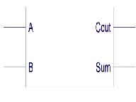
Half adder is a digital circuit that add two binary inputs and produce a sum and carry output. The two binary inputs are A and B while outputs are generally referred as Sum and Cout. The design of half adder is based on a truth table. The truth table is labeled as table 1. Figure 1
demonstrate top level symbol whereas figure 2 is a top level
schematic. Figure 3 manifest the simulation waveform.
A | B | Sum | Cout |
0 | 0 | 0 | 0 |
0 | 1 | 1 | 0 |
1 | 0 | 1 | 0 |
1 | 1 | 0 | 1 |
Table1. Half adder truth table
Figure 1.Half adder Top level symbol
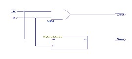
Figure 2.Top level schematic
IJSER © 2014 http://www.ijser.org
International Journal of Scientific & Engineering Research, Volume 5, Issue 3, March-2014
ISSN 2229-5518 1155
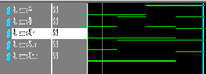
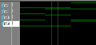
Figure 3.Half adder simulation
2.3 Full Adder
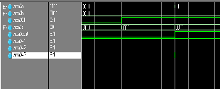
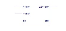
Full adder adds three binary input bits generally named as A, B, Cin and produces Sum and Carry output. Here A and B are the operands, and Cin is a bit carried from the next less significant stage. The logic of full adder is derived from truth table give in the table 2. Figure 4 represent top level symbol of full adder. Top level schematic has been shown in figure 5. Figure 6 depicts simulation waveform of the adder.
A | B | Cin | Sum | Cout |
0 | 0 | 0 | 0 | 0 |
0 | 0 | 1 | 1 | 0 |
0 | 1 | 0 | 1 | 0 |
0 | 1 | 1 | 0 | 1 |
1 | 0 | 0 | 1 | 0 |
1 | 0 | 1 | 0 | 1 |
1 | 1 | 0 | 0 | 1 |
1 | 1 | 1 | 1 | 1 |
Table 2. Full adder truth table
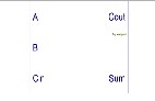
Figure 4.Full adder Top level symbol
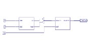
Figure 5. Full adder Top level schematic
Figure 6. Full adder simulation waveform
2.3 Ripple carry adder
Ripple carry adder is a type of a logical circuit that uses multiple numbers of full adders to add N-bit numbers. As each carry bit “ripples” through the next full adder it is referred as ripple carry adder. It is implemented with full adders connected in cascade with the carry output from each full adder connected to the carry input of the next full adder. Figure 7 depicts the top level symbol of ripple carry adder. Top level schematic has been shown in figure 8 while figure 9 shows the final simulation waveform of ripple carry adder.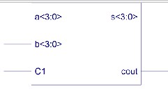
Figure 7.Ripple carry adder Top level symbol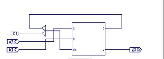
Figure 8.Ripple carry adder top level schematic
IJSER © 2014 http://www.ijser.org
International Journal of Scientific & Engineering Research, Volume 5, Issue 3, March-2014
ISSN 2229-5518 1156
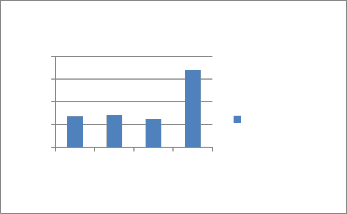
Carry select adder uses 81404 kilo bytes of memory the highest among all four while the least memory is being used by ripple carry adder. The graph in the figure 14 manifests the amount of memory utilized by the different
adders. The more the memory the larger area is required.
Figure 9. Ripple Carry adder simulation waveform
2.4 Carry select adder
Carry-select adder computes alternative results in parallel and in subsequent mode by choosing the correct result. Its area requirement is increased for enhancing the performance. Both the sum and carry bits are computed for the two alternatives: input carries ‘0’ and ‘1’. Once the
82000
81000
80000
79000
78000
Memory usage(Kilobytes)
carry-in is delivered, the correct computation is chosen to
yield the desired output. This carry select adder is of 4 bits. Simulation waveform has been shown in figure 10 whereas
topic level block and top level schematic has been shown in
Half adder
Full adder
Ripple carry adder
Carry select adder
the figure 11 and 12 respectively.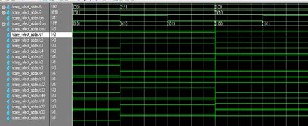
Figure 10. Carry select adder waveform
Figure 13.Memory usage by adders
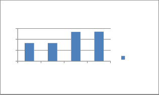
Delay indicates the time circuit takes to perform the operation. The larger the delay the slower is the circuit whereas the smaller is the delay the faster is the device. Thus on observing delay of half and full adders as 8.234 nanoseconds it is stated that they are faster than ripple carry adder and carry select adder. The graph of figure 15 shows the concept of delay.
Figure 11. Carry select adder top level symbol
15
10
5
0
Half adder
Full adder
Ripple carry adder
Carry select adder
Delay(ns)
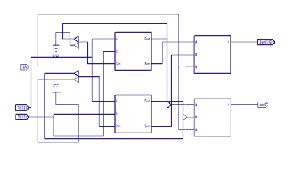
Figure 14.Delay in adders
Figure 12.Top level schematic
IJSER © 2014 http://www.ijser.org
International Journal of Scientific & Engineering Research, Volume 5, Issue 3, March-2014
ISSN 2229-5518 1157
The level of logic means the levels of combinational logic between two timing end points. If level of logic is more than devices works slower while with less level of logic device is speedy. Ripple carry adder and carry select adder both share 6 logic level, on the other hand half adder and full adder share 3 level of logic. Thus ripple carry adder
8
6
4
2
0
Number of slices
and carry select adder are slower. This is shown in figure
15.
Half adder
Full adder
Ripple carry adder
Carry select adder
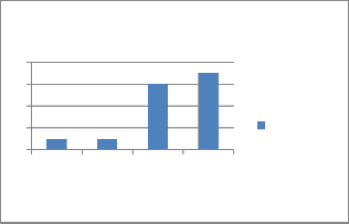

Figure 16.Figure showing number of slices used by the adders
8
6
4
2
0
Level of logic
Result has been tabled below. A comparison has been made between the four adders using four different factors namely
Half adder
Full adder
Ripple carry adder
Carry select adder
memory usage, delay, level of logic and number of slices.
Table 3 shows the various parameters.
Figure 15.Graph showing Level of logic in various adders
Slices are basic buildings blocks in FPGA. Each slice contains LUT’S, flip flops and carry logic components that make up logic of a design before mapping. After mapping is performed all LUT’s, flip flops are packed into the slices. Number of slices is used in large numbers by carry select adder, thus result in occupying larger area, more power dissipation and slower performance. This is shown in
figure 16.
Table 3.Comparison between adders
.
IJSER © 2014 http://www.ijser.org
International Journal of Scientific & Engineering Research, Volume 5, Issue 3, March-2014
ISSN 2229-5518 1158
The four adders namely half adder, full adder, ripple carry
adder and carry select adder has been design and four major factors contributing in the area, power dissipation and performance has been compared. The compared parameters are memory, delay, level of logic and number of slices. The result suggests that among the two adders compared half adder and full adder consumes equal amount of power, equal lesser area. Among ripple carry adder and carry select adder, ripple carry adder is slightly better in area, performance and power dissipation. Overall carry select adder is worst in case of delay, power consumption and area.
[1] Padma Devi, Ashima Girdher, Balwinder Singh ,” Improved Carry Select Adder with Reduced Area and Low Power Consumption “International Journal of Computer Applications (0975 – 8887) Volume 3 – No.4, June 2010
[2] M.Chithra, G.Omkareswari, “128-BIT CARRY SELECT ADDER HAVING LESS AREA AND DELAY”, International Journal of Advanced Research in Electrical, Electronics and Instrumentation Engineering , Vol. 2, Issue 7, July 2013
[3] J R Padmasri, Christina P A, Kavitha. P & T. Mullai,“ Modified Area Efficient Carry Select Adder (MA-CSLA) “ , International Journal of Advanced Electrical and Electronics Engineering (IJAEEE), ISSN (Print) : 2278-8948, Volume-2, Issue-2, 2013
[4] Behnam Amelifard, Farzan Fallah, and Massoud Pedram, "Closing the gap between carry select adder and ripple carry adder: a new class of low-power high-performance adders", in Proc. of IEEE International Symposium on Quality Electronic Design (ISQED), 2005.
Anuj, student B.Tech (completed) at T.C.M College of engineering, Gannaur in Electronics and Communication discipline. His main area of interest is Digital system design
using VHDL, Verilog HDL and Low power VLSI system.
IJSER © 2014 http://www.ijser.org