International Journal of Scientific & Engineering Research Volume 2, Issue 10, October-2011 1
ISSN 2229-5518
Achieving Zero Common Mode Voltage and Improved Linearity Relationship by a Novel Modulation Method
Nasim Rashidirad, Abdolreza Rahmati, Adib Abrishamifar
Abstract—This paper proposed a new modulation strategy to eliminate common mode voltages in multilevel inverters. In this scheme which is explained for a 5-level modular inverter, all voltage vectors with zero common mode voltages can be classified into four categories and each two adjacent categories composed a segment. Synthesized voltage vectors that are an approximation to the reference vector belong to the segment in which the reference vector lies. Dwell times of these voltage vectors, depend on the distance between reference vector and the voltage vectors. This scheme leads to a good linearity relationship and low total harmonic distortion.
Index Terms— Common mode voltage, Multilevel modular inverter, Modulation, Linearity, THD
—————————— ——————————
1 INTRODUCTION
The main purpose of the control for multilevel inverters is to synthesize the output voltages corresponding to the desired sinusoidal waveforms. Many modulation schemes have been developed with considerations to harmonic generation, linearity relationship or common mode voltage eliminations [1-3]. Due to the resulting overall inverter performance, simplicity both in hardware and software, space vector modulation is still considered as a suitable choice for multilevel PWM inverters [4].
One of the simplest ideas to control the output voltages based on SVM is to select adjacent voltage vectors. The dwell times of these vectors is based on time-averaging principle which may lead to complicated calculations. In some schemes to achieve simpler calculations, only nearest vector to the reference vector will be delivered [1,
5]. Figure 1(a) shows a modular five-level PWM inverter. Each leg consists of four bidirectional chopper-cells which have been shown in figure 1(b).
These cells which are the basic components of the MMC
topology known as a sub-module. Each sub-module consists of a dc capacitor and two IGBTs which composed a bidirectional chopper. Its output voltage is
————————————————
N. Rashidi-rad, Iran University of Science and Technology, Iran, E-mail: Nasim83.iust@gmail.com
A. Rahmati, Iran University of Science and Technology, Iran, E-mail:
rahmati@iust.ac.ir
A. Abrishamifar, Iran University of Science and Technology, Iran, E-mail:
Abrishamifar@iust.ac.ir
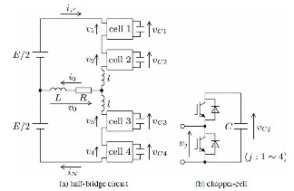
either equal to the capacitor voltage Vc or zero. Also it should be noted that to avoid short-circuiting, operation of the switches has a complementary role in a sub- module. So when either of the sub-modules is turned-on, the other one of the same sub-module must be switched off. Since the number of chopper-cells per leg is four, five-level (9-level in line-to-line) PWM waveforms will be produced.
Figure 1. circuit configuration of a modular multilevel converter
2 PROPOSED MODULATION ALGORITHM
One of the easiest space vector modulation methods is to deliver the nearest voltage vector with respect to the reference vector [1]. Figure 2 represents the phase voltages, line to line voltage, and common mode voltage in a five-level inverter controlled by this scheme (using
IJSER © 2011 http://www.ijser.org
International Journal of Scientific & Engineering Research Volume 2, Issue 10, October-2011 2
ISSN 2229-5518
nearest vectors), operating with a modulation index of m=.9 and fundamental frequency of 50Hz. Considering figure 2 (b) this modulation method generates an important amount of common mode voltages. Common mode voltages commutations can generate circulating currents that is the cause of bearing failures [6]. Therefore, to avoid these failures, this scheme is not recommended.
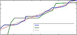
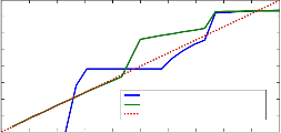
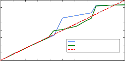
increased. Consequently as shown in figure 3, the linear relationship between fundamental voltage and modulation index will be decreased [1]. The proposed method in this paper, will completely eliminate common mode voltages, and will improve the linear relationship.
4
3.5
3
2.5
2
1.5
1
0.5
0
using ne arest ve ctors
using ne arest ve ctors with V com=0
ide al
0.2 0.3 0.4 0.5 0.6 0.7 0.8 0.9 1
Index Modulation
Figure 3. Comparsion of fundamental voltage (a1) versus index modulation (m) in a 5-level inverter (1pu=Vcc)
(a)
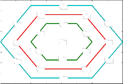
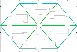
In the proposed method, voltage vectors with zero common mode voltages are classified into four categories and each category is located on a hexagonal in space vector diagram as shown in figure 4. It should be noted that the zero voltage vector (2, 2, 2) by itself is a category.
4
(b)
(c)
3
2
042
1
033
-1
-2 024
-3
-4
141
132
123
114
240
231
222
213
204
330
321
312
303
420
411
402
-4 -3 -2 -1 0 1 2 3 4
Figure 4. Representation of voltage vectors with zero common mode in a five-level inverter.
(d)
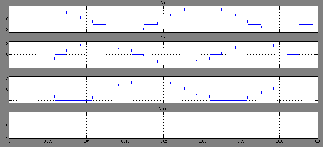
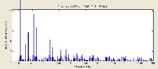
Figure 2. (a) Phase voltages, (b) common mode voltage, (c) line to line voltage, and (d) spectrum of line to line voltage in a five level inverter using nearest vectors method with m=.9
To modify this scheme, only voltage vectors which have zero common mode voltages can be used. This restriction of vectors increases the distance between reference vector and the vectors of space vector diagram. So the error of
the generated voltage with respect to the reference will be
Each of categories creates a circle. Therefore as shown in figure 5, circles with radiuses R1 and R3 have been embeded in green and blue hexagonals respectively. Second hexagonal that is red colored, has been embebed in the circle with radius R2.
It should be noted that the first category which is a zero vector, is a circle with zero radius, (i.e. a simple dot). Each two adjacent circles compose a segment as shown in Table 1. Thus d-q plane is divided into 3 segments.
Considering table 1, each of centric circles with R1 and R2 radiuses has been used in two segments. Therefore to
IJSER © 2011 http://www.ijser.org
International Journal of Scientific & Engineering Research Volume 2, Issue 10, October-2011 3
ISSN 2229-5518
specify the border of each segment it should be determined that reference vector is closer to which of adjacent circles.
the desired voltage vector. the dwell times of these vectors depend on distance between reference vector and them. To determine the dwell times, parameter m is
defined as:

4
Vref
m
2
i
R1
60

2
(3)
1
0 R3 R0
-1 R2
-2
-3
-4
-4 -3 - 2 -1 0 1 2 3 4
The main idea of this scheme is based on specifying
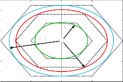
2m of each sector as shown in figure 6, to the voltage vectors which are located on circle with radius Ri. The residue of sector is specified to the vectors of other circle which is composed the segment. So if the reference vector will be closer to circle with radius Ri, the section of sector
which is dedicated to this circle will be greater.
Figure 5. Representation of circles with radiuses R0, R1, R2 and R3
4
TABLE 1
TWO ADJACENT CIRCLES IN EACH SEGMENT
3
141
2
240
sector 2
330
042
1
0 033
sector 3
132
231 sector 1
321
222
420
411
-1
024
-3
sector 4
123
114
213
sector 5
204
312
303
sector 6
402
-4
-4 -3 -2 -1 0 1 2 3 4
For example to determine the border of segment 1:
Figure 6. Representation of sectors and voltage vectors in each sector.

Vref
So :


R0

Vref


R2


Vref

R0 R2
2
(1)
3 SIMULATION RESULTS
the waveform of figure 7 has been measured with m=.9 and an output frequency of 50Hz. Switching frequency is
5kHz.

if V

ref

R0 R2
2
segment1
Figure 8 represents a comparsion of THD diagram between previous and proposed methods while both of

if R0 R2  V
V
2

ref

R1 R3
2
segment 2
(2)
them eliminate common mode voltages. Considering figure 8, THD diagram in mentioned schemes is similar

if R1 R3  V
V
2

ref
segment 3
especially at higher modulation indexes.
Figure 9 shows the comparsion of linearity relationship
When the reference vector falls in one of the segments the voltage vectors in that segment are selected to synthesize
between two mentioned methods. One of the disadvantage of previous method is to have zero
fundamental voltage up to m=.25 which is removed by
IJSER © 2011 http://www.ijser.org
International Journal of Scientific & Engineering Research Volume 2, Issue 10, October-2011 4
ISSN 2229-5518
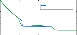
the proposed method. Considering this figure it can be concluded that the linearity of proposed method is better than the previous method.
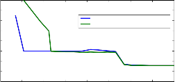
modulation indexes. Also because of the steep slope in the second segment, its margin can be decreased. Finally as shown in figures 10 and 11, the relationship will be more linear while THD diagram will have small variations compared to the former proposed method.
4
3.5
3
2.5
2
(a)
1.5
1
0.5
0
using ne arest v ectors with V com=0 proposed method
ideal
(b)
0 0.1 0.2 0.3 0.4 0.5 0.6 0.7 0.8 0.9 1
Index Modulation
Figure 9. Comparsion of fundamental voltage (a1) versus modulation index (m) in a five-level inverter (1pu=Vcc).
4
3.5
3
2.5
2
1.5
1
0.5
propose d me thod
improv ed proposed method ide al
0
0 0.1 0.2 0.3 0.4 0.5 0.6 0.7 0.8 0.9 1
Index Modulation
(c)
Figure 7. (a) Phase and common mode voltages, (b) line to line voltage, and (d) spectrum of line to line voltage in a five level inverter using proposed method with m=.9
Figure 10. Comparsion of fundamental voltage (a1) versus modulation index (m) in a five-level inverter (1pu=Vcc)
120
100
80 80
proposed method
improved proposed method
70 60
60 using ne arest ve ctors with V com=0
proposed me thod 40
50
40 20
30 0
0.2 0.3 0.4 0.5 0.6 0.7 0.8 0.9 1
20 Index Modulation
10
0
0.2 0.3 0.4 0.5 0.6 0.7 0.8 0.9 1
Index Modulation
Figure 8. Comparsion of total harmonic distortion (THD) versus modulation index (m) in a five-level.
To improve the linearity relationship in the proposed method, the margin of the first segment can be decreased. Applying this change will lead to a smaller jump in lower
Figure 11. Comparsion of total harmonic distortion (THD) versus modulation index (m) in a five-level inverter
4 CONCLUSION
This paper proposed a new SVM scheme to eliminate common mode voltages in multilevel inverters. In this scheme, the space vectors are restricted to vectors with
zero common mode voltages and are classified into four
IJSER © 2011 http://www.ijser.org
International Journal of Scientific & Engineering Research Volume 2, Issue 10, October-2011 5
ISSN 2229-5518
categories. Except the first category which has a zero voltage vector, the next ones have six voltage vectors located on three hexagonals. Each two adjacent categories composed a segment that their vectors are used to synthesize the reference vector. So each segment has two categories of vectors, and the dwell times of them are depend on the distance between reference vector and these vectors. This scheme has a good linearity relationship and low total harmonic distortion.
REFERENCES
[1] Jose Rodriguez, Jorge Pontt, Pablo Correa, Patricio Cortes, Cesar Silva, “A New Modulation Method to Reduce Common-Mode Voltages in Multilevel Inverters”, IEEE TRANSACTIONS ON INDUSTRY ELECTRONICS, VOL.51, NO.4, AUGUST 2004.
[2] Shaotang Chen, Thomas A.lipo, Dennis Fitzgerald, “Modeling of Motor Bearing Currents in PWM Inverter Drives”,IEEE TRANSACTIONS ON INDUSTRY APPLICATIONS, VOL. 32, NO.
6, NOVEMBER/ DECEMBER 1996.
[3] “Don’t Lose Your Bearings, Mitigation techniques for bearing currents in inverter-supplied drive systems”, IEEE INDUSTRY APPLICATIONS MAGAZINE, JULY/AUG 2006.
[4] Wenix Yao, Haibing Hu, Zhengyu Lu, “ Comparsions of Space- vector Modulation and Carrier-Based Modulation of Multilevel Inverter”, IEEE TRANSACTIONS ON POWER ELECTRONICS, VOL. 23, NO. 1, JANURAY 2008.
[5] Haoran Zhang, Annette von Jouanne, Shaoan Dai, Alan K.Wallace, Fei Wang, “Multilevel Inverter Modulation Schemes to Eliminate Common-Mode Voltages”, IEEE TRANSACTIONS ON INDUSTRY APPLICATIONS, VOL. 36, NO. 6, NOVEMBER / DECEMBER 2000.
[6] Shaotang Chen, Thomas A.lipo, Dennis Fitzgerald, “Modeling of Motor Bearing Currents in PWM Inverter Drives”, IEEE TRANSACTIONS ON INDUSTRY APPLICATIONS, VOL.32,
NO. 6, NOVEMBER/DECEMBER 1996.
IJSER © 2011 http://www.ijser.org