
International Journal of Scientific & Engineering Research, Volume 4, Issue 4, April‐2013 1220
ISSN 2229‐5518
A Three Phase Five Level Inverter with Coupled
Inductor Using SVPWM
S.Vigneshwaran, Dr.SP.Umayal
Abstract— PWM are widely applied in many industrial applications that require notable performance. Lately, developments in power electronics drives and semiconductor technology have lead amendments in power electronic systems. Hence, distinct circuit configurations namely multilevel inverters have become trendy and considerable interest by researcher are given on them. Variable frequency and voltage supply to a.c drives is consistently obtained from a three-phase voltage source inverter. A number of Pulse width modulation proposals are used to obtain variable frequency and voltage supply. The most widely used PWM schemes for three-phase voltage source inverters are sinusoidal PWM and space vector PWM (SVPWM). There is an rising trend of using space vector PWM (SVPWM) because of their easier digital realization and better dc bus utilization. This project focuses on A Three phase 5-Level Inverter with coupled inductor using SVPWM . The archetypal of a three-phase a voltage source inverter is discussed based on space vector concept. Simulation results are obtained using MATLAB/ Simulink environs for value of the study.
Index Terms— Multilevel Inverters, power converters, pulse width modulation, three-phase inverter, Coupled inductor.
—————————— ——————————
INCE their beginning, multilevel inverters (MLI) have been receiving much attention and as a result many different topologies have been proposed. The academic papers and theses focusing on MLI topologies are almost innumerable. These MLI topologies can be classified according to many criteria. This paper will focus on three-
phase multilevel inverters.
A novel single-phase five-level inverter using coupled
inductors and the common three-arm power module [1].For
single-phase MLI, the most common topologies are the
cascaded, diode-clamped, and capacitor clamped types [2]–
[3]. There occur many other topologies [4]–[26]. In general,
MLI topologies can be classified into two types: Type I and
Type II. Type I uses numerous dc voltage sources and Type II
uses numerous (split or clamping) dc voltage capacitors. Type
I includes the conventional cascaded topologies [1]–[3], those
presented in [4]–[8] and so forth. Type II includes the
traditional diode-clamped, capacitor-clamped inverters, the
topologies proposed in [9]–[26]. In terms of single phase
multilevel inverters, the disadvantages of the two types are
obvious. Type I suffers from the availability of the numerous
dc voltage sources. In practice, bulky transformers either of
low or medium frequency are usually necessary if a Type I
inverter is elected. This is a great task to when it comes to
volume, weight, and cost minimization. The problem with
Type II is mainly the balancing of the dc capacitor voltages,
though some MLI topologies can achieve self-balancing with
certain control algorithms.
A MLI with only one dc source and no split capacitors may be
————————————————
S.Vigneshwaran is currently pursuing Masters degree program in Power Electronics and Drives in Sethu Institute Of Technology, Kariyapatti, India. E-mail: svigneshwaran2@gmail.com
Dr.SP.Umayal working as Professor and head in the department of M.E- Power Electronics And Drives at Sethu Institute Of Technology, Kariyapatti, India. E-mail: umayalbabu@gmail.com
the most desirable topology but unfortunately this type of inverter has yet to be discovered. Recently, MLI with coupled inductors have drawn some researchers’ interest and a half- bridge 3-level inverter has been intended using two power switches, two diodes, and two coupled inductors [27]– [30].Whereas, as for single-phase five-level cases, two such half-bridges, i.e., six power and four coupled inductors will be needed [28], [29]. What is more, dc component exists in the inductor current in these of inverters, which is dangerous to the full use of the magnetic cores.
More lately, [31] presented a single-phase inverter called a five-level-active-neutral-point clamped with coupled inductor (5L-ANPC-CI). The 5L-ANPLCI inverter uses eight power switches, and split of the dc-link capacitor is essential. Thus, the risk of unbalanced capacitor voltage exists if the inverter is not correctly modulated.
Also a novel single-phase five-level inverter using coupled inductors and the common three-arm power module. With this newly emerged inverter, only one dc voltage source is needed and split of the dc voltage capacitor is also avoided, which avoids the problem of dc capacitor voltage balancing with the traditional topologies. Meanwhile, six power switches with the same voltage stress and only one set of coupled inductors are elected. Also, less inductor is needed in the inverter intended in this paper compared with the topology in [28] and [29].
Three phase voltage-fed PWM inverters are in lately times showing growing fame for multi-megawatt industrial drive applications. The main reasons for this esteem are easy sharing of large voltage between the series devices and the amendment of the harmonic quality at the output as compared to a two level inverter. In the inferior end of power, GTO devices are being replaced by MOSFET’s because of their rapid evolution in voltage and current ratings and higher switching frequency.
The model of A Novel Three phase 5-Level inverter is
discussed based on space vector theory for adjustable speed
drives. Simulation results are obtained using
MATLAB/Simulink environs for value of the study.
IJSER © 2013 http://www.ijser.org
International Journal of Scientific & Engineering Research, Volume 4, Issue 4, April‐2013
ISSN 2229‐5518
1221
vector modulation concepts. As time rises, the
angle of the
Fig. 1 shows the circuit of the proposed three-phase five level
space
vector rises, causing the vector to spin with frequency
inverter. In Fig. 1, E is the dc-link voltage and L1 and L2 are
equal
to the frequency of the
sinusoids. A three phase
the two coupled inductors. The mutual inductance of the two
system
defined by
Va(t), Vb(t),
Vc(t) can be
represented
inductors is M and the output terminals of this inverter are1
uniquely by a spining vector,
(the same point as the output of arm a) and 2. Obviously, this topology is very simple and can be constructed simply by adding two coupled inductors to a conventional three-arm inverter bridge.
Where ,
ࢂࢉ (t )ࢋି࣊/
(1)
Va (t) =
Vb (t) =
Vm sinωt
Vm sin(ωt-2π/3)
Vc (t) = Vm sin(ωt+2π/3)
In space vector pulse width modulation technique, the three
phase stationary reference frame
voltages or
each inverter
switching state are
charted to
the complex two phase
orthogonal α-β plane. The mathematical transmute for
converting the stationary three
phase parameters to the
It is, in fact, the adoption of the coupled inductors that makes
orthogonal plane is known as the Clark ’s transformation. The reference voltage is signified as a vector in this plane. In a three-phase system, the vectorial illustration is achieved by the transformation given in Fig. 2.
it possible to output five-level voltage with only one dc
voltage source. So the role of the coupled inductors will be analyzed first. Suppose that the two coupled inductors are with the same number of turns or obtained by a center-tapped inductor. This result is interesting and shows that the coupled inductors will perform as an adder of the two input voltage at
ence on of
the
non-common-connected terminals with
the common-
The vector recognition uses a ‘0’ to signify the negative phase
connected terminal as the output. Actually, without the help of the coupled inductors, the proposed inverter will not be able to output five-level voltage.
The SVM is a classy, averaging algorithm which gives 15% more voltage output compared to the Sinusoidal PWM algorithm, thereby rising the Vdc utilization. It also reduces the THD as well as switching loss. Like Sinusoidal PWM, the SVM is similarly a scalar control. The three-phase line-to- neutral sine waves required for driving the 3-phase induction motor can be represented as 120° phase-shifted vectors.
For a balanced 3-phase system, these vectors add to zero.
voltage level and ‘1’ to represent the positive phase voltage
level. Six non-zero vectors (V1 and V6) shape the axis of
hexagonal and the angle between any adjacent two non-zero
vectors is 60 .
Two of these states (V0 and V7) correspond to a short circuit on the output, while the other six can be considered to form stationary vectors in the α-β complex plane as shown in Fig. 3. The eight vectors are called the basic space vectors.
Therefore, they
can be expressed as
a single space
reference vector.
By controlling the amplitude and he
frequency of r e f er ence vector , the motor voltage and the
motor frequency
can be precise. Hence, this algorithm is
known as the SVPWM.
Any three time varying quantities, which always sum to
zero and are spatially detached by 120° can be expressed space
IJSER © 2013 http://www.ijser.org
International Journal of Scientific & Engineering Research, Volume 4, Issue 4, April‐2013
ISSN 2229‐5518
1222
Each stationary vector corresponds to a particular fundamental angular position as shown in Fig. 4. An arbitrary target output voltage vector, Vref is formed by the summation of a number of
The six active-vectors are of equal magnitude and are mutually phase displaced by π/3. The general articulation can
these space vectors within one
switching period, which is
be represented by,
shown in Fig.5 for a target phasor in the first 60 segment
of the plane.
Any space vector lies in the hexagon can be composed by
time averaging of the adjacent two active space vectors and
zero vectors. For each switching period Ts,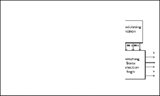
ܸ ൌ ܸ . ݁ሺିଵሻగ/ଷ ,݊ ൌ 1,2 … 6
ion
(5)
Any space vector lies in the hexagon can be composed by time averaging of the adjacent two active space vectors and zero vectors. For each switching period Ts,
The duty cycle calculation is done for each triangular sector formed by two state vectors. The individual duty cycles for each sector boundary state vectors and the zero state vector are given by,
்௦ ்ଵ
்ଶ ்ଶ
ܸݎ݂݁ ݀ݐ ൌ
ܸ1 ݀ݐ ்ଵ ܸ2 ݀ݐ ்ଵ ܸ0 ݀ݐ
(6)
݀_ߙ ൌ ܸ_ݎ݂݁/ܸ_ܦܥ . ሺሾsin ሺሺߨ/3ሻ െ ߠሻ ሿ/sin ߨ ሻ/3
ming up of
the geometric summing up can be articulated mathematically as
ܸ ൌ ܸ ݈ܽ݊݃݁ߠ
ൌ ݉ sinሺሺߨ /3ሻ െ ߠሻ
݀_ߚ ൌ ܸ_ݎ݂݁/ܸ_ܦܥ . ሼsin ߠ/ሾsinߨ/3ሿሽ ൌ ݉sin ߠ
݀_0 ൌ 1 െ ݀_ሺߙ െ ݀_ߚ ሻ
where,
(7) (8) (9)
ൌ ቀ ்భ ቁ.ܸ ቀ ்మ ቁ.ܸ ቀ்బቁ.ܸ
(2)
݀_ߙ ൌ ܶ_1/ܶ_ݏ,
݀_ߚ ൌ ܶ_2/ܶ_ݏ, ![]()
![]()
![]()
்ೄ ଵ
்ೄ ଶ
்ೞ
݀_0 ൌ ܶ_0/ܶ_ݏ
where, T1 is the time for which space vector V1 is selected and T2 is the time for which space vector V2 is selected. The block diagram for generating SVM pulses is shown in Fig.6. SVM can be instigated through the following steps:
The space vector, Vref is normally represented in complex plane and the magnitude as,
This gives switching times T 0, T1 and T2 for each inverter state for a total switching period, Ts. Applying both active and zero vectors for the time periods given in (6) ensures that average voltage has the same magnitude as desired.
The four modulating functions, m0, m1, m2 and m3, in terms of the duty cycle for the space vector PWM scheme can be expressed as,
|ܸ_ݎ݂݁ | ൌ √ሺܸ_ߙ^2 ܸ_ߚ^2 ሻ
ߠ ൌ tan^ሺെ1ሻ ሺܸߚ/ܸߙሻ
Where,
(3)
(4)![]()
݉_0= ݀ 0/2
݉_1= ݉_ ݀_ߙ
݉_2 ൌ ݉_1 ݀_ߚ
(10) (11)
(12)
ܸఈ ൌ ܸ cos ߠ,
ܸఉ ൌ ܸ sin ߠ
݉_3 ൌ ݉_0 ݀_ߚ
IJSER © 2013 http://www.ijser.org
(13)
International Journal of Scientific & Engineering Research, Volume 4, Issue 4, April‐2013
ISSN 2229‐5518
1223
substantial decrease
of the dv/dt in the inverter output
The
required pulses can be
initiated by
comparing
the
voltage.
modulating functions with t
he triangular waveform. A
symmetric seven segment technique is to alternate the null vector in each cycle and to contrary the sequence after each null vector. The switching pulse pattern for the 3 phases in
the six sectors can be initiated. A typical
seven segment
switching sequence for generating reference vector in sector one is shown in Fig. 7.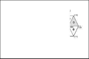
In order to verify the validity of the topology with
the
inverter.
optimized modulation scheme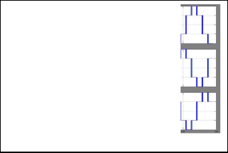
in this paper, the intended
inverter is tested with series-connected RL load. The load resistor is RL and the load inductor is LL. A three-phase inverter with a balanced star connected RL load is considered. A complete mathematical model of the SVPWM is developed
and
simulated using MATLAB/Simulink to
investigate
the
performance of
a three phase inverter.Fig.8. shows the
sector selection algorithm.

In this
paper, mathematical archetypal of a
space vector
modulated three phase inverter using MATLAB/Simulink.
is orginated and simulated
Also
Space Vector PWM is
unique as
compared to
Sinusoidal pulse width modulation in many aspects like:
The output voltage is about 15% more in case of SVPWM
as compared to Sin-PWM.
The current harmonics produced are much less in case of
SVPWM.
Sector corresponds to the
location of voltage in
the
With the increased
output voltage, the user can sketch
circular locus traced by it and is divided into six sectors of
the motor control system with
decreased current rating,
60° each which is shown in Fig. 9 and line voltages are shown
which
helps to decrease inherent conduction loss of the
in Fig.10. Fig.11
shows the line current, because of
the
voltage
source inverter. However despite
all the above
inductive nature of the load,
higher order
harmonics have
mentioned advantages that SVPWM enjoys over Sin-
been potable out and the current waveform
is sinusoidal in
PWM, SVPWM algorithm used in 3-level inverters is more
nature. What is more, in all these simulations, the height of
complex because of
large number of inverter switching
the
staircase in
the output
voltage is 88V in five-level
states. Hence we see that there is a certain trade off that exists
condition. Compared with the H-bridge inverter, this is a
while using SVPWM for inverters for Adjustable speed Drive
IJSER © 2013 http://www.ijser.org
International Journal of Scientific & Engineering Research, Volume 4, Issue 4, April‐2013
ISSN 2229‐5518
1224
Operations. Also the use of a coupled inductor is described to allow interleaved pwm switching of the upper and lower switches in an inverter leg. This increases the number of pwm output voltage levels and doubles the pwm frequency. The main advantages of this topology are:
Multi-level pwm (3-level increased to 5-level) using half
the power electronics of alternative schemes. The ac filter
inductor can be reduced in size. The fundamental voltage
drop across the inductor is also reduced as a result and more
fundamental voltage reaches the load. The switch control
deadtimes can be eliminated, helping to improve the quality
of the pwm voltage generation and increasing the maximum
potential output voltage. The coupled inductor provides
excellent protection against dc-rail shoot-through conditions.
[1] Zixin Li, Ping Wang, Yaohua Li, and Fanqiang Gao, “A novel single phase five level inverter using coupled inductors,” IEEE Trans. Ind. Electron., vol.
27, no. 6,, June. 12.
[2] M..Malinowski, K. Gopakumar, J. Rodriguez, and M. A. Perez, “A survey on cascaded multilevel inverters,” IEEE Trans. Ind. Electron., vol. 57, no. 7, pp. 2197–2206, Jul. 10.
[3] J. Rodriguez, S. Bernet, P. K. Steimer, and I. E. Lizama, “A survey on neutral- point-clamped inverters,” IEEE Trans. Ind. Electron., vol. 57, no. 7, pp. 2219–
2230, Jul. 2010.
[4] Y.-S. Lai and F.-S. Shyu, “Topology for hybrid multilevel inverter,” IEEE Proc. Electron. Power Appl., vol. 149, no. 6, pp. 449–458, Nov. 02.
[5] Y. Hinago and H. Koizumi, “A single-phase multilevel inverter using switched series/parallel DC voltage sources,” IEEE Trans. Ind. Electron., vol.
57, no. 8, pp. 2643–2650, Aug. 10.
[6] H. Akagi and R. Kitada, “Control and design of a modular multilevel cascade BTB system using bidirectional isolated DC/DC converters,” IEEE Trans. Power Electron., vol. 26, no. 9, pp. 2457–2464, Sep. 11.
[7] Y.-H. Liao and C.-M. Lai, “Newly-constructed simplified single-phase Multi string multilevel inverter topology for distributed energy resources,” IEEE Trans. Power Electron., vol. 26, no. 9, pp. 2386–2392, Sep. 11.
[8] J. Shi, W. Gou, H. Yuan, T. Zhao, and A. Q. Huang, “Research on voltage and power balance control for cascaded modular solid-state transformer,” IEEE Trans. Power Electron., vol. 26, no. 4, pp. 1154–1166, Apr. 11.
[9] F. Z. Peng, “A generalized multilevel inverter topology with self voltage balancing,” IEEE Trans. Ind. Appl., vol. 37, no. 2, pp. 611–618, Jul. 01.
[10] Y. Ounejjar and K. Al-Haddad, “A novel high energetic efficiency multilevel
topology with reduced impact on supply network,,” in Proc. IEEE 34th Ann. Conf. Ind. Electron. (IECON), 08, pp. 489–494.
[11] S.-J. Park, F.-S. Kang, M. H. Lee, and C.-U. Kim, “A new single-phase five-
level PWM inverter employing a deadbeat control scheme,” IEEE Trans. Power Electron., vol. 18, no. 3, pp. 831–843, May 03.
[12] G. Ceglia, V.Guzman, C.Sanchez, F. Ibanez, J.Walter, and M.I. Gimenez, “A
new simplified multilevel inverter topology for DC–AC conversion,” IEEE Trans. Power Electron., vol. 21, no. 5, pp. 1311–1319, Sep. 06.
[13] L.Chen,L. Hu,L. Chen,Y. Deng and X. He ,”A Multilevel Converter topology
with fault tolerant ability,”IEEE Trans. Power Electron. Vol.20, no. 2, pp.405-
415, Mar. 05.
[14] A.Chen and X. He,”Research on hybrid- clamped MLI topologies,” IEEE ,” IEEE Trans. Ind. Electron., vol. 53, no. 6, pp. 1898–1907,Dec..06.
[15] G.-J.Su,”Multilevel dc-link Inverter,” IEEE Trans. Ind. Appl., vol. 41, no. 3, pp.
848-854, May 05.
[16] F.-P. Zeng, G.-H.Tan, J.Z.Wang, and Y.-C. Ji, “Novel single-phase five level voltage-source inverter for the shunt active power filter,” IET Power Electron., vol. 3, pp. 480–489, 10.
[17] Z. Du, L. M. Tolbert, J. N. Chiasson, and B. Ozpineci, “A cascade multilevel inverter using a single DC source,” in Proc. IEEE Appl. Power Electron. Conf. (APEC), 06, pp. 426–430.
[18] Z. Du, B. Ozpineci, L. M. Tolbert, and J. N. Chiasson, “DC–AC cascaded H- bridge multilevel boost inverter with no inductors for electric/hybrid electric vehicle applications,” IEEE Trans. Ind. Appl., vol. 45, no. 3, pp. 963–970, May/Jun. 09.
[19] M. Glinka, “Prototype of multiphase modular-multilevel-converter with
2MW power rating and 17-level-output-voltage,” in Proc. IEEE Power
Electron. Spec. Conf. (PESC), 04, pp. 2572–2576.
[20] M. Glinka and R.Marquardt, “A new AC/AC multilevel converter family,” IEEE Trans. Ind. Electron., vol. 52, no. 3, pp. 662–669, Jun. 05.
[21] M. Hagiwara and H. Akagi, “Control and experiment of pulse width modulated modular multilevel converters,” IEEE Trans. Power Electron., vol.
24, no. 7, pp. 1737–1746, Jul. 09.
[22] S. Rohner, S. Bernet, M. Hiller, and R. Sommer, “Modulation, losses, and semiconductor requirements of modular multilevel converters,” IEEE Trans. Ind. Electron., vol. 57, no. 8, pp. 2633–2642, Aug. 10.
[23] A. Nami, F. Zare, A. Ghosh, and F. Blaabjerg, “A hybrid cascade converter topology with series-connected symmetrical and asymmetrical diode clamped h-bridge cells,” IEEE Trans. Power Electron., vol. 26, no. 1, pp. 51–
65, Jan. 11.
[24] J. Li, S. Bhattacharya, and A. Q. Huang, “A new nine-level active NPC(ANPC) converter for grid connection of large wind turbines for distributed generation,” IEEE Trans. Power Electron., vol. 26, no. 3, pp. 961–
972, Mar. 11.
[25] P. P. Rajeevan, K. Sivakumar, C. Patel, R. Ramchand, and K.Gopakumar, “A seven-level inverter topology for induction motor drive using two level inverters and floating capacitor fed H-bridges,” IEEE Trans. Power Electron., vol. 26, no. 6, pp. 1733–1740, Jun. 11.
[26] J. Zhao, Y. Han, X. He, C. Tan, J. Cheng, and R. Zhao, “Multilevel circuit topologies based on the switched-capacitor converter and diode-clamped converter,” IEEE Trans. Power Electron., vol. 26, no. 8, pp. 2127–2136, Aug.
11.
[27] A. M. Knight, J. Ewanchuk, and J. C. Salmon, “Coupled three-phase inductors for interleaved inverter switching,” IEEE Trans.Magn., vol. 44, no.
11, pp. 4199–4122, Nov.08.
[28] J. Salmon, A. Knight, and J. Ewanchuk, “Single phase multi-level PWM inverter topologies using coupled inductors,” in Proc. IEEE Power Electron. Spec. Conf. (PESC), 08, pp. 802–808.
[29] J. Salmon, J. Ewanchuk, and A. M. Knight, “PWM inverters using split wound coupled inductors,” IEEE Trans. Ind. Appl., vol. 45, no. 6, pp. 2001–
2009, Nov. 09.
[30] C. Chapelsky, J. Salmon, and A. M. Knight, “Design of the magnetic components for high-performance multilevel half-bridge inverter legs,” IEEE Trans. Magn., vol. 45, no. 10, pp. 4785–4788, Oct. 09.
[31] D. Floricau, E. Floricau, and G. Gateau, “New multilevel converters with coupled inductors: Properties and control,” IEEE Trans. Ind. Electron., vol. 58, no. 12, pp. 5344–5351, Jul. 11.
IJSER © 2013 http://www.ijser.org