International Journal of Scientific & Engineering Research Volume 2, Issue 12, December-2011 1
ISSN 2229-5518
A Survey of Cluster Based Multi-Processor system design with IP-Cores
K. Immanuvel Arokia James
Abstract— This project aims to design a cluster-based multiprocessor system-on-chip (MPSoC) combines of hybrid interconnection composed of both bus based and network on chip (NOC) architecture. Two or more microprocessors working together to perform one or more related tasks using a shared memory is commonly referred to as a multiprocessor system. NoC is used to form a network to pass the message packets more efficiently between the source and destination and to provide additional communication resources so that multiple paths can be operated simultaneously. High performance is achieved by efficient implementation of hardware and software. It is done by fine tuning MPSoC architecture in the early stage of the design process. This project uses the FPGA device to prototype the cluster-based MPSoC. This paper proposes a hierarchical architecture consisting of SMP clustered nodes, each of which is structured by more than one baseline cores through centrally-shared memory and, some parallel applications with different characteristic of parallelism, functionality and communication pattern are designed and presented in this work. In this work a pure VHDL design, integrated with some intellectual property (IP) blocks. This project accounts for the highest throughput ratio.
Index Terms — MPSoC, Cluster, IP Cores, NoC.
—————————— ——————————
1 INTRODUCTION
ny system that incorporates two or more microproces- sors working together to perform one or more related tasks is commonly referred to as a multiprocessor sys-
tem. In a multiprocessing system, all CPUs may be equal, or some may be reserved for special purposes. A combina- tion of hardware and operating-system software design considerations determines the symmetry in a given system. For example, hardware or software considerations may require that only one CPU respond to all hardware inter- rupts, whereas all other work in the system may be distri- buted equally among CPUs; or execution of kernel-mode code may be restricted to only one processor (either a spe- cific processor, or only one processor at a time), whereas user-mode code may be executed in any combination of processors. Multiprocessing systems are often easier to de- sign if such restrictions are imposed, but they tend to be less efficient than systems in which all CPUs are utilized. Systems that treat all CPUs equally are called symmetric multiprocessing (SMP) systems. Because of the flexibility of SMP and because of its cost being relatively low, this archi- tecture has become the standard for mainstream multipro- cessing.
K. Immanuvel Arokia James is pursuing PhD in VEL TECH Dr. RR & Dr. SR Technical University, Chennai. He is currently working as a Assis- tant Professor in Department of Electrical and Electronics Engineering at VEL Tech Multi Tech Dr. RR and Dr. SR Engineering College affiliated to Anna University, Chennai. He has 6+ years of experience in industry and teaching in Engineering College. He has been teaching the subjects: Com- puter Networks, Embedded Systems. His area of interest includes Sensor networks and Wireless Networking.
Multitasking operating systems can run processes on any CPU in a SMP system because each processor has the same view of the machine. In systems where all CPUs are not equal, system resources may be divided in a number of ways, including asymmetric multiprocessing (ASMP), non- uniform memory access (NUMA) multiprocessing, and clustered multiprocessing In multiprocessing, the proces- sors can be used to execute a single sequence of instruc- tions in multiple contexts (single-instruction, multiple-data or SIMD, often used in vector processing), multiple se- quences of instructions in a single context (multiple- instruction, single-data or MISD, used for redundancy in fail-safe systems and sometimes applied to describe pipe- lined processors or hyper-threading), or multiple se- quences of instructions in multiple contexts (multiple- instruction, multiple-data or MIMD).
1.1 PROCESSOR COUPLING
Tightly-coupled multiprocessor systems contain multiple CPUs that are connected at the bus level. These CPUs may have access to a central shared memory (SMP or UMA), or may participate in a memory hierarchy with both local and shared memory (NUMA). The IBM p690 Regatta is an example of a high end SMP system. Intel Xeon proces- sors dominated the multiprocessor market for business PCs and were the only x86 option until the release of AMD's Opteron range of processors in 2004. Both ranges of proces- sors had their own onboard cache but provided access to shared memory; the Xeon processors via a common pipe and the Opteron processors via independent pathways to the system RAM.
Chip multiprocessors, also known as multi-core computing, involves more than one processor placed on a single chip and can be thought of the most extreme form of
IJSER © 2011
http://www.ijser.org
International Journal of Scientific & Engineering Research Volume 2, Issue 12, December -2011 2
ISSN 2229-5518
tightly-coupled multiprocessing. Mainframe systems with multiple processors are often tightly-coupled.
Loosely-coupled multiprocessor systems (often re- ferred to as clusters) are based on multiple standalone sin- gle or dual processor commodity computers interconnected via a high speed communication system (Gigabit Ethernet is common). A Linux Beowulf cluster is an example of a loosely-coupled system.
Tightly-coupled systems perform better and are physically smaller than loosely-coupled systems, but have historically required greater initial investments and may depreciate rapidly; nodes in a loosely-coupled system are usually inexpensive commodity computers and can be re- cycled as independent machines upon retirement from the cluster. Power consumption is also a consideration. Tightly-coupled systems tend to be much more energy effi- cient than clusters. This is because considerable economies can be realized by designing components to work together from the beginning in tightly-coupled systems, whereas loosely-coupled systems use components that were not necessarily intended specifically for use in such systems.
1.2 EXISTING SYSTEM
The multiprocessor System-on-Chip (MPSoC) is a
system-on-a-chip (SoC) which uses multiple processors,
usually targeted for embedded applications. It is used by
platforms that contain multiple, usually heterogeneous,
processing elements with specific functionalities reflecting
the need of the expected application domain, a memory
hierarchy and I/O components. All these components are
linked to each other by an on-chip interconnect. These ar-
chitectures meet the performance needs of multimedia ap-
plications, telecommunication architectures, network secu-
rity and other application domains while limiting the pow-
er consumption through the use of specialized processing
elements and architecture.
The existing microprocessor system on chip archi-
tecture was based on either on bus based architecture or a
network based architecture. Initially MPSoC architectures
were building using system on a chip (SoC). It refers to in-
tegrating all components of a computer or other electronic
system into a single integrated circuit (chip). It may contain
digital, analog, mixed-signal, and often radio-frequency
functions – all on a single chip substrate. These blocks are
connected by either a proprietary or industry-standard bus
such as the AMBA bus from ARM. DMA controllers route
data directly between external interfaces and memory, by-
passing the processor core and thereby increasing the data
throughput of the SoC. bus-based architectures ran out of
performance due to the increase in number of cores used
and, in addition, consumed far more energy than desirable
to achieve the required on-chip communications and
bandwidth.
This led to the development of a new architectures
based on Network–on-Chip technique. The idea behind
NoC is to build a network of routers to traverse the mes-
sage packets more freely and in faster fashion between nodes and to provide communications resources that helps in multiple channels to work parallely. Network-on-a-Chip was an approach to design the communication subsystem between IP cores in a System-on-a-Chip (SoC). NoCs can span synchronous and asynchronous clock domains or use unclocked asynchronous logic. NoC applies networking theory and methods to on-chip communication and brings notable improvements over conventional bus and crossbar interconnections. NoC improves the scalability of SoCs, and the power efficiency of complex SoCs compared to other designs. However, the NoC architecture is very complex in nature for a programmer to create a new com- munication model.
1.3 LIMITATIONS OF EXISTING MODELS
The existing MPSoC architectures had many limita-
tions:
The soc based MPSoC architecture could not support
many intellectual property cores and these type of architectures consumed more power.
The NoC based systems are complex to design and demands careful execution.
NoCs borrows concepts and techniques from the well-established domain of computer networking; it is impractical to reuse features of "classical" computer networks and symmetric multiprocessors.
2. LITERATURE SURVEY
1. The future of multiprocessor systems-on-chips by Wayne wolf, Dec 2004
This paper surveys the state-of-the-art and pending challenges in MPSoC design. Standards in communica- tions, multimedia, networking and other areas encourage the development of high-performance platforms that can support a range of implementations of the standard. A multiprocessor system-on-chip includes embedded proces- sors, digital logic, and mixed-signal circuits combined into a heterogeneous multiprocessor. This mix of technologies creates a major challenge for MPSoC design teams. We will look at some existing MPSoC designs and then describe some hardware and software challenges for MPSoC de- signers.
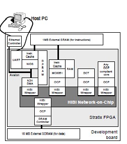
2. HIBI-based Multiprocessor SoC on FPGA by Erno Sal- minen, Ari Kulmala, and Timo D.Hamalainen, 2005
FPGAs offer excellent platform for System-on- Chips consisting of Intellectual Property (IP) blocks. The problem is that IP blocks and their interconnections is often FPGA vendor dependent. The HIBI Network-on-Chip (NoC) scheme solves the problem by providing flexible interconnection network and IP block integration with Open Core Protocol (OCP) interface. Therefore, IP compo- nents can be of any type: processors, hardware accelerators, communication interfaces, or memories. As a proof of con- cept, a multiprocessor system with eight soft processor cores and HIBI is prototyped on FPGA. The whole system
IJSER © 2011
http://www.ijser.org
International Journal of Scientific & Engineering Research Volume 2, Issue 12, December -2011 3
ISSN 2229-5518
uses 36402 logic elements, 2.9 Mbits of RAM, and operates on 78 MHz frequency on Altera Stratix 1S40, which is com- parable to other FPGA multiprocessors. The most impor- tant benefit is significant reduction of the design effort compared to system specific interconnection networks. HI- BI also presents the first OCP compliant IP-block integra- tion in FPGA.
3. Parallel Simulation of SystemC TLM 2.0 Compliant MPSoC on SMP Workstations byAline Mello, Isaac Maia, Alain Greiner, and Francois Pecheux June 2010.
The simulation speed is a key issue in virtual pro- totyping of Multi-Processors System on Chip (MPSoCs). The SystemCTLM2.0 (Transaction Level Modeling) ap- proach accelerates the simulation by using Interface Me- thod Calls (IMC) to implement the communications be- tween hardware components. Another source of speedup can be exploited by parallel simulation. Multi-core
workstations are becoming the mainstream, and SMP
workstations will soon contain several tens of cores. The
standard SystemC simulation engine uses a centralized scheduler that is clearly the bottleneck for a parallel simula- tion. This paper has two main contributions. The first is a general modeling strategy for shared memory MPSoCs, called TLM-DT (Transaction Level Modeling with Distri- buted Time). The second is a truly parallel simulation en- gine, called SystemC-SMP. First experimental results on a
40 processor MPSoC virtual prototype running on a dual- core workstation demonstrate.
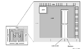
2.1 CLUSTER ARCHITECTURE
The proposed cluster-based MPSoC prototype
makes use of processing cores. These cores may be either
created or directly imported from any one of the core ven-
dors, available as a package along with the design suite
processor cores are integrated, four processing clusters and
a central node are created. This project consists of a hybrid
interconnected architecture, in which the NoC and hie-
rarchy bus based architecture were employed for inter- and
intra-clusters communication.
The Architecture of Cluster-based MPSoC
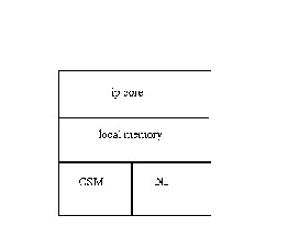
A single cluster
The processing cores are integrated to form a cluster and these clusters communicated with each other though a
IJSER © 2011
http://www.ijser.org
International Journal of Scientific & Engineering Research Volume 2, Issue 12, December -2011 4
ISSN 2229-5518
shared memory (CSM). Inside the clusters, each intellectual property core has its own local memory for executing the local tasks. It accesses the inter-cluster network by the shared network interface (NI).
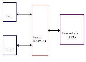
2.2 CENTRAL NODE
In this project work, the central node was a single-core SoC,
It is the one through which external peripherals can be ac-
cessed. The central node is the main control unit of the en-
tire architecture, which is responsible for scheduling the
parallel program. The computational data for various tasks
are collected and handed over to on different clusters. The
final output is also gathered by the central node gathering
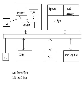
the executed results.
The Architecture of Processing Cluster
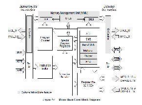
The processing cluster was based on Symmetric- Multiprocessor-like (SMP) architecture. For obtaining bet- ter performance of the cluster, hierarchial-bus based com- munication architecture was used. It means that communi- cation between the processing core and its local memory takes place through local bus. Communication with other cores is done using the shared memory on shared bus. The shared memory is divided into regions, in which one re- gion is dedicated for storing shared information, such as computational data for application, and other regions are used for exchanging data between clusters. The synchroni- zation between processor cores is achieved by semaphore register file, which could indicate the state of every region in shared memory and prevent core to modify the content when the region is locked. ie no other core can access the semaphore register except the core who has initially used it. The usage of resources from the shared memory as well as accessing the shared memory is done by round robin scheduling.
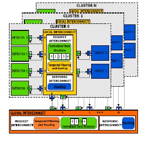
2.3 NETWORK CONNECTION
The Clusters and central node were interconnected
by an irregular network-on-chip, which was composed of 5
routers as the nodes of network. As shown in Fig.3, every
router has an identical network address, and connected by
physical link consisting of two channels of different trans-
ferring direction. In this NoC architecture, synchronized
handshake protocol was adopted as the flow control
scheme, and XY routing algorithm and Round-Robin arbi-
tration scheme was implemented too. The communication
within NoC was based on message passing among the dif-
ferent network nodes. In this design, the data packets of
transferring are organized in a standard format. Each pack-
et is rapid transmission, and each transmission contained
two bits for packets framing and 32 bits for data.
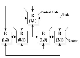
The Architecture of Interconnection Network
3. SYSTEM ON A CHIP
System-on-a-chip or system on chip (SoC or SOC) refers to integrating all components of a computer or other electronic system into a single integrated circuit (chip). It may contain digital, analog, mixed-signal, and often radio-frequency functions – all on a single chip sub- strate. A typical application is in the area of embedded sys- tems.
3.1 OVERVIEW OF SOC
Chip designs have for the last 20 years design ele-
ments. In an ASIC style flow, involving RTL logic synthesis
and automated standard cell place and route, the reuse ab-
straction has been at the basic cell level, where a cell
represents a few gates of complexity modules produced by
generators or by hand, such as memories etc. has been
common.
SoC design has involved the reuse of more com-
plex elements at higher levels of abstraction. Block-based
design, which involves partitioning, designing and assem-
bling SoCs using a hierarchical block-based approach, has
used the intellectual property (IP) block as the basic reusa-
ble element. This might be an interface function such as a
PCI or 1394 bus interface block; an MPEG2 or MP3 decod-
er; an implementation of data encryption or decryption
such as a Digital Encryption Standard (DES) block, or some
IJSER © 2011
http://www.ijser.org
International Journal of Scientific & Engineering Research Volume 2, Issue 12, December -2011 5
ISSN 2229-5518
complex function.
Recently, the platform-based design ap-
Design sign-in points in the design flow.
Efficient capturing of designer decisions.
proach to SoC designs has emerged. This approach arose in
consumer application such as wireless handsets and set-top
boxes. Elaborating on concepts presented in, we can define
a platform as a co-ordinated family of hardware-software
architectures, which satisfy a set of architectural con-
straints, imposed to allow the reuse of hardware and soft-
ware components. We call this a ―system platform‖. On a
more pragmatic basis, platform are collection of HW and SW IP blocks together with an on-chip communications architecture (on-chips buses, bridges, etc.) which usually include at least one processor, real-time operating system (RTOS), peripheral interface blocks, possible accelerating hardware blocks for specialized functions, middleware, and the option to customize the platform for specific appli- cations through drawing HW and SW IP blocks from libra- ries. Recent work in highly programmable platform, con- sisting of reconfigurable logic and fixed processor cores, has focused attention on embedded SW issues.
Essentially, there are only a limited number of fun-
damentally ―good‖ design solutions to the problems posed
by a particular application area. An application captures one or several related ―good‖ architectures, which are op- tional for an application domain, and allows their effective reuse in a low-risk manner with rapid time-to-market. From the base platform, a number of derivative SoC de- signs can be created rapidly and with far lower effort than with a block-based approach. Another fundamental ques- tion is one of economics: who pays for what in creating a platform and its design infrastructure-the semiconductor provider, the IP house (especially a processor IP house) or the system company? The future answer is quite unclear, although to date most investment has come from semicon- ductor and IP houses.
Notable industrial examples of platform include Philips with its Nexperia Digital Processing platform de- sign, Tality with Bluetooth designs, the BOPS voice-over-IP platform, the Metaflow Implosion SOC platform, Infineon M-Gold and TI OMAP wireless platforms, Parthus Medias- tream, Palmchip CoreFrame, and reconfigurable platforms from Lucent (Agere), Improv systems, Triscend, Altera Ex- calibur, Xilinx Vertex II, and Chameleon.
Areas of importance include:
Design Process
System design
Hardware Chip Design
Functional Verification
Analogous / Mixed-signal
Infrastructure
3.2 DESIGN PROCESS
This encompasses a set of basic processes to reduce
the risk of SoC design through the systematic collection
and reuse of design experience. The processes include:
Mechanisms for logging the design process, composing
Metrics for measuring the design and design progress.
Storage and retrieval of relevant design experience
Certification to ensure completeness of design process.
Qualification to ensure the sufficiency of design
decisions.
Process to use design experience for refining design
flow.
Such processes are important in order to increase confidence in taking a SoC design project; to ensure effec- tive reuse and minimal design time; to ensure that design experience is logged, and used for systematic improvement of SoC design processes and methods; and to allow quick assessment of the feasibility of a particular SoC design project. Further details on some of these processes can be found.
3.3 SYSTEM DESIGN
System-level design is fundamental to effective SoC de-
sign, and is particularly effective when married with plat-
form-based design concepts. The essential concept is to al-
low exploration of design derivatives at the system level of
abstraction, rather than the more traditional RTL and C
level. Functional-architecture co-design is a modern form
of design space exploration that goes beyond hardware-
software co-design, to permit a wider range of design tra-
deoffs. When platforms are modeled at the system level
with appropriate support for design space exploration, the
creation of a derivative design and its validation can be
done rapidly, with a high probability that the derivative
design implementation will be successful
3.4 HARDWARE CHIP DESIGN
In the SoC era, for both blocked-based and plat-
form-based methods, the emphasis is on chip integration,
not the individual customized design of each block. In the
platform-based approach, it is typical to design the ―hard-
ware kernel‖ or ―foundation block‖ of the platform as a
pre-laid-out, customized and characterized reusable ele- ment which forms part of every derivative design. The fixed hardware kernel generally incorporates the proces- sors, processor and system buses, memory interfaces, pos- sibly some fixed portion of memory, and bridges to peri- pheral bus. The platform-based design stage also usually fixes some part of the major SoC physical architectures: timing, test, power, etc. In the derivative design process for a platform-based design, the hardware kernal is assembled together with new, modified blocks from IP libraries to form the final hardware realization. .Of course, the blocks to be assembled need to be designed in the context of the overall SoC design plan and constraint.
The major steps required in hardware design include:
Chip planning
Block design-using RTL synthesis and automated place and route Analogous/mixed-signal block design Analogous/mixed-signal block design
IJSER © 2011
http://www.ijser.org
International Journal of Scientific & Engineering Research Volume 2, Issue 12, December -2011 6
ISSN 2229-5518
Memory block design
Processor core design and assembly
Bus design
Library verification
Chip assembly
The most important step is chip floor planning for both block-based and platform-based designs. The overall chip floor plan dictates the ease of block design and assembly, and imposes the major constraints on timing, power, test, etc. Development in hierarchical chip design tools offering advanced floor planning, es- timation and assembly capabilities for block-based ap- proaches are fundamental for SoC.
3.5 FUNDAMENTAL VERIFICATION
It has been repeatedly stated in recent years that
complex IC designs split into approximately 30-40% design
effort and 60-70% effort on verification. SoC design with its
additional system-level complexity only compounds this
problem. However a carefully chosen hierarchical verifica-
tion strategy involving modern tools can go a long way to
ameliorate this problem. The maze of current and new veri-
fication approaches, going beyond simple simulation, can
be overwhelming for users to understand. A good guide to
SoC functional verification is found in. Here it will suffice
to say that the emphasis in verification for SoC is a divide
and conquer strategy that exploits the underlying hierar-
chical nature of the SoC design; and a transaction-based
verification strategy that moves test bench stimulus, re-
sponse and checking up from the boolean signal level to
more complex data types and system level transaction.
When verification strategies map onto the underly-
ing SoC hierarchy, it is possible to verify designs block by
block using a unit test concept, and then using selectively
either the full block model, or a bus-functional model
equivalent, within the overall SoC verification model. Test
benches similarly can be built on a unit, block basis, and
reapplied within the overall SoC model. This is made much
easier if the test benches are architected to use the notion of
high level transactions that are ―natural‖ for the SoC. For
example, processor and peripheral blocks communicate within on-chip buses via various bus read/write and ac- quire /release transaction, and it is easier to create test benches that describe tests at this level and ―protocol- convert‖ them to bit-wise signal, than to write them all at the bit-wise level. In addition, this greatly facilities test bench reuse.
In the plat-form approach to SoC, reuse of test benches and verification models is a given, because the verification environment is first built for the platform, and then reused with little modification required for each derivative design. The only modifications needed are for any new IP blocks used, or for any blocks with modified functionality. Plat- form-based design allows the maximun amount of verifica- tion reuse when compared to a more custom, block-based SoC approach.
3.6 ANALOGUE / MIXED-SIGNAL
Although an increasing number of SoCs are mixed-
signal, the bulk of them today are still digital. i.e .big digital
small analog designs containing primary digital devices
with analog interfaces, the soc design approach is primarily
an integration approach. AMS blocks must be designed for
ease of integration onto a primarily digital device and chip
assembly process needs to encompass methods for easy
integration of these blocks.
3.7 INFRASTRUCTURE
Design information databases for IP blocks, plat-
forms and soc designs continue to evolve. Reuse of design
requires a well architectured and stable IP infrastructure in
which design blocks can be stored, searched for, found and
reliably retrieved. But the database infrastructure is only a
foundation or substructure. Of equal importance are a set
of ip management process and procedures that allow effec-
tive use of the underlying database capabilities. Here effec-
tive characterization and rapid search for IP blocks and
platforms is a key requirement.
4. NETWORK ON CHIP
Network-on-Chip or Network-on-a-Chip (NoC) is
an approach to designing the communication subsystem
between IP cores in a System-on-a-Chip (SoC). NoCs can
span synchronous and asynchronous clock domains or use
unclocked asynchronous logic. NoC applies networking
theory and methods to on-chip communication and brings
notable improvements over conventional bus and crossbar
interconnections. NoC improves the scalability of SoCs,
and the power efficiency of complex SoCs compared to
other designs.
4.1 Why NOC?
• Efficient sharing of wires
• Lower area / lower power / faster operation
• Shorter design time, lower design effort
• Scalability
• Enable using custom circuits for communication
4.2 NOC FLOW
• Basic unit exchanged by end-points is the PACKET
• Packets broken into many FLITs
– ―flow control unit‖
– Typically # bits = # wires in each link (variations)
– Typically contains some ID bits, needed by each
switch along the path:
• Head / body / tail
• VC #
• SL #
• FLITs typically sent in a sequence, making a ―worm‖ go- ing through wormhole.
• Unlike live worms, FLITs of different packets may inter- leave on same link
IJSER © 2011
http://www.ijser.org
International Journal of Scientific & Engineering Research Volume 2, Issue 12, December -2011 7
ISSN 2229-5518
4.3 NOC ARCHITECTURE
Several architectures have been proposed in the
NoC literature. However, all NoCs have three fundamental
building blocks, namely, switches (also called routers),
Network Interfaces (NIs) (also called network adapters)
and links. The NoC is instantiated by deploying a set of
these components to form a topology and by configuring
them in terms of buffer depth, etc. The backbone of the
NoC consists of switches, whose main function is to route
packets from sources to destinations. Some NoCs rely on
specific topological connectivity, such as octagon or ring, to
simplify the control logic, while others allow for arbitrary
connectivity, providing more flexible matching to the tar-
get application. NoCs can be based on circuit or packet
switching, or a mix of both; the former is aimed at provid-
ing hard QoS guarantees, while the latter optimizes the
efficiency for the average case. When packet switching is
chosen, switches provide buffering resources to lower con-
gestion and improve performance. They also handle flow
control issues, and resolve conflicts among packets when
they overlap in requesting access to the same physical
links. Two of the most usual flow control protocols involve
switch-to-switch communication and are retransmission
based (i.e., packets are optimistically sent but a copy of
them is also stored by the sender, and, if the receiver is
busy, a feedback wire to request retransmission is raised)
or credit-based (i.e., the receiver constantly informs the
sender about its ability to accept data, and data are only
sent when resources are certainly available). End-to-end
flow control schemes, where peripheral NIs directly ex-
change flow control information with each other, are more
rarely used because of their buffering requirements; the
most common usage scenario involves NoCs that imple-
ment circuit switching.
An NI is needed to connect each core to the NoC. NIs converts transaction requests/responses into packets and vice versa. Packets are then split into a sequence of
FLow control unITS (FLITS) before transmission, to de- crease the physical wire parallelism requirements. NIs is associated in NoCs to system masters and system slaves. Many current NoC solutions leverage static source routing, which means that dedicated NI Look-Up Tables (LUTs) specify the path that packets will follow in the network to reach their final destination. This type of routing minimizes the complexity of the routing logic in the NoC. As an alter- native, routing can be performed within the topology itself, normally in an adaptive manner; however, performance advantages, in-order delivery and deadlock / livelock freedom are still issues to be studied in the latter case.
In general, two different clock signals can be at- tached to NIs: the first one drives the NI front-end, the side to which the external core is attached, and the second one drives the NI back-end, the internal NoC side. These clocks can, in general, be independent. This arrangement enables the NoC to run at a different (and potentially faster) clock than the attached cores, which is crucial to keep transaction latency low. In this work we employ the _pipes NoC li- brary, as a state-of-the-art NoC solution that incorporates most of the features and effective architectural solutions that have been proposed in NoC designs; thus, it is repre- sentative of various reasonable design points. The _pipes NoC is an example of a highly flexible library of compo- nent blocks.
The NoC can employ any of ACK / NACK (re- transmission-based) or STALL / GO (credit based) flow control protocols, using output or input buffering, respec- tively, for maximum efficiency. Links can be pipelined and no virtual channels are implemented, as this allows for a much leaner implementation. Deadlocks are avoided by construction in the definition of the routing tables included in the NIs. Two separate NIs are defined, i.e., an initiator one (for the master cores) and a target one (for the slave cores); a master/slave device requires an NI of each type to be attached to it. The interface among cores and NIs is point-to-point as defined by the Open Core Protocol (OCP)
2.0 specification used as public interface of the NoC, guar- anteeing maximum reusability for different cores and MPSoCs. _pipes NIs support two different clock signals, one for the OCP interface and another one for the _pipes internal interface; the _pipes clock frequency must be an integer multiple of the OCP one, to greatly simplify the hardware and performance overhead of clock synchroniza- tion. Since each core can run at a different divider of the
_pipes frequency, mixed-clock platforms are possible,
which provides large flexibility.
4.3.1 NOC Level
• Circuits
– Wires, Buffers, Routers, NI
• Network
– Topology, routing, flow-control.
• Architecture
– Everything is packets.
– Traffic must be characterized.
– NoC can extend to other chips.
IJSER © 2011
http://www.ijser.org
International Journal of Scientific & Engineering Research Volume 2, Issue 12, December -2011 8
ISSN 2229-5518
• Support known traffic patterns
– CPUs to Shared Cache.
– Cache to external memory.
– Special I/O traffic: Graphic, wireless / wired
communication.
• Support unexpected traffic patterns
• Provide new services
– Provide cache coherency.
– Manage the shared cache.
– Schedule tasks / processes / threads.
– Support OS.
– Support other memory models.
NOC ARCHITECTURE
5. IMPLEMENTATION
The whole project is implemented in a reconfigur- able hardware structure like FPGA and a softcore micro- controller such as microblaze.
5.1 FPGA
A Field-Programmable Gate Array (FPGA) is an in-
tegrated circuit designed to be configured by the customer
or designer after manufacturing—hence "field-
programmable". The FPGA configuration is generally
specified using a hardware description language (HDL),
similar to that used for an application-specific integrated
circuit (ASIC) (circuit diagrams were previously used to
specify the configuration, as they were for ASICs, but this
is increasingly rare). FPGAs can be used to implement any
logical function that an ASIC could perform.
FPGAs contain programmable logic components
called "logic blocks", and a hierarchy of reconfigurable in-
terconnects that allow the blocks to be "wired together"—
somewhat like a one-chip programmable breadboard.
Logic blocks can be configured to perform complex combi-
national functions, or merely simple logic gates like AND
and XOR. In most FPGAs, the logic blocks also include
memory elements, which may be simple flip-flops or more complete blocks of memory.
In addition to digital functions, some FPGAs have analog features. The most common analog feature is pro- grammable slew rate and drive strength on each output pin, allowing the engineer to set slow rates on lightly loaded pins that would otherwise ring unacceptably, and to set stronger, faster rates on heavily loaded pins on high- speed channels that would otherwise run too slow. An- other relatively common analog feature is differential com- parators on input pins designed to be connected to differ- ential signaling channels. A few "mixed signal FPGAs" have integrated peripheral Analog-to-Digital Converters (ADCs) and Digital-to-Analog Converters (DACs) with analog signal conditioning blocks allowing them to operate as a system-on-a-chip. Such devices blur the line between an FPGA, which carries digital ones and zeros on its inter- nal programmable interconnect fabric, and field- programmable analog array (FPAA), which carries analog values on its internal programmable interconnect fabric.
The FPGA used for this project is Spartan 3E. The Spartan-3E family architecture consists of five fundamental programmable functional elements:
• Configurable Logic Blocks (CLBs) contain flexible Look- Up Tables (LUTs) that implement logic plus storage ele- ments used as flip-flops or latches. CLBs perform a wide variety of logical functions as well as store data.
• Input/Output Blocks (IOBs) control the flow of data be- tween the I/O pins and the internal logic of the device. Each IOB supports bidirectional data flow plus 3-state op- eration. It supports a variety of signal standards, including four high-performance differential standards. Double Data- Rate (DDR) registers are included.
• Block RAM provides data storage in the form of 18-Kbit dual-port blocks.
• Multiplier Blocks accept two 18-bit binary numbers as inputs and calculate the product.
• Digital Clock Manager (DCM) Blocks provide self- calibrating, fully digital solutions for distributing, delaying, multiplying, dividing, and phase-shifting clock signals.
SPARTAN 3E ARCHITECTURE
IJSER © 2011
http://www.ijser.org
International Journal of Scientific & Engineering Research Volume 2, Issue 12, December -2011 9
ISSN 2229-5518
5.2 MICROBLAZE
The MicroBlaze™ embedded processor soft core is a reduced instruction set computer (RISC) optimized for implementation in Xilinx® Field Programmable Gate Ar- rays (FPGAs). The MicroBlaze soft core processor is highly configurable, allowing you to select a specific set of fea- tures required by your design.
In addition to these fixed features, the MicroBlaze
processor is parameterized to allow selective enabling of additional functionality. Older (deprecated) versions of MicroBlaze support a subset of the optional features de- scribed in this manual. Only the latest (preferred) version of MicroBlaze (v7.10) supports all options.
Thirty-two 32-bit general purpose registers, 32-bit
instruction word with three operands and two addressing modes, 32-bit address bus.
CONCLUSION
The cluster based multiprocessor system on chip
architecture can be designed using cores provided by the
microblaze controller and spartan 3E kit. Some of the cores
that are used are UART, FFT, FIR, Encoder, Multiplier, I2C
CORE etc.
The basic building block of this MPSOC design me-
thodology is the configurable, extensible microprocessor
core, created by a processor generator that uses high-level
specifications of application-domain requirements in the
form of instruction-set descriptions or even examples of the
application code to run to generate small, efficient, applica-
tion-specific, programmable microprocessors. Configurable
processors can perform traditional microprocessor tasks
quite efficiently. But because these configurable processors
are able to incorporate the data paths, instructions, and
register storage for an application’s own natural data types,
they also support virtually all of the functions that chip designers have historically implemented as hard-wired logic. The introduction of configurable, extensible proces- sors changes the SOC design equation. These processors can now deliver very high performance. The performance
per gate, per square millimeter of silicon, per watt, or per clock delivered by these processors often rivals or exceeds the performance of hard-wired logic blocks that they re- place.
REFERENCES
1. A formal approach to MpSoC performance verification
by Richter, K.; Jersak, M.; Ernst, R.
2. Dynamic Task Mapping for MPSoCs by Ewerson Luiz de
Souza Carvalho,
3. www.xilinx.com
4. www.altera.com
5. www.arm.com
6. Multilevel MPSoC Performance Evaluation Using MDE
Approach by Rabie Ben Atitallah, Lossan Bonde, Smail
Niar, Samy Meftali, Jean-Luc Dekeyser
7. L. Benini et al., ―MPARM: Exploring the Multi-Processor
SoC Design Space with SystemC,‖ Springer J. of VLSI Sig-
nal Processing, 2005.
IJSER © 2011
http://www.ijser.org