International Journal of Scientific & Engineering Research, Volume 4, Issue 4, April-2013 664
ISSN 2229-5518
![]()
Abstract- This paper deals with the low power methods available for the testing of VLSI Systems. The problems faced have been analyzed and the solutions available are discussed. Since extra power consumption can result in severe hazards, it becomes vital that methods which are power efficient and also safe are devised. The lower power testing methods allow non- destructive testing of VLSI system.
Index Terms: BIST, energy and power modeling, low power testing ,external Testing, ATPG, ordering techniques, reduced power consumption .
—————————— ——————————
With the recent advancements in technology and its continuous up-gradation, there has been an explosion in both the size and the intricacies of complex digital circuits. Miniaturization has brought about this change and with improvements in the Silicon manufacturing technology, these improvements will continue in the future too. However, this complicates the testing of these designs. The test phase is indispensible as it is the only way to find innovative solutions and hence is the most expensive part of any design cycle.![]()
Power consumption consideration is important as any system consumes more power in test mode than in system mode. This is because successive test patterns do not have any similarity and hence involve huge switching activity in test mode, compared to system mode [3].Since power dissipation is proportional to the amount of switching activity, too much of switching activity during test might lead to several problems, including performance deterioration and battery life reduction. The following three parameters determine the power properties of a system being put to test:
Debasmita Hazra is pursuing final year of Electronics & Communication Engineeering at Vellore Institute of Technology, Vellore, India, E-mail:dhazra91@gmail.com
Switching activity involved in test mode as energy consumed is directly proportional to it.
Average power consumption which is nothing but the ratio between the energy consumed and the test length.
Peak power consumption corresponding to highest energy consumed in one clock period divided by total test length, or the highest switching activity in one clock period. Since peak power determines the thermal and electrical limitations, it must be limited within a certain range or else the functioning of the circuit can be hampered.
Embedding the tester equipment functionality into the semiconductor product reduces both the burden on and the complexity of external test equipment, and makes the on-chip access simplistic and faster. BIST is extra circuitry to enable complete testing without much external help[1]. It basically consists of a test pattern generator, test response compactor, test response comparator, and control circuitry to carry out the test process and give the GO/NOGO signal.
IJSER © 2013
International Journal of Scientific & Engineering Research, Volume 4, Issue 4, April-2013 665
ISSN 2229-5518
LFSR (Linear Feedback Shift Register): Produces pseudorandom input vectors, and hence called a PRPG (Pseudo Random Pattern Generator)
MISR (Multiple Input Signature Register):
Another type of LFSR that compresses the response of the CUT(Circuit Under Test) into a signature to be compared to a good circuit’s response.
Control circuitry.
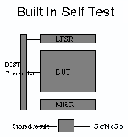
Fig1:BIST Module
The BIST results, "pass" or "fail", depend on whether the signature captured into the MISR matches the one coming out of the good circuit.
Non- destructive testing, cost, reliability, performance verification, autonomy as well as technology related issues, motivating for power consumption minimization during test application are the factors to be considered while choosing a test method.
Increased maximum current flow is caused due to excessive switching activity during the test. This calls for the need for a more expensive packaging of consumer electronic products. In case conductors get eroded due to electro-migration whose rate is influenced by temperature and current density, circuit failure may occur. Hence reliability of circuit reduces when switching rate is high as that increases the temperature and also current. As BIST circuits may be tested too often, electro-migration is even more severe. As remote systems are mostly operated in
stand-by mode, power saving during test mode can prolong the battery life.
The functional testing and normal operation modes differ in the power dissipation. As just after wafer etching, the packaging is not done, power dissipation is negligible while during normal operation, packaging is done taking power dissipation into account. Hence, heat removal techniques cannot be implemented during bare die testing. This poses a problem in applications based on MCMs.
Another reason for power minimization to be adopted is problems are encountered while testing memories via wafer probes[2]. During wafer probing, switching activity is high and hence power dissipation and ground noise are serious. The excessive noise can erroneously change the logic state of circuit lines, causing some good dies to fail the test, thus leading to unnecessary loss of yield.
External testing has become more difficult due to the modern design and package technologies. BIST is a testing methodology in which faulty components can be detected, by incorporating test logic on-chip[1]. Hence it is a comparatively promising external testing technique. This method is advantageous as provides improved testability, at clock- speed testing of modules, reduced need for automatic test equipment , and support during system maintenance. This method also preserves the intellectual property of the system. The test patterns in this method are generated using Linear Feedback Shift Register (LFSR). But the use of LFSR increases the energy consumption as the test length has to be increased to achieve larger coverage. The autonomy of portable equipment hence decreases. Special packaging is also required in this case which increases the final product cost. In order to satisfy the cost, performance verification, autonomy and reliability constraints, it is therefore very important to reduce the power/energy dissipation during testing.
In scan- based BIST, the architecture is really expensive[1]. This is due to the fact that each test pattern is accompanied by a shift pattern with high power consumption to provide test patterns and evaluate the test responses. In industrial environment this is a phenomenon highly observed. So to reduce the danger of system destruction and meet the
IJSER © 2013 http://www.ijser.org
International Journal of Scientific & Engineering Research, Volume 4, Issue 4, April-2013 666
ISSN 2229-5518
specified power limits, the power consumption during scan shifting should be reduced.
CMOS circuits witness the following kind of power dissipation:
Static power dissipation resulting from leakage current or due to other current being drawn continuously from the power supply.
Dynamic power dissipation due to short
circuit current and charging and discharging of load capacitance during output switching. It dominates over static power disspation in CMOS.
The average energy consumed at node i per switching can be represented as (1/2CiV2DD) where Ci is the equivalent output capacitance and VDD the power supply voltage. Therefore for si number of switchings during the period, the energy consumed (1/2Ci si V2DD).Nodes connected to multiple gates display higher parasitic capactitance.Hence it can be assumed that Ci is proportional to the fan-out of the node Fi. Therefore,the energy Ei consumed at node i during one clock period is
Ei= (1/2si FicoV 2DD ),
where co is the minimum parasitic capacitance corresponding to the minimum size on the circuit. This energy estimate is proportional to the calculation of fan out Fi and the number of switchings on node i, s, which can be determined by the circuit topology and a logic simulator respectively. The product(Fi*si) is the Weighted Switching Activity(WSA) of node i and represents the only variable part in the energy consumed at node i during test application. Hence ,if now all the nodes and all the switching activity involved is included in the formulation for a total test length of
T, then the total energy consumed during the entire test application is:
Etotal=(1/2si FicoV 2DD ∑k∑is(i,k)).
The instantaneous power is the power consumed in one clock period and is given by Pinst(Vk)=EVk/T.
Peak power consumption is the maximum instantaneous power consumed during the test session and is expressed by
Ppeak=maxk Pinst (Vk)= maxk (EVk )/T.
Finally,the average power consumed in the total test time is the total energy divided by the total test length and is given by:
Pave= Etotal/T.
Thus the following can be observed from the above:
For a given supply voltage and CMOS technology, the number of switchings involved,creates an impact on the energy,peak power and average power consumption.
It is the clock frequency used in testing, that determines the peak power and average power.
Finally the test duration,and the number of test patterns employed commands the total energy consumption.
In order to ensure non-destructive testing of a circuit, such testing should be adopted that the circuit switching resembles the one during normal circuit operation. Many categories of techniques have been developed for this purpose as discussed below.
IJSER © 2013 http://www.ijser.org
International Journal of Scientific & Engineering Research, Volume 4, Issue 4, April-2013 667
ISSN 2229-5518
These techniques aim at generating test patterns which reduce the power dissipated during test application. Under this in the PODEM algorithm, the new version proposes the assignment of don’t care bits to minimize the number if transitions occurring between two consecutive test vectors. It reduces average and peak power dissipation during test application. This method is adopted for full scan sequential circuits.
Another proposed ATPG technique exploits the redundancy introduced in test pattern generation phase. A subset of sequences such that power consumed reduces without reducing the fault coverage is selected.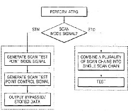
Fig 2:ATPG Operation
In this category such techniques are included which reduce the switching activity by altering the order in which the test vectors of the test sequence are applied to the CUT. These can be used in both external testing and also in deterministic BIST.
In the circuits designed with a scan path structure, the power dissipation during test operation can be reduced by modifying the order in which scan flip flops are arranged to form the shift register.
Another technique that maybe used is such that the CUTS inputs remain unaltered while the scan path structure is altered.
Power consumption during Built -in Self-Test can be reduced in several ways:
Firstly, the execution of every BIST element can be scheduled such that the power dissipation is kept under the specified limits. The average power is reduced and the temperature related problems can be avoided by expanding the test length. Simultaneously, the total energy remains constant.
Secondly, the read/write access and the address counting scheme can be reordered such that there is a reduction in the RAM transitions. It not only decreases he energy consumption but also the power since the test time is preserved.
Thirdly, there is a method to reduce the average power and energy consumption by about 13% to
70 % by employing two different speed LFSRs,
where inputs with elevated transition density are connected to the low speed LFSR.
Fourthly, the scan cells can be path structure modified such that the CUT input remain unchanged during shift operation. About 70% to
90% energy savings can be witnessed.
Fifthly, a novel idea is to partition the circuit into two parts such that each sub-circuit can be successively tested through two different BIST sessions[5]. This reduces the switching activity in a time interval and the peak power consumption. Since the total test length required to test the two sub-circuits is almost same as the test length of the original circuit, the energy consumption during BIST is also reduced.
IJSER © 2013 http://www.ijser.org
International Journal of Scientific & Engineering Research, Volume 4, Issue 4, April-2013 668
ISSN 2229-5518
Research is being carried out to a great extent to develop low power methods for the testing of VLSI systems. In this paper, the problems caused due to the power dissipation external testing and BIST techniques have been described. Then the latest techniques available to reduce power and/or energy consumption have been discussed.
[1]S. Gerstendiirfer and H.J. Wunderlich, “Minimized Power Consumption for Scan-based BIST “, to appear in the proceedings of IEEE Int. Test Conf., September 1999.
[2] J. Monzel, S. Chakravarty, V.D. Agrawal, R. Aitken, J. Braden, J. Figueras, S. Kumar, H.-J. Wunderlich and Y. Zorian,“Power Dissipation During Testing : Should We Worry About it ?“, Panel Session, IEEE VLSI Test Symp., Monterey, USA,April 1997.
[3] R. Parkar, “Bare Die Test “, IEEE Multi-Chip Module
Conf., pp. 24-27, 1992.
[4] P. Girard, L. Guiller, C. Landrault and S. Pravossoudovitch, “Circuit Partitioning for Low Power BIST Design with Minimized Peak Power Consumption”, to be presented at IEEE Asian Test Symp., November
1999.
IJSER © 2013 http://www.ijser.org