The research paper published by IJSER journal is about A Novel Design and Simulation of 2 Digit BCD Adders Using Reversible Gates 1
ISSN 2229-5518
A Novel Design and Simulation of 2 Digit BCD Adders Using Reversible Gates Ankur Saxena, Mohd. Tauheed Khan
AFSET, Maharishi Dayanand University, India
ank.saxena@gmail.com, khantauheed@gmail.com
Abstract- Reversible quantum computer is gaining interest for the future computer system. With the advent of quantum computer and reversible logic, design and implementation of all devices has received more attention. BCD digit adder is the basic unit of the more precise decimal computer arithmetic. The research objective is to increase speed of operation for addition of BCD numbers while minimizing the power dissipation by using reversible gates. This paper proposes one new reversible logic gate MAS. The MAS gate can be used as full adder and also reduces the number of garbage outputs. It can also be used as “Copying Circuit” to increase fan-out because fan-out is not allowed in reversible circuits. This paper also proposes a novel reversible design of 2 digit BCD full adder. The simulation result of 2 digit BCD adder on ModelSim are also included.
Keywords- BCD Adder, Design, Full Adder, Reversible Gate, Reversible Logic, Quantum Computing, Simulation.
I. INTRODUCTION
The information loss in irreversible logic results in energy dissipation. According to Landauer’s principle, the loss of one bit of information dissipates kTln2 joules of energy where k is the Boltzmann’s constant and T is the absolute temperature at which the operation is performed [6] Later Bennett, in 1973, showed that in order to avoid kTln2 joules of energy dissipation in a circuit it must be built from reversible circuits. Reversible logic supports the process of running the system both forward and backward. This means that reversible computations can generate inputs from outputs and can stop and go back to any point in the computation history. Thus, reversible logic circuits offer an alternative that allows computation with arbitrarily small energy dissipation. Furthermore, reversible circuits are of major interest in optical computing, low power design & quantum computing. It is not possible to realize quantum computing without reversible logic. Reversible computation in a system can be performed if the system is composed of reversible gates [15].
A circuit (gate) is reversible if there is a one-to-one correspondence between the inputs and the outputs. Thus, any reversible gate has the same number of input and output lines, and it implements a permutation from input values to output values. Neither feedback nor fanout is allowed in reversible logic [8]. Consequently, synthesis of reversible logic is different from irreversible logic synthesis. One of the major constraints in reversible logic is to minimize the number of reversible gates used and garbage outputs produced. Garbage output refers to the output that is not used for further
computations [12]. A logic synthesis technique using reversible gate should have the following features [9]:
1. Produce minimum number of garbage outputs
2. Use minimum input constants
3. Keep the length of cascading gates minimum
4. Logic implemented with minimum number of gates
In this research, one new reversible logic gate is introduced. Further, this paper introduces a novel reversible 2 digit BCD adder using the proposed MAS gate with minimal number of reversible gates and garbage outputs.
II. MATERIALS AND METHODS
Reversible Logic Gates: There is a number of existing reversible logic gates such as Feynman Gate, FG[2], Toffoli Gate, TG[14],Fredkin Gate, FRG, New Gate, NG [1],and New Toffoli Gate, NTG [11] [5].
A 2*2 Feynman Gate, also known as controlled NOT (1- CNOT). It implements the logic functions: P=B and
Q=A⊕B. Feynman Gate is the most suitable gate for a
single copy of a bit. A „0‟ in the second input will copy
the first input in both outputs of the gate. Thus, Feynman Gate is the most suitable gate for single copy of bit since it is not producing any garbage output.
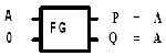
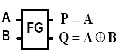
Fig 1: Feynman Gate Fig 2: Feynman Gate as copying gate
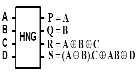
A generalized, k-way, Toffoli Gate has k + 1 inputs: k control inputs, that are copied to the first k outputs, and one other input that is complemented if all control inputs are 1s and is directly copied to the last output otherwise. A 3-input, 3-output Toffoli Gate is shown in Fig. 3. The inputs „A‟ and „B‟ are passed as first and second output respectively. The third output is controlled by „A‟ and „B‟ to invert „C‟.
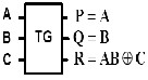
Fig 3: Toffoli Gate Fig 4: HNG Gate
IJSER © 2012 http://www.ijser.org
The research paper published by IJSER journal is about A Novel Design and Simulation of 2 Digit BCD Adders Using Reversible Gates 2
ISSN 2229-5518
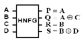
Fig 5: HNFG Gate
Gate width of HNFG and HNG is 4 [7].In the other
words, HNFG and HNG are 4-input, 4-output reversible gates. Furthermore, both of them are two-through gates, which mean that two input variables are also outputs. Each HNFG gate can be used as two well-known 2*2
Table 1:
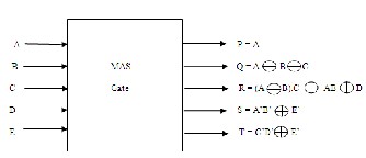
Fig 7: The Proposed MAS Gate
Feynman gates. It also can be used as “Copying Circuit” to increase fan-out because fan-out is not allowed in reversible circuits.
Reversible 4 bit parallel adder: A BCD adder circuit adds two BCD numbers and converts the result into its equivalent BCD number. The conversion is needed because of the occurrence of overflow of the addition.
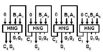
Fig 6: 4-Bit Ripple Carry Adder using reversible HNG gates
We use the reversible full adder depicted in Fig.4 to construct a reversible 4-bit parallel adder shown in Fig.
7.
The Proposed MAS Gate: The width of proposed MAS
gate is 5 i.e. it has 5-input, 5-output reversible gates.
The MAS gate is used to generate the correction logic. The sum bits and carry bit, if any, from first stage ripple carry adder are checked and if incorrect BCD sum is generated or carry bit is generated with correct BCD sum bits, MAS gate generates correction logic „6‟ which is added to second stage 4-bit ripple carry adder.
Truth Table of proposed reversible MAS Gate
IJSER © 2012 http://www.ijser.org
The research paper published by IJSER journal is about A Novel Design and Simulation of 2 Digit BCD Adders Using Reversible Gates 3
ISSN 2229-5518
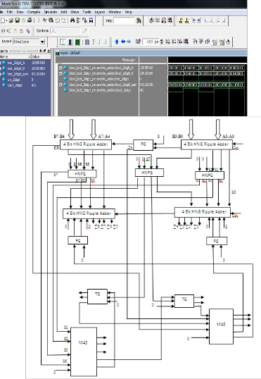
Fig 8: Proposed 2 Digit Reversible BCD Adder
III. DESIGN SIMULATION
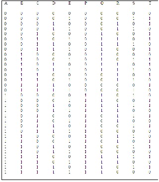
Fig 9: Simulation Results of 2 Digit BCD Adder
The simulation results shown in figure 9 are obtained by simulating an RTL design of 2 digit BCD adder developed using the proposed 1 digit BCD adder design [15] .
IV. RESULTS AND DISCUSSION
In this paper, we proposed one novel 5*5 reversible logic gate called MAS gate. We have designed a new reversible full-adder circuit that requires only one reversible MAS gate and produces zero garbage outputs. The design would increase the performance of quantum computing since the proposed design is capable of adding 2 digits of BCD numbers simultaneously. Table 2 shows the results of new proposed design.
Table 2:
Analysis of 2 digit BCD adder
| No of Gates | No of Garbage Outputs |
This work | 25 | 42 |
V. CONCLUSION
The design of 2 digit BCD adder is proposed. BCD adder is necessary requirement of quantum computers, because quantum computers must be built from reversible components. The proposed BCD adder poses all the good features of reversible logic synthesis.
REFERENCES
[1] Azad Khan Md. M. H., Design of full adder with reversible gate.
International Conference on Computer and Information Technology, Dhaka, Bangladesh, pp. 515-519, 2002.
[2] Feynman R., . Quantum mechanical computers. Optics News, 11: 11 -
20. 1985.
[3] Hasan Babu Hafiz Md. and Ahsan Raja Chowdhury, . Design of a reversible binary coded decimal adder by using reversible 4-bit parallel
adder. VLSI Design 2005, Kolkata, India, pp. 255 -260, 2005.
[4] Hasan Babu Hafiz Md., Md. Rafiqul Islam, Ahsan Raja Chowdhury and Syed Mostahed Ali Chowdhury, On the realization of reversible
full adder circuit. International Conference on Computer and
Information Technology, Dhaka,Bangladesh, 2: 880-883, 2003
[5] Hasan Babu Hafiz Md., Md. Rafiqul Islam, Syed Mostahed Ali
Chowdhury and Ahsan Raja Chowdhury, Reversible logic synthesis for minimization of full adder circuit. Proceeding of the EuroMicro Symposium on [6] Digital System Design (DSD 03), Belek Antalya, Turkey, pp. 50-54, 2003.
[6] Landauer R., Irreversibility and heat generation in the computing process. IBM J.Research and Development, 5(3): 183-191, 1961.
[7] Majid Haghparast and Keivan Navi, Science Publications, A Novel Reversible BCD Adder For Nanotechnology Based systems, American Journal of Applied Sciences 5 (3): 282-288, 2008,ISSN 1546-9239,
2008.
[8] Parhami B., Fault tolerant reversible circuits.Proc. 40th Asilomar Conf.
Signals, Systems, and Computers, October 2006, Pacific Grove, CA,
2006.
[9] Perkowski M., A. Al-Rabadi, P. Kerntopf, A. Buller, M. Chrzanowska - Jeske, A. Mishchenko, M.Azad Khan, A. Coppola, S. Yanushkevich,
V.Shmerko and L. Jozwiak, A general decomposition for reversible logic, Proc. RM 2001,Starkville, pp. 119 -138, 2001.
[10] Perkowski M and P Kerntopf, Reversible Logic. Invited tutorial, Proc.
EURO-MICRO, Sept 2001, Warsaw, Poland, 2001.
[11] Peres A., Reversible logic and quantum computers. Physical Review.
A 32: 3266-3276, 1985.
IJSER © 2012 http://www.ijser.org
The research paper published by IJSER journal is about A Novel Design and Simulation of 2 Digit BCD Adders Using Reversible Gates 4
ISSN 2229-5518
[12] Thapliyal Himanshu and M. B. Srinivas, Novel reversible TSG gate and its application for designing reversible carry look ahead adder and other adder architectures. Proceedings of the 10th Asia-Pacific Computer Systems Architecture Conference (ACSAC 05), Lecture Notes of Computer Science, 3740: 775-786. Springer-Verlag, 2005.
[13] Thapliyal H., S. Kotiyal, M. B. Srinivas, Novel BCD adders and their
reversible logic implementation for IEEE 754r format. Proceedings of the 19th International Conference on VLSI Design, 3 -7 Jan 2006,
2006.
[14] Toffoli T.,Reversible computing. Tech Memo MIT/LCS/TM-151, MIT Lab for Computer Science, 1980.
[15] Vasudevan D. P., P. K. Lala and J. P. Parkerson, Online testable
reversible logic circuit design using NAND blocks. Proc. Symposium on Defect and Fault Tolerance, pp. 324-331, 2004.
[16] Palnitkar, Sami, Verilog HDL: A Guide to Digital Design & Synthesis.
Sunsoft press. 1996.
IJSER © 2012 http://www.ijser.org