International Journal of Scientific & Engineering Research Volume 2, Issue 10, Oct-2011 1
ISSN 2229-5518
A Fuzzy logic DC-Link Voltage Controller for Three-Phase DSTATCOM to Compensate AC and DC Loads
Kranthi Kumar Kora
—————————— ——————————
The proliferation of power-electronics- based equipment, nonlinear and unbalanced loads, has aggravated the power-quality (PQ) problems in the power distribution network. They cause excessive neutral currents, overheating of electrical apparatus, poor power
power electronics engineering in sri vasavi engineering college in Jawaharlal Nehru technological University, India, PH-08818-284355. E-mail: kranthikumar.kora@gmail.com
Based on this algorithm, the compensator reference
∗ ,i ∗ i ∗ ) are given as fallows.
factor, voltage distortion, high levels of neutral-to-ground
currents (ifa
fb, fc
![]()
v
+ y(v
− v )
voltage, and interference with communication systems [1],
[2]. The literature records the evolution of different custom
i ∗ = ila −
sa sb
![]()
∑i=a b c v 2
sc
( lavg
+ pdc )
, , si
power devices to mitigate the above power-quality
problems by injecting voltages/currents or both into the system [3]–[6].
The shunt-connected custom power device, called
∗
fb lb
∗
fc lc
vsb + y(vsc − vsa )
![]()
∑i=a b c v 2
vsc + y(vsa − vsb )
∑i=a b c v 2
(plavg + pdc )
(plavg + pdc )
the distribution static compensator (DSTATCOM), injects
current at the point of common coupling (PCC) so that harmonic filtering, power factor correction, and load balancing can be achieved. The DSTATCOM consists of a current-controlled voltage-source inverter (VSI) which injects current at the PCC through the interface inductor. The operation of VSI is supported by a dc storage capacitor with proper dc voltage across it.
One important aspect of the compensation is the extraction of reference currents. Various control algorithms are available in literature [7]–[11] to compute the reference compensator currents. However, due to the simplicity in formulation and no confusion regarding the definition of powers, the control algorithm based on instantaneous symmetrical component theory [11] is preferred.
————————————————
Kranthi Kumar Kora is currently pursuing masters degree program in
Where y = tan∅/√3, ∅ is the desired phase angle between
the supply voltages and compensated source currents in the
respective phases. For unity power factor operation, ∅ = 0, thus y = 0. The term plavg is the dc or average value of the load power. The term pdc in (1) accounts for the losses in the VSI without any dc loads in its dc link. To generate pdc , a
suitable closed-loop dc-link voltage controller should be
used, which will regulate the dc voltage to the reference value.
For the DSTATCOM compensating unbalanced
and nonlinear loads, the transient performance of the compensator is decided by the computation time of average load power and losses in the compensator. In most DSTATCOM applications, losses in the VSI are a fraction of the average load power. Therefore, the transient performance of the compensator mostly depends on the
computation of plavg . In this paper,plavg is computed by
IJSER © 2011 http://www.ijser.org
International Journal of Scientific & Engineering Research Volume 2, Issue 10, Oct-2011 2
ISSN 2229-5518
using a moving average filter (MAF) to ensure fast dynamic response. The settling time of the MAF is a half-cycle period in case of odd harmonics and one cycle period in case of even harmonics presence in voltages and currents.
Although the computation of pdc is generally slow and
updated once or twice in a cycle, being a small value
compared to plavg , it does not play a significant role in
transient performance of the compensator.
In some of the electric power consumers, such as the telecommunications industry, power-electronics drive applications, etc., there is a requirement for ac as well as dc loads [12]–[15]. The telecommunication industry uses several parallel-connected switch-mode rectifiers to support dc bus voltage. Such an arrangement draws nonlinear load currents from the utility. This causes poor power factor and, hence, more losses and less
efficiency. Clearly, there are PQ issues, such as unbalance,
poor power factor, and harmonics produced by telecom equipment in power distribution networks. Therefore, the functionalities of the conventional DSTATCOM should be increased to mitigate the aforementioned PQ problems and to supply the dc loads from its dc link as well. The load sharing by the ac and dc bus depends upon the design and the rating of the VSI. This DSTATCOM differs from conventional one in the sense that its dc link not only supports instantaneous compensation but also supplies dc loads.
However, when the dc link of the DSTATCOM
supplies the dc load as well, the corresponding dc power is comparable to the average load power and, hence, plays a major role in the transient response of the compensator. Hence, there are two important issues. The first one is the regulation of the dc-link voltage within prescribed limits under transient load conditions. The second one is the settling time of the dc–link voltage controller. Conventionally, a PI controller and Fast-Acting controller is used to maintain the dc-link voltage. It uses the deviation of the capacitor voltage from its reference value as its input. However, the transient response of the conventional dc-link voltage controllers is slow,the transient response of fast- acting dc-link voltage controller is moderate, especially in applications where the load changes rapidly. Some work related to dc-link voltage controllers and their stability is reported in [16]–[20]. However, the work is limited to rectifier units where switching patterns are well defined and analysis can be easily carried out. In this paper, a fuzzy logic dc-link voltage controller based on the dc-link capacitor energy is proposed. The detailed modeling, simulation, and experimental verifications are given to prove the efficacy of this fuzzy logic dc-link voltage controller. There is no systematic procedure to design the
gains of the conventional PI controller and fast-acting controller used to regulate the dc-link voltage of the DSTATCOM. Herewith, mathematical equations are given to design the gains of the conventional controller based on the fast-acting and fuzzy logic dc-link voltage controllers to achieve similar fast transient response.
Various VSI topologies are described in the literature for realizing DSTATCOM to compensate unbalanced and nonlinear loads [21]–[29]. Due to the simplicity, the absence of unbalance in the dc-link voltage and independent current tracking with respect to other phases, a three-phase H-bridge VSI topology is chosen. Fig.
1 shows a three-phase, four-wire-compensated system using an H-bridge VSI topology-based DSTATCOM compensating unbalanced and nonlinear ac load. In
addition to this, a dc load (Rdc ) is connected across the dc
link. The DSTATCOM consists of 12 insulated-gate biploar
transistor (IGBT) switches each with an anti parallel diode, dc storage capacitor, three isolation transformers, and three interface inductors. The star point of the isolation
transformers(n′ ) is connected to the neutral of load(n) and
source(N) . The H-bridge VSIs are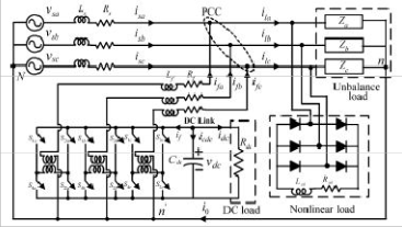
Fig .1. three-phase,four-wire compensated system using the H-bridge
VSI topology-based DSTATCOM.
connected to the PCC through interface inductors. The isolation transformers prevent a short circuit of the dc capacitor for various combinations of the switching states of the VSI. The inductance and resistance of the isolation
transformers are also included in Lf and Rf . The source
voltages are assumed to be balanced and sinusoidal. With
the supply being considered as a stiff source, the feeder
IJSER © 2011 http://www.ijser.org
International Journal of Scientific & Engineering Research Volume 2, Issue 10, Oct-2011 3
ISSN 2229-5518
impedance ( Ls − Rs ) shown in Fig. 1 is negligible and,
hence, it is not accounted in state-space modeling. To track
the desired compensator currents, the VSIs operate under the hysteresis band current control mode due to their simplicity, fast response, and being independent of the load parameters [30]. The DSTATCOM injects currents into the PCC in such a way as to cancel unbalance and harmonics in the load currents. The VSI operation is supported by the dc
storage capacitor Cdc with voltage Vdc across it. The dc bus
voltage has two functions, that is, to support the
compensator operation and to supply dc load. While compensating, the DSTATCOM maintains the balanced
As mentioned before, the source supplies an unbalanced nonlinear ac load directly and a dc load through the dc link of the DSTATCOM, as shown in Fig. 1. Due to transients on the load side, the dc bus voltage is significantly affected. To regulate this dc-link voltage, closed-loop controllers are used. The proportional-
integral-derivative (PID) control provides a generic and
efficient solution to many control problems. The control signal from PID controller to regulate dc link voltage is expressed as
Pdc = Kp (Vdc ref − vdc ) + Ki (Vdc ref − vdc ) dt
![]()
Kd d(Vdc ref − vdc )
sinusoidal source currents with unity power factor and
supplies the dc load through its dc bus.
+ dt
(7)
For the DSTATCOM topology shown in Fig. 1, the
pairs of switches Sla − S2a and S4a − S3a are always ON and
OFF in complimentary mode. The ON and OFF states of
these switches are represented by a binary logic variable Sa
In (7),Kp , Ki , andKd and are proportional, integral,
and derivative gains of the PID controller, respectively. The
proportional term provides overall control action proportional to the error signal. An increase in proportional
controller gain(Kp ) reduces rise time and steady-state error
but increases the overshoot and settling time. An increase
and its complement. Thus, when switches Sla − S2 are ON,
in integral gain K
reduces steadystate error but increases
it implies that switches S4a − S3a are OFF. This is
represented by Sa = 1, S = 0, and vice versa. In a similar
( i )
overshoot and settling time. Increasing derivative gain(Kd )
will lead to improved stability. However, practitioners have
way, Sb , S b , Sc and Sc
and represent gating signals for
often found that the derivative term can behave against
switches Slb − S2b , S4b − S3b , Slc − S2C , S4c − S3c ,respectively.
Using these notations for the system shown in Fig.1 , the
state space equations are written as follows:
x = Ax + Bu (2) Where state vector x and vector u are given by the equations are here
r
x = [ifa ifb ifc vdc ]
anticipatory action in case of transport delay. A cumbersome trial-and-error method to tune its parameters made many practitioners switch off or even exclude the derivative term [31], [32]. Therefore, the description of conventional and the proposed fast-acting dc-link voltage controllers using PI controllers are given in the following
subsections.
(3)
u = [vsa vsb vsc ]r (4)
Where the superscript r stands for the transpose
operator.system matrix(A) and input matrix (B) are given as follows: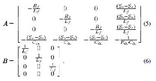
Using the above state-space model, the system state
variables (x) are computed at every instant.
The conventional PI controller used for
maintaining the dc-link voltage is shown in Fig. 2. To maintain the dc-link voltage at the reference value, the dc- link capacitor needs a certain amount of real power, which is proportional to the difference between the actual and reference voltages. The power required by the capacitor can be expressed as follows:
Pdc =
Kp (Vdc ref − vdc ) +
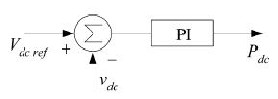
ki ∫(Vdc ref − vdc )dt. (8)
IJSER © 2011 http://www.ijser.org
International Journal of Scientific & Engineering Research Volume 2, Issue 10, Oct-2011 4
ISSN 2229-5518
Fig.2.schematic diagram of the conventional dc-link voltage controller.
controller is the error between the squares of reference and the actual capacitor voltages. This controller is shown in Fig. 3 and the total dc power required by the dc-link
capacitor is computed as follows: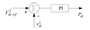
2 − v 2 ) + K
(V2 − v 2 )dt. (11)
Pdc = Kpe (Vdc ref dc
ie dc ref dc
Fig.3. schematic diagram of the fast-acting dc-link voltage controller.
The coefficients Kpe and Kie are the proportional
and integral gains of the proposed energy-based dc-link
voltage controller. As an energy-based controller, it gives fast response compared to the conventional PI controller. Thus, it can be called a fast acting dc-link voltage controller. The ease in the calculation of the proportional and integral gains is an additional advantage. The value of the
proportional controller gain Kpe can be given as
Cdc
Kpe =
2Tc
![]()
(12)
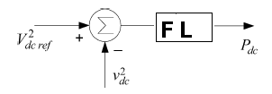
Fig.4. schematic diagram of the fuzzy logic dc-link voltage controller.
The dc-link capacitor has slow dynamics compared to the compensator, since the capacitor voltage is sampled at every zero crossing of phase supply voltage. The sampling can also be performed at a quarter cycle depending upon the symmetry of the dc-link voltage waveform. The drawback of this conventional controller is that its transient response is slow, especially for fast- changing loads. Also, the design of PI controller parameters is quite difficult for a complex system and, hence, these parameters are chosen by trial and error. Moreover, the dynamic response during the transients is totally
dependent on the values of Kp and Ki when Pdc is
For example, if the value of dc-link capacitor is
2200JiF and the capacitor voltage ripple period as 0.01 s,
then is computed as 0.11 by using (12). The selection of
Kie depends upon the tradeoff between the transient
response and overshoot in the compensated source current.
Once this proportional gain is selected, integral gain is
tuned around and chosen to be 0.5. It is found that if Kie is greater than Kpe /2, the response tends to be oscillatory and
if Kie is less than Kpe /2, then response tends to be sluggish.
Hence, Kie is chosen to be Kpe /2.
To overcome the disadvantages of the a forementioned controller, an Fuzzy logic dc-link voltage
controller is proposed. The energy required by the dc-link
comparable to Plavg .
capacitor (Wdcf
)to charge from actual voltage (vdc
) to the
To overcome the disadvantages of the
reference value (Vdc ref f ) can be computed as![]()
Wdcf = 1 Cdc (Vdc ref f − vdc ) (13)
2 2
aforementioned controller, an energy-based dc-link voltage 2
controller is proposed. The energy required by the dc-link
capacitor (Wdc )to charge from actual voltage (vdc ) to the reference value (Vdc ref ) can be computed as
Wdc = 1 Cdc (Vdc ref dc
In general, the dc-link capacitor voltage has ripples
with more than double frequency, that of the supply
frequency. The dc power (Pdc ) required by the dc-link
capacitor is given as![]()
2 − v 2 ) (9)
2
′′ Wdcf 1 2 2
In general, the dc-link capacitor voltage has ripples
with double frequency, that of the supply frequency. The![]()
![]()
Pdc =
Tc =
2Tc
Cdc (Vdc ref f − vdc ) (14)
dc power (P′ ) required by the dc-link capacitor is given as
Where Tc is the ripple period of the dc-link
capacitor voltage. Some control schemes have been
Wdc
2 − v 2 )
reported. However, due to the lack of integral term, there is![]()
′
dc Tc
1
2Tc
Cdc (Vdc ref dc
(10)
Where
Tc is the ripple period of the dc-link
a steady-state error while compensating the combined ac
capacitor voltage. Some control schemes have been reported in [33] and [34]. However, due to the lack of integral term, there is a steady-state error while compensating the combined ac and dc loads. This is eliminated by including an integral term. The input to this
and dc loads. This is eliminated by including an integral
term. The input to this controller is the error between the squares of reference and the actual capacitor voltages. This fuzzy logic controller is shown in Fig. 4 and the total dc power required by the dc-link capacitor is computed as
follows:
IJSER © 2011 http://www.ijser.org
International Journal of Scientific & Engineering Research Volume 2, Issue 10, Oct-2011 5
ISSN 2229-5518
′′ = K
(V2 − v 2 )
Pdc
pe dc ref f
dc
2 − v 2 )dt. (15)
+ Kie (Vdc ref f dc a
The coefficients Kpe and Kie are the proportional
and integral gains of the proposed energy-based dc-link
voltage controller. As an energy-based controller, it gives fast response compared to the conventional PI controller and fast-acting controller. Thus, it can be called a fuzzy logic dc-link voltage controller. The ease in the calculation of the proportional and integral gains is an additional advantage.
The conventional dc-link voltage controller can be designed based on equations given for the fast-acting and fuzzy logic dc-link voltage controller as in (11) and can be
written as
′′ = K (V
+ v )(V
− v )
Pdc
pe dc ref f
dc dc ref f dc
+ Kie (Vdc ref f + vdc )(Vdc ref f
− vdc )dt. (16)
It can also be written as
2 2
′′ = K′ (V
− v )
Where Eer = Vdc ref f − vdc and
Pdc
p dc ref f
dc
+ K′
(Vdc ref f − vdc )dt (17)
![]()
K′
![]()
![]()
K′ (s + i )
Where
K′ = K (V + v ) (18)
′
′′ p
dc
Er =
′
p
s (23)
′
![]()
i
Ki = Kie (Vdc ref f + vdc ) (19)
It is observed from the aforementioned equations
that the gains of proportional and integral controllers vary![]()
Kie
Kpe
Where Er = Vdc ref f − vdc . Since ′ is the same as
p
, the higher gain in the conventional PI controller
with respect to time. However, for small ripples in the dc-
link voltagevdc ≈ Vdc ref , therefore, we can approximate the
above gains to the following:
′
p pe dc ref f
K′ = 2K V . (21)
The relations (17)–(18) give approximate gains for
a conventional PI controller. This is due to the fact that
Vdc ref f + vdc is not really equal to 2Vdc ref f until variation in vdc is small during transients. Hence, the designed
conventional PI controller works only on approximation.
The open-loop gains for the two cases are given by
Kie
renders less stability than that of the proposed energy-
based dc-link controller. For nearly the same performance, the conventional PI controller has gains which are 364 (40/0.11 from Table I) times larger than that of that proposed one. Also, the amplifier units used to realize these gains need more design considerations and are likely to saturate when used with higher gains.
The value of the dc-link capacitor can be selected based on its ability to regulate the voltage under transient
conditions. Let us assume that the compensator in Fig. 1 is
![]()
Pdc
Eer =
![]()
Kpe (s + Kpe )
s (22)
connected to a system with the rating of X kilovolt amperes. The energy of the system is given by X x 1000 J/s.
Let us further assume that the compensator deals with half![]()
System parameters Values
(i.e.,X/2 ) and twice (i.e.,2X ) capacity under the transient conditions for cycles with the system voltage period of T s.
IJSER © 2011 http://www.ijser.org
International Journal of Scientific & Engineering Research Volume 2, Issue 10, Oct-2011 6
ISSN 2229-5518
Then, the change in energy to be dealt with by the dc capacitor is given as
X
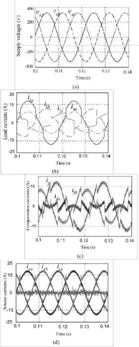
load currents results in neutral current as illustrated in the figure.
The compensator currents and compensated
∆E = 2X −
![]()
nT. (24)
2
source currents are shown in Fig. 4(c) and (d). As seen from
Now this change in energy (21) should be
supported by the energy stored in the dc capacitor. Let us allow the dc capacitor to change its total dc-link voltage
from 1.4Vm to 1.8Vm during the transient conditions where
Vm is the peak value of phase voltage. Hence, we can write
Fig. 4(d), the source currents are balanced sinusoids; however, the switching frequency components are superimposed over the reference currents due to the switching action of the VSI. The currents have a unity
power factor relationship with the voltages in the
C [(1.8V
2 − (1.8V
2
![]()
) ] =
respective phases. The THDs in these currents are 3.6%,![]()
2 dc m m
X
2X − 2 nT (25)
Which implies that![]()
3XnT Cdc =
(1.8Vm )2 − (1.8Vm )2
(26)
3.7%, and 3.9% in phases a, band c respectively. There are
notches in the source currents due to finite bandwidth of
the VSI.
The transient performance of the conventional, fast-acting and fuzzy logic dc-link voltage controllers are
studied by making sudden changes in the ac load supplied
For example, consider a 10-kVA system (i.e., 10
kVA), system peak voltage Vm =325.2 V, n =0.5, and T= 0.02
s. The value of Cdc computed using (23) is 2216 Ji F.
Practically, 2000 JiF is readily available and the same value
has been taken for simulation and experimental studies.
The load compensator with H-bridge VSI topology as shown in Fig. 1 is realized by digital simulation by using MATLAB. The load and the compensator are connected at the PCC. The ac load consists of a three-phase unbalanced load and a three-phase diode bridge rectifier feeding a highly inductive R-L load. A dc load is realized by an
equivalent resistance Rdc as shown in the figure. The dc
load forms 50% of the total power requirement. The system
and compensator parameters are given in Table I.
By monitoring the load currents and PCC voltages, the average load power is computed. At every zero
crossing of phase a voltage, Pdc is generated by using the
dc-link voltage controller. The state-space equations are
solved to compute the actual compensator currents and dc- link voltage. These actual currents are compared with the reference currents given by (1) using hysteresis current control. Based on the comparison, switching signals are generated to compute the actual state variables by solving the state-space model given in (2). The source voltages and load currents are plotted in Fig. 4(a) and (b). The load currents have total harmonic distortions of 8.9%, 14.3%, and
21.5% in phases a, band c, respectively. The unbalance in
by the ac load bus as well as the dc load supplied by the dc link. In the simulation study, the load is halved at the
instant t =0.4 s and brought back to full load at t =0.8 s.
The transient performance is explained in the following
subsections.
The conventional dc-link voltage controller as
given in (8) is used to generate the dc load power Pdc which
is inclusive of losses in the inverter. The transient
performance of the compensator is shown in Fig. 5(a) and (b). The total load, which is a combination of linear unbalanced and nonlinear load (as given in Table I), is
halved at the instant t =0.4 s. Due to a sudden reduction in
the load, the dc-link capacitor absorbs surplus power from
the source. Therefore, there is an increase in dc-link capacitor voltage above the reference value. Based on the values of PI controller gains, the dc-link capacitor voltage controller will be brought back to the reference value after a few cycles.
IJSER © 2011 http://www.ijser.org
International Journal of Scientific & Engineering Research Volume 2, Issue 10, Oct-2011 7
ISSN 2229-5518
link voltage controller are not properly chosen, the dc-link voltage would have undesirable overshoot and considerably large settling time. Consequently, the performance of the load connected to the dc link also gets affected due to the above factors. It can be observed from Fig. 5(a) and (b) that the conventional dc-link voltage controller takes about a ten cycle period to reach the reference voltage during load transient. This is indicated by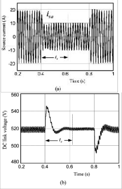
time duration ts in these figures.
Fig. 5.Transient response of the conventional controller. (a) Compensated source current in phase a. (b) DC-link voltage.
Fig. 4. (a) Supply voltages. (b) Load currents. (c) Compensator currents. (d) Compensated source currents.
Similarly, when the load is switched back to the
full load at instant t =0.8 s, the dc capacitor supplies power
to the load momentarily and, hence, the dc-link voltage
falls below the reference value. Due to the PI controller action, the capacitor voltage will gradually build up and reach its reference value. If gains of the conventional dc-
The dc load power Pdc is computed by using the
fast-acting dc-link voltage controller as given in (11).
Transients in the load are considered the same as in the above simulation study. Fig. 6(a) and (b) illustrates the
phase a source current and dc-link capacitor voltage during
the load transients.
At the instant t = 0.4 s, the capacitor voltage
increases due to the sudden removal of the load. The fast-
acting dc-link voltage controller takes action at the instant
t =0.44 s. This is because the controller output is updated at every half cycle. It computes the dc load power Pdc needed
to bring the capacitor voltage to the reference value in a
half cycle. Therefore, the dc-link voltage reaches its
reference voltage at the instant t =0.42 s. When the dc-link voltage is more than the reference value, Pdc is less.
Therefore, the source currents are less in magnitude.
IJSER © 2011 http://www.ijser.org
International Journal of Scientific & Engineering Research Volume 2, Issue 10, Oct-2011 8
ISSN 2229-5518
At the instant t = 0.8 s, the dc-link voltage falls
below the reference voltage due to a sudden increase in
load. As explained earlier, the fast-acting controller brings
the dc-link voltage to its reference value at t =0.84 s with
every half cycle. It computes the dc load power P′′ needed
to bring the capacitor voltage to the reference value in a
half cycle. Therefore, the dc-link voltage reaches its
reference voltage at the instant t =0.415 s. When the dc-link
′′
almost the same rise in voltage as that of the conventional
dc-link voltage controller. A close observation of the figure
voltage is more than the reference value, Pdc
Therefore, the source currents are less in magnitude.
is less.
would reveal that the fast-acting dc-link voltage controller can regulate the capacitor voltage within a half cycle period
which is indicated by ts . Owing to its good transient
performance, it is preferred over the conventional dc-link
voltage controller.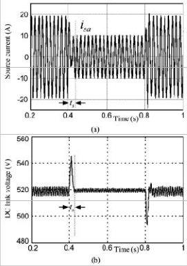
Fig. 6. Transient response of the fast-acting controller. (a) Compensated source current in phase a. (b) DC-link voltage.
The dc load power P′′ is computed by using the
fuzzy logic dc-link voltage controller as given in (11).
Transients in the load are considered the same as in the above simulation study. Fig. 7(a) and (b) illustrates the
phase a source current and dc-link capacitor voltage during
the load transients.
At the instant t = 0.4 s, the capacitor voltage
increases due to the sudden removal of the load. The fuzzy
logic dc-link voltage controller takes action at the instant
t =0.41 s. This is because the controller output is updated at
At the instant t = 0.8 s, the dc-link voltage falls
below the reference voltage due to a sudden increase in
load. As explained earlier, the fast-acting controller brings
the dc-link voltage to its reference value at t =0.81 s with
almost the same rise in voltage as that of the conventional
dc-link voltage controller. A close observation of the figure would reveal that the fuzzy logic dc-link voltage controller can regulate the capacitor voltage within a half cycle period
which is indicated by ts . Owing to its good transient
performance, it is preferred over the conventional and fast-
acting dc-link voltage controller.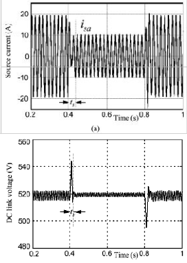
(b)
Fig. 7. Transient response of the fuzzy logic controller. (a) Compensated source current in phase a. (b) DC-link voltage.
To verify the effectiveness of the proposed energy based dc link voltage controller for the DSTATCOM, a three-phase prototype model has been developed in the laboratory. The overall block diagram of the hardware set- up is shown in Fig. 8(a), the control hardware setup is shown in Fig. 8(b) and the power circuit of the DSTATCOM
IJSER © 2011 http://www.ijser.org
International Journal of Scientific & Engineering Research Volume 2, Issue 10, Oct-2011 9
ISSN 2229-5518
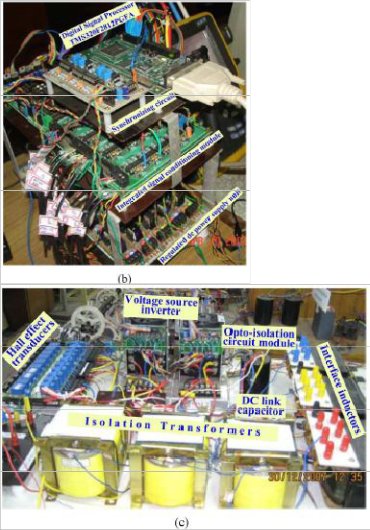
is shown in Fig. 8(c). The three phase power quantities
(voltages and currents) are converted to
low-level voltage signals using the Hall effect voltage and current transducers. These signals are further conditioned by using signal conditioning circuits and are given to the analog-to-digital converter (ADC) channels of the digital signal processor (DSP) TMS320F2812PGFA. The DSP also receives a signal from the synchronizing circuit to realize reference quantities in time domain. The DSP is connected to the host computer
through a parallel port. The control algorithm in the DSP
generates switching pulses to the VSI. These pulses are then passed through the blanking circuit to include dead time in order to prevent the short circuit of the capacitor through switches in the same VSI leg. The blanking circuit also receives STOP signals from the protection circuit to ensure safe operation of the DSTATCOM in case of any abnormality in the system. The
blanking circuit output pulses are given to the VSI through
the opto isolator circuit to isolate the high-power network and the signal-level circuits.
The ac load consists of a three-phase unbalanced load and a three-phase diode bridge rectifier feeding a highly inductive R-L load. A resistance connected in the dc link is considered as dc load. The compensator consists of
12 IGBT switches each with anti parallel diodes in two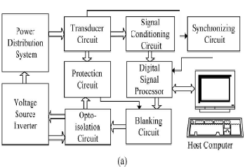
intelligent power modules (PM50RVA120), three isolation transformers, and three external interface inductors. The system parameters for the experimental setup are given in Table II.
Fig. 8.Experimental setup. (a) Block diagram of the hardware setup. (b) Control hardware setup. (c) Power circuit of the H-bridge VSI-based DSTATCOM.
The average load power is computed by taking the samples of the load currents and PCC voltages. The dc load
power (P′′ ) is generated by using the conventional dc-link
voltage controller and fast-acting dc-link voltage
controllers. Based on these values, reference compensator currents are obtained by using (1).
The VSI is then operated in the hysteresis band current control mode to synthesize the actual compensator currents. Accordingly, the switching commands are issued to control IGBT switches through proper interfacing
circuits.
IJSER © 2011 http://www.ijser.org
International Journal of Scientific & Engineering Research Volume 2, Issue 10, Oct-2011 10
ISSN 2229-5518
System parameters | Values |
Supply voltage | 76 v(L-L),50Hz |
Unbalanced load | Za = 11 + ]12.5Ω Zb =12+j12.5Ω Zb = 14.5 + j18.8Ω |
Nonlinear load | Three-phase full wave rectifier feeding an R-L load of 82.512, 60 mH. |
DC load | Rdc = 10012 |
DC capacitor | Cdc = 2000JiF |
Interface inductor | Lf = 20mA, Rf = 1.012 |
Reference dc link voltage | Vdc ref = 100V |
Hysteresis band | ±ℎ = 0.16A |
Gains of conventional dc link Voltage controller | Kp = 10, Ki = 1.0 |
Gains of fast acting dc link Voltage controller | Kp = 0.11, Ki = 0.055 |
Gains of fuzzy logic dc link voltage controller | Kp = 0.015 , Ki = 0.0052 |
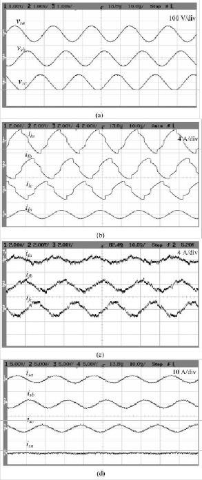
The source voltages and load currents are shown in Fig.9(a) and (b), respectively. The source voltages are balanced and sinusoidal but the load currents have both unbalance and distortions. The unbalance in load currents results in neutral current. The THDs of the load currents are
11.6%, 16.7%, and 24.2% in phases a, b andc, respectively.
Compensator and compensated source currents are shown
in Fig. 9(c) and (d) respectively. The source currents are balanced sinusoids with the THDs of 5.2%, 4.8%, and 4.7%
in phases a, b andc, respectively. Fig.9. (a) Supply voltages. (b) Load currents. (c) Compensator currents.
(d) Source currents after compensation.
The transient performance with the conventional dc-link voltage controller is shown in Fig. 10. At an
instantt = tl , the unbalanced linear R-L load and a half dc load are removed. At t = tl , the load is brought to its original value. The power(Pdc ) required by the dc link is
computed by using (8). Fig. 10 illustrates the compensated
IJSER © 2011 http://www.ijser.org
International Journal of Scientific & Engineering Research Volume 2, Issue 10, Oct-2011 11
ISSN 2229-5518
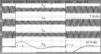
source currents and dc-link voltage. From this figure, it can be understood that the use of the conventional controller with an improper value of controller gains cannot bring the actual dc-link voltage to its reference value quickly. It takes around 40 cycles to regulate the dc-link voltage to its reference voltage.
Fig. 10. Source currents and dc-link voltage with a conventional dc-link voltage controller.
The performance of the fast-acting dc-link voltage controller is tested by using the transient load used in the previous section. Fig. 10 shows the source currents during the transients in load by using this fast-acting dc-link voltage controller as given in (11). From the close observation of the figure, it is found that the response time is very less compared to that of the conventional dc-link voltage controller. Though, in simulation studies, the fast- acting voltage controller corrects the actual dc-link voltage in a half cycle, the experimental results do not fully validate the same. This is due to the use of the mechanical switch for the change of load, which cannot connect/disconnect the
load in all three phases simultaneously at the instants tl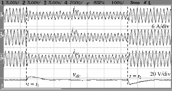
andt2, and due to other non idealities in the system.
Fig. 11. Source currents and dc-link voltage with a fast-acting dc-link voltage controller.
The transient performance of the fuzzy logic dc- link voltage controller is tested by using the transient load used in the previous section. Fig. 11 shows the source currents during the transients in load by using this fuaay logic dc-link voltage controller as given in (12). From the close observation of the figure, it is found that the response time is very less compared to that of the conventional and fast-acting dc-link voltage controller. Though, in simulation studies, the fuzzy logic voltage controller corrects the actual dc-link voltage in a half cycle, the experimental results do not fully validate the same. This is due to the use of the mechanical switch for the change of load, which cannot connect/disconnect the load in all three phases
simultaneously at the instants tl andt2 , and due to other
non idealities in the system.
There is slight change in the fuzzy logic dc-link voltage control as compared to the fast-acting dc-link voltage control. but, more change will be seen when compared to the conventional dc-link voltage control.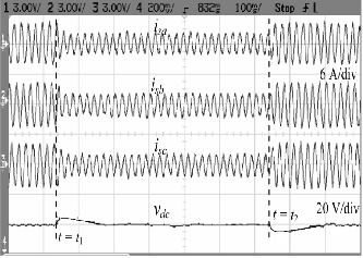
Fig. 12. Source currents and dc-link voltage with a fast-acting dc-link voltage controller.
A VSI topology for DSTATCOM compensating ac unbalanced and nonlinear loads and a dc load supplied by the dc link of the compensator is presented. The state-space modeling of the DSTATCOM is discussed for carrying out the simulation studies. An energy-based fuzzy logic dc-link voltage controller is suggested to ensure the fast transient response of the compensator. Mathematical equations are developed to compute the gains of this controller. The
efficacy of the proposed controller over the conventional
IJSER © 2011 http://www.ijser.org
International Journal of Scientific & Engineering Research Volume 2, Issue 10, Oct-2011 12
ISSN 2229-5518
and fast-acting dc-link voltage controller is established through the digital simulation and experimental studies. It is observed from these studies that the proposed dc-link voltage controller gives fast transient response under load transients by using the fuzzy logic controller.
REFERENCES
[1] M. H. J. Bollen, Understanding Power Quality Problems: Voltage Sags and Interruptions. New York: IEEE Press, 1999.
[2] W. M. Grady and S. Santoso, Proc. IEEE Power Eng. Rev.
Understanding Power System Harmonics, vol. 21, no. 11, pp. 8–11,
2001
[3] N. Hingorani, “Introducing custom power,” IEEE Spectr., vol. 32, no. 6, pp. 41–48, Jun. 1995.
[4] A. Ghosh and G. Ledwich, Power Quality Enhancement Using
Custom Power Devices. Norwell, MA: Kluwer, 2002.
[5] V. Dinavahi, R. Iravani, and R. Bonert, “Design of a real-time digital simulator for a D-STATCOM system,” IEEE Trans. Ind. Electron., vol. 51, no. 5, pp. 1001–1008, Oct. 2004.
[6] D. Vilathgamuwa, H. M.Wijekoon, and S. S. Choi, “A novel technique to compensate voltage sags in multiline distribution system and the interline dynamic voltage restorer,” IEEE Trans. Ind.Electron., vol. 55, no. 5, pp. 1603–1611, Oct. 2006.
[7] H. Akagi, Y. Kanazawa, and A. Nabae, “Instantaneous reactive power compensators comprising switching devices without
energy storage components,” IEEE Trans. Ind. Appl., vol. IA-20, no.
3, pp. 625–630, May 1984.
[8] H. Kim, F. Blaabjerg, B. B. Jensen, and J. Choi, “Instantaneous Power compensation in three-phase systems by using p-q-r theory,” IEEE Trans. Power Electron., vol. 17, no. 5, pp. 701–709, Sep. 2002.
[9] F. Z. Peng and J. S. Lai, “Generalized instantaneous reactive power Theory for three-phase power systems,” IEEE Trans. Instrum. ., vol. 45, no. 1, pp. 293–297, Feb. 1996.
[10] T. Furuhashi, S. Okuma, and Y. Uchikawa, “A study on the theory of in stantaneous reactive power,” IEEE Trans. Ind. Electron., vol.
. 37, no 1, pp. 86–90, Feb. 1990.
[11] A. Ghosh and A. Joshi, “A new approach to load balancing and power factor correction in power distribution system,” IEEE Trans. Power Del., vol. 15, no. 1, pp. 417–422, Jan. 2000.
[12] S. Kim, M. H. Todorovic, and P. N. Enjeti, “Three-phase active harmonic rectifier (AHR) to improve utility input current THD telecommunication power distribution system,” IEEE Trans. Ind. Appl., vol. 39,no. 5, pp. 1414–1421, Sep./Oct. 2003.
[13] R. Redl and A. S. Kislovski, “Telecom power supplies and power quality,” in Proc. 17th Int. Telecommunications Energy Conf., Denmark,Oct. 29–Nov. 1 1995, pp. 13–21.
[14] M. M. Jovanovic and Y. Jang, “State-of-the-art, single-phase active power-factor-correction techniques for high-power applications—An overview,” IEEE Trans. Ind. Electron., vol. 52, no. 3, pp. 701–708, Jun.2005.
[15] A. S. Kislovski, “Telecom power-supply plants using three-phase rectifiers and active filters,” in Proc. 2nd Int. Telecommunications
Energy Special Conf., Budapest, Hungary, Apr. 22–24, 1997, pp.
[16] P. Verdelho and G. D. Marques, “DC voltage control and stability analysis of PWM-voltage-type reversible rectifiers,” IEEE Trans. Ind. Electron.,vol. 45, no. 2, pp. 263–273, Apr. 1998.
[17] A. Prodic´ and G. D. Marques, “Compensator design and stability Assessment for fast voltage loops of power factor correction rectifiers,” IEEE Trans. Power Electron., vol. 22, no. 5, pp. 1719–
1730, Sep. 2007.
[18] D. Zhao and R. Ayyanar, “Space vector PWM with DC link voltage control and using sequences with active state division,” in Proc., IEEE Int. Symp. Industrial Electronics, Montreal, QC, Canada, Jul. 9–12, 2006, vol. 2, pp. 1223–1228.
[19] K. Mahabir, G. Verghese, J. Thottuvelil, and A. Heyman, “Linear averaged and sampled data models for large signal control of high power factor AC-DC converters,” in Proc. 21st IEEE Power Electronics Specialists Conf., Jun. 1990, pp. 372–381.
[20] M. O. Eissa, S. B. Leeb, G. C. Verghese, and A. M. Stankovic´,
“Fast controller for a unity power factor rectifier,” IEEE Trans. Power Electron.,vol. 11, no. 1, pp. 1–6, Jan. 1996.
[21] M. K. Mishra, A. Ghosh, and A. Joshi, “A new STATCOM topology to compensate loads containing ac and dc components,” in Proc. IEEE Power Eng. Soc. Winter Meeting, Singapore, Jan. 23–
27, 2000, vol. 4, pp. 2636–2641.
[22] A. Nabae, I. Takahashi, and H. Akagi, “A new neutral-point- clamped PWM inverter,” IEEE Trans. Ind. Appl., vol. IA-17, no. 5, pp. 518–523,Sep. 1981.
[23] M. Aredes, J. Häfner, and K. Heumann, “Three-phase four-wire shunt active filter control strategies,” IEEE Trans. Power Electron., vol. 12,no. 2, pp. 311–318, Mar. 1997.
[24] C. A. Quinn, N. Mohan, and H. Mehta, “Active filtering of harmonic currents in three-phase, four-wire systems with three- phase and sing phase non-linear loads,” in Proc. Applied Power x phase and sing pp. 829–836.
[25] B. Singh, K. Al-Hadded, and A. Chandra, “A review of active filters for power quality improvements,” IEEE Trans. Ind. Electron., vol. 46, no. 5, pp. 960–971, Oct. 1999.
[26] M. El-Habrouk, M. K. Darwish, and P. Mehta, “Active power filters: A review,” Proc. Inst. Elect. Eng., Electr. Power Appl., vol.
147, no. 5, pp. 403–413, Sep. 2000.
[27] A. Dell’Aquila, M. Liserre, V. G. Monopoli, and P. Rotondo, “An energy-based control for an n-H-bridges multilevel active rectifier,” IEEE Trans. Ind. Electron., vol. 52, no. 3, pp. 670–678, Jun. 2005.
[28] S. Iyer, A. Ghosh, and A. Joshi, “Inverter topologies for DSTATCOM applications—A simulation study,” Elect. Power p. Syst. Res., vol. 75, p161–170, Aug. 2005.
[29] B.-R. Lin and C.-H. Huang, “Implementation of a three-phase capacitor-clamped active power filter under unbalanced condition,” IEEE Trans. Ind. Electron., vol. 53, no. 5, pp. 1621–1630, Oct. 2006.
[30] M. P. Kazmierkowski and L. Malesani, “Current control techniques for three-phase voltage-source PWM converters: a. survey,” IEEE Trans Ind. Electron., vol. 45, no. 5, pp. 691–703, Oct.
1998.
[31] K. H. Ang, G. Chong, and Y. Li, “PID control system analysis, design, and technology,” IEEE Trans. Control Syst. Technol., vol..
13, no. 4, pp 559–576, Jul. 2005.
[32] R. Ortega and R. Kelly, “PID self-tuners: Some theoretical and practical aspects,” IEEE Trans. Ind. Electron., vol. IE-31, no. 4, pp.
332–338, Nov. 1984.
[33] B. N. Singh, P. Rastgoufard, B. Singh, A. Chandra, and K. Al-
IJSER © 2011 http://www.ijser.org
International Journal of Scientific & Engineering Research Volume 2, Issue 10, Oct 2011 13
ISSN 2229 5518
Haddad, "Design, simulation and implementation of three pole/four pole topologies for active filters," Proc. Inst. Elect. Eng., Electr. Power Appl., voL 151, no. 4, pp. 467--476, Jul. 2004.
[34] Y. Ye, M. Kazerani, and V. Quintana, "Modeling, control and
implementation of threephase PVVM converters," IEEE Trans. Power Electron.,voL 18, no. 3, pp. 857-864, May 2003.
IJSER ©2011
http://www.ijserora