International Journal of Scientific & Engineering Research, Volume 3, Issue 2, February-2012 1
ISSN 2229-5518
A Detailed Computer Analysis of SiC And GaN Based IMPATT Diodes Operating at Ka, V And W
Band
D. Ghosh, B. Chakrabarti, M. Mitra
Abstract:- From 1965 onwards lot of developments and simulation works have been done in the field of IMPATT diode to improve its power output, efficiency and frequency range of operation using low band gap material like Si, GaAs, InP etc. In this paper a comprehensive study has been made on IMPATT diodes based on high band gap materials, GaN (Wz) and SiC (4H) operating at Ka, V and W-band respectively relative to fabrication and it has been found that SiC based IMPATT gives improved performance at low frequency bands whereas GaN based IMPATT’s show better response at higher frequency bands. Efficiency around 23% is obtained from SiC IMPATT and about 17% for GaN IMPATT diode. In general the power frequency relation for any device is inverse, but power decreases at a faster rate in case of SiC IMPATT than a GaN IMPATT with the increase of frequency.
Index Terms: SiC IMPATT, GaN IMPATT, RF power, Negative conductance, Ka band IMPATT diode, V band IMPATT diode and W band IMPATT
diode
1 INTRODUCTION
IMPACT avalanche transit time (IMPATT) diode are considered to be one of the most powerful solid state sources operating in the mm-wave and sub-mm wave frequencies. Among all solid state devices IMPATT diodes are the most efficient RF power generators. These two terminal active devices have the capability to deliver high RF power even at THz frequency range [1, 2].
Extensive analysis has already being done on low band gap
materials such as Si (IVth group element), GaAs (III-Vth) compound semiconductors and its compound alloy heterostructure materials. In recent years, wide band gap semiconductors specially GaN and SiC have emerged as promising materials for the development of high power (watt level) IMPATT devices due to their unique physical and electronic properties such as direct band gap structure, high electric breakdown field and high thermal conductivity. High breakdown voltage and high thermal conductivity are the essential requirements for high power operation and

D. Ghosh is currently working as asst. prof. in the Dept. of Electronics & Communication Engineering, Swami Vivekananda Institute of Science and Technology, Kolkata-145, India. E-mail: dg1036@yahoo.com
B.Chakrabarti is currently working as asst. prof. in the Dept. of Electronics & Communication Engineering, Bengal Institute of Technology, Kolkata150, India. E-mail: chakrabortybibek@yahoo.co.in
M. Mitra is currently working as associate prof. in the Dept. of
Electronics & telecommunication, BESU, Shibpur, Howrah
711103,W.B., India. E.mail:- monojit_m1@yahoo.co.in
good thermal stability. Moreover from the fabrication point of view high quality GaN film can be grown on SiC substrate by metal organic chemical vapor deposition (MOCVD) [3]. In addition to this, significant development has also been achieved recently in 4H-SiC growth, processing and characterization. The feasibility of designing IMPATT devices with wide band gap materials such as SiC, GaN and compounds based on it has been established. Some theoretical as well as experimental results on SiC-based IMPATTs are also reported in recent literature [2].
The two common types of GaN are, Wurtzite and Zinc-blend
.Wurtzite phase GaN (Wz) based IMPATTs have found to perform better than Zinc-blend (ZnB) GaN, in terms of breakdown voltage, efficiency and power output at around
140 GHz [4].Among all the polytypes of SiC the availability
of good quality single crystal wafers of α (4H and 6H) SiC makes these polytypes the important materials for electronic devices. It has been found that 4H-SiC has substantially higher carrier mobility compared to 6H-SiC.Further the anisotropy of carrier mobility degrades the performance of
6H-SiC.Moreover it is already reported that the high frequency performance of 4H-SiC IMPATT is far better than its 6H-SiC counterpart in terms of breakdown voltage (VB) as well as PRF [5].The detail analysis on the dc and small signal properties of GaN (Wz) and SiC (4H) IMPATT diodes and their comparative studies have not been reported so far in recent literatures. Separate studies on the various mm-wave frequency bands of the devices are therefore necessary to
IJSER © 2012 http://www.ijser.org
International Journal of Scientific & Engineering Research, Volume 3, Issue 2, February-2012 2
ISSN 2229-5518
evaluate the device performances and suitability of the type of materials in any specified band.
In this paper the authors have studied the performances of GaN-based IMPATT diodes and compare the results with SiC based IMPATT diodes operating under similar conditions at different mm-wave frequency bands (ka-band, v-band and w-band) and stabilized the potentiality of GaN- based devices for high frequency operation.
Table 1
Material parameters of GaN and SiC polytypes (at
300K).
were designed following an IMPATT/MITATT mode dc simulation scheme [6] that determines dc properties of the diodes. The high frequency properties of the diodes were then computed following MITTAT mode small signal simulation scheme. The final solutions of dc simulation were used to determine the microwave characteristics. In this paper the small signal characteristics includes susceptance, negative conductance and also negative resistance of the device. Then for a known area of the diode and negative conductance, using the procedure described in literature [6], the RF power generated from the device was computed. For the present analysis experimental values of carrier ionization rates , temperature dependent (300k<T<600k) values of drift velocities and mobilities of charge carriers in GaN (Wz) and SiC (4H) are considered for the simulation work [8,9,10]. All the material parameters values which have been considered for simulation are summarized in table1.
Table 2
Design parameters
2 MATERIAL PARAMETERS & SIMULATION METHOD
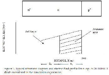
For analysis purpose a flat profile SDR (n+ n p+) structures is considered as shown in figure 1. The device dimensions, doping level and current densities for both types of diodes (Wz-GaN and 4H-SiC) are optimized at Ka, V and W
frequency bands after several computer runs. The devices
IJSER © 2012 http://www.ijser.org
International Journal of Scientific & Engineering Research, Volume 3, Issue 2, February-2012 3
ISSN 2229-5518
2.1 DC Analysis
The dc method has already been described in details elsewhere [7] considered a generalized n++ n p p++ structure. The author has followed the same method with the exception of n+ n p+ SDR structure instead of a DDR one. Here n+ and p+ are highly doped substrate and n is an epilayer. In the dc method, the numerical computation starts from the field maximum near the metallurgical junction. The distribution of dc electric field and carrier currents in the depletion layer are obtained by a double iterative simulation method, which involves iteration over the magnitude of field maximum (Em) and its location in the depletion layer. At each point in the depletion layer simultaneous solutions of Poisson and carrier continuity equations are used in this method. The field boundary conditions are given by,
E(-x1)=0 and E(+x2)=0 (1)
Here –x1 and x2 represent the edges of the depletion layer in n and p regions, respectively.
The boundary conditions for normalized current density
P(x), are given by,
P(-x1)=(2/Mp - 1) and P(x2)=(1 – 2/Mn) (2)
Where Mn = J/Jns, Mp = J/Jps ;Jns and Jps are electron and hole leakage current densities, respectively.
satisfied. The realistic field dependence of electron and hole ionization rates, carrier mobility and the saturated drift velocities of electron and hole are used in the computation for the profile of electric field and carrier currents.
The dc to mm-wave conversion efficiency is calculated from the approximate formula,
η (%) = (VD x 100)/(π x VB) (3)
Where, VD=voltage drop across the drift region. Also VD= VB
– VA, where VA = voltage drop across the avalanche region, and VB = breakdown voltage.
VB =  (4) Where –x1 = n-side depletion layer width
And +x2 = p-side depletion layer width
The results of the dc analysis are then used in the small signal analysis, described briefly in the next sub-section.
2.2 Small signal analysis
The Gummel-Blue method [11] has been followed to compute the negative conductance of the diode at different frequency bands. The dc electric field and current profiles, which are obtained from the D.C analysis, are fed as input data for the small signal analysis. The real part R(x, ω) and imaginary part X(x, ω) are obtained by splitting the diode impedance Z(x, ω) using Gummel-Blue method and thus two different equations are framed [6]. Then, by using modified Runga-Kutta method the solutions of these two equations are found following a double iterative simulation scheme. The small signal parameters like negative conductance(-G), susceptance (B), impedance (Z) of the diode and the range of frequencies over which the diode exhibits negative conductance are found after satisfying the boundary conditions derived elsewhere [12,13].
The diode negative resistance (-ZR) and reactance (-Zx) are computed through numerical integration of the –R(x) and
–X(x) profiles over the active space charge layer. Thus
Mn and Mp are hole and electron current multiplication factors, respectively.
-ZR


= and -Zx =
P=(Jp-Jn)/J, where Jp = hole current density , Jn = electron current density and J total current density.
Thus the dc field and carrier current profiles are obtained by simultaneously solving Poisson and carrier continuity
equations, when boundary conditions (1) and (2) are
The diode impedance Z is given by,
Z(ω) =  = -ZR +jZx (5) The diode admittance is expressed as
IJSER © 2012 http://www.ijser.org
International Journal of Scientific & Engineering Research, Volume 3, Issue 2, February-2012 4
ISSN 2229-5518
Y = 1/Z = -G + jB = 1/(-ZR + jZx)
where, -G = -ZR/((ZR)2 + (Zx)2 ) and
B=Zx/((ZR)2 + (Zx)2) (6)
-G and B are both normalized to the area of the diode.
The Avalanche (resonance) frequency (fa) is a frequency at which the imaginary part, susceptance (B) of the admittance changes its nature from inductive to capacitive. The small signal quality factor (Qp) is defined as the ratio of the imaginary part of the admittance (at the peak frequency), i.e.
-Qp= (Bp/-Gp) (7)
At a given bias current density, the peak frequency (fp) is the frequency at which the magnitude of the negative conductance of the diode is maximum, and the quality factor is minimum. At fp, the maximum RF power (PRF) from the device is obtained from the expression [13].The area of the diode is considered to be 5x10-11 m2. Under small signal condition VRF (the amplitude of the RF swing) is taken as VB/5[14,15].
3 RESULT & DISCUSSIONS
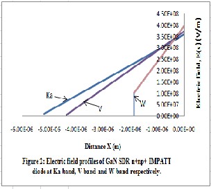
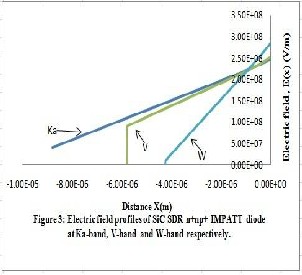
The optimized design parameters of both GaN (Wz) and SiC (4H) SDR IMPATT diodes at different mm-wave frequency bands are summarized in table2. The DC properties of GaN (Wz) and SiC (4H) are presented in the table 3 and the results of GaN (Wz) show a close resembles with the already published work [16,17]. It is observed that the value of peak electric field (Em) at the junction is more for GaN (Wz) diodes than SiC (4H) diodes at all the operating frequency bands of consideration. It is interesting to observe that the Avalanche zone is much more localized for low frequency operation of the diodes which actually contribute to the higher value of efficiency of the diode .The efficiency of SiC diodes are computed as 23.28% (Ka band) , 21.34%( V band) and 20.55% (W band) respectively. Comparing the breakdown voltage it has been observed that GaN IMPATT diodes operate at lesser value of voltages in comparison of their SiC counterpart at all the frequency bands.
.
Table 3
IJSER © 2012 http://www.ijser.org
International Journal of Scientific & Engineering Research, Volume 3, Issue 2, February-2012 5
ISSN 2229-5518
DC and small signal analysis results
Material | Design band | Em (108 Vm-1) | VD (V) | VB (V) | η (%) | -GP (106 Sm-2) | BP (106 S- 2) | Pout (w) | -QP |
4H-SiC | Ka | 2.47 | 914 | 1250 | 23.28 | 2.29 | 2.96 | 3.57 | 1.29 |
4H-SiC | V | 2.52 | 654 | 975 | 21.36 | 3.01 | 5.5 | 2.86 | 1.82 |
4H-SiC | W | 2.86 | 320 | 496 | 20.55 | 3.52 | 14.1 | 0.86 | 4.00 |
Wz- GaN | Ka | 3.59 | 532 | 945 | 17.93 | 1.60 | 2.78 | 1.42 | 1.73 |
Wz- GaN | V | 3.75 | 370 | 650 | 17.79 | 3.44 | 5.76 | 1.45 | 1.67 |
Wz- GaN | W | 3.95 | 188 | 367 | 16.31 | 6.44 | 22.8 | 0.867 | 3.54 |
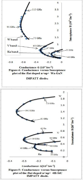
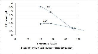
Considering the d.c performances in term of breakdown voltage, efficiency ect. it may be observed that SiC based IMPATTs perform better than GaN based IMPATTs. High frequency analysis was carried out of the devices under same design and operating conditions and the corresponding results are shown in table3.The admittance characteristics of both types of diodes at different mm-wave frequency bands are shown in figure 4 and 5 respectively. The peak operating frequencies (fp) are found to be almost same at Ka-band and V-band for both SiC and GaN diodes. It is also observed that in W-band fp is 91 GHz for GaN and
94.5 GHz for SiC diode which shows an upward shift of 4.5
GHz. Considering the RF power, PRF value is much higher for 4H-SiC SDR diode, at Ka-band and V band respectively than GaN counterpart. The present study also reveals that the RF power contributed by 4H-SiC SDR decreases significantly with the increase in frequency of operation. The same decreasing nature of the PRF in case of Wz-GaN SDR diode is also observed (figure 6). In the case of Wz-GaN SDR diode, the decreasing rate is very slower than that in SiC diodes. It is interesting to see that at W-band GaN based diode perform better than SiC based diode in term of RF power generation. Considering the quality factors (Qp) it has been seen (Table3) that Ka band diodes give better response than other two bands that is V-band and W-band for both types of diodes materials. In addition to this it is also observed that GaN based diode performs superior than their SiC counterpart at W- band in terms of Quality factor.
IJSER © 2012 http://www.ijser.org
International Journal of Scientific & Engineering Research, Volume 3, Issue 2, February-2012 6
ISSN 2229-5518
Therefore taking into account the RF power and quality factor, GaN based SDR IMPATT‟s shows better performance at high operating frequency bands at a particular current density .
4 CONCLUSION
The simulation experiment demonstrates the suitability of using SiC (4H) and GaN (Wz) for fabrication of high frequency electronic devices. The investigation revealed that SiC(4H) IMPATT diodes give superior performance in terms of d.c and small signal properties at Ka-band and V- band respectively compared to IMPATT diodes fabricated from GaN (Wz). As the frequency of operation increases that is at W-band GaN (Wz) IMPATT diode provides improved performance as compared to SiC (4H) IMPATT diode. The present analysis may be found to be extremely helpful for the selection of high band gap material to fabricate IMPATT diode at different mm-wave frequency bands of operation.
REFERENCES
[1] Mukherjee M, Roy S K „‟wide band gap III-V transit time diode in terahertz regime: studies on the effects of punch through on high frequency characteristics and series resistance of the device‟ Current Applied Physics 10(2010) 646-651.
[2] Mukherjee M, Majumder N „‟Effects of charge bump on high frequency characteristics of α-SiC based double drift ATT diodes at millimeter wave window frequencies‟‟IETE journal of research,vol-
55,issue 3,118-126
[3] Inoki CK, Kaun TS, LEE CD, Sagar A, Feenstra RM, Koleske DD, Dfaz DZ, Bohn W and Adesida I , Growth of GaN on porous SiC and GaN substrates Journal for Electron Material, vol. 32, pp 855, 2003.
[4] Panda A K, Pavlidis D and Alekseev E „‟DC and High-frequency Characteristics of GaN based IMPATT ‟‟ 2001 IEEE Trans.Eletron Devices 48 820
[5] Mukherjee M , „‟Effects of optical illumination on 4H-SiC DDR IMPATT diodes at 140 GHz‟‟. CODEC 06, pp.298-301, Kolkata, India, December 2006.
[6] S.M.Sze, Physics of Semiconductor Devices, second ed., Wiley
Eastern Limited, 1991
[7] Mukherjee M, Majumder N, Roy S K and Goswami K “GaN IMPATT Diode: a photo sensitive high power terahertz source” Semicond. Sci.Technol. 22(2007) 1258-1267
[8] Electronic Archive. New Semiconductor Materials. Characteristics and properties http://www.ioffe.ru/SVA/NSM/Semicond/GaN
[9] W.S.Loh,B.K.Ng,J.S.Ng,‟‟Impact Ionisation Coefficients in 4H-SiC‟‟
IEEE Electron Devices,vol.55,No.8,August 2008.
[10] Kunihiro K,Kasahara K, Takahashi Y and Ohno Y “Experimental evaluation of impact ionization coefficients in GaN”,1999 IEEE Electron Device Lett. 20 608
[11] Gummel H K and Blue J L “Small Signal Theory of Avalanche
Noise in IMPATT diodes”,1967 IEEE Trans.Eletron Devices 14 569
[12] Mukherjee M, Roy S K “Wide band gap III-IV nitride based avalanche transit time diode in terahertz regime: studies on the effects on punch through on high frequency characteristics and series resistance of the device”Current Applied Physics 10(2010) 646-651
[13] Eisele H and Haddad G I 1997 Active microwave Devices
Microwave Semiconductor Device Physics ed S M Sze (New York) p 343
[14] Mazumder N and Roy S K “Studies on pulsed mm-wave low- high-low Si IMPATT diodes at high current density and dependence on structural parameters”997 Semicond. Sci.Technol. 12 623
[15] Mazumder N, Banerjee J P and Roy S K “Variation of high frequency negative resistance of silicon n+pp+ and GaAs p+nn+ IMPATT diodes with enhancement of reverse saturation current ”,1989
Phys. Status Solidi A 116 415
[16] Chakrabarti B, Ghosh D, Mitra M „‟High frequency performance Of
GaN based IMPATT Diodes‟‟IJEST, vol.3, No.8, august.2011, 6153-6159
[17] Mukherjee M, Mazumder N and Roy S K “Photo-sensitivity analysis of GaN and SiC terahertz IMPATT oscillator : comparison on theoretical reliability and study on experimental feasibility” IEEE Trans. Device Mater Reliab. 8 (2008) 608- 620
IJSER © 2012 http://www.ijser.org