International Journal of Scientific & Engineering Research, Volume 5, Issue 7, July-2014 1061
ISSN 2229-5518
A Comparative Analysis of conventional inverter with multilevel inverter - a simulation study
Er.Rimpy kalyan,student,student,kurukshertra university,India,rimpy.kalyan6@gmail.com
Er.Neeraj Bagri,Assistant Professor,Doon valley institute of management & technology,India,neerajbagri15@gmail.com
ABSTRACT—Advances in power electronics technology allowed the wide investigation of multilevel inverters that provide high safety voltages with less harmonic components as compared to the conventional two-level structures. In this paper multi-level inverter topology Diode clamped multi-level inverter (DCMLI) and conventional inverter (180 0 and 120 0) are considered for comparative analysis. The comparative analysis is carried out in terms of THD of output voltage. A pulse width modulation (PW M) based switching technique is employed for the switching of Insulated Gate Bipolar Transistors (IGBTs) of the inverters. Moreover, operating principle, features, parameters and potential application of these inverters are also discussed. MATLAB based simulation results are presented for the comparative study and analysis of DCMLI and conventional inverter (180 0 & 120 0).
—————————— ——————————
n recent years for higher power apparatus at megawatt levels multilevel inverters have become an attractive option because of better sinusoidal output voltage with lower dv/dt, less distortion and lower switching losses and frequency.
At high voltage levels (kv) it is difficult to connect a single power semiconductor switch directly to voltage grids, hence a new family of inverters is playing vital role at higher voltage levels. Basically multilevel inverters incorporate an array of power semiconductor devices such as IGBT and capacitor voltage sources, which generate a stepped output voltage. Based on the working principle, three topologies of multilevel inverters are reported in literature such as diode clamped multilevel inverter,Flying capacitor multilevel inverter, and cascaded H- Bridge multilevel inverter.
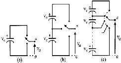
Fig.1 shows a schematic diagram of one-phase leg of inverters with different numbers of levels in which semiconductor is replaced by an ideal switch.Fig.1(a) shows an output voltage of two level with respect to negative terminal of capacitor, while Fig.1(b) shows three level output voltage. Fig.1(c) shows an output voltage of generalized n level. Let p is the number of steps of the phase voltage with respect to the negative terminal of the inverter, then the number of steps in the output voltage between two phases ‘k’ is given by eqn.(1)
k = 2m+1 (1)
————————————————
• Rimpy kalyan is pursuing masters degree program in electrical and electronics engineering in Kurukshetra University, India, PH-
09996831429. E-mail: rimpy.kalyan6@gmail.com
• Co-AuthorNeeraj Bagri is an assistant professor in electrical and electronics department in Doon Valley Institute of Engineering
&Technology, India, E-mail: neerajbagri15@gmail.com
Fig1. Schematic diagram of one phase leg of inverter(a) two-level (b) three- level(c) n-level[1]
In this paper multi-level topology i.e Diode clamped multilevel inverter (three-level DCMLI and five-level DCMLI) is compared with conventional inverter (1800&1200) compared in terms of THD of the output voltage.
Fig.2 shows the single-phase five-level diode clamped multi- level inverter. The main concept of this inverter is to use diodes to limit the voltage stress of power devices [3]. The voltage over each capacitor and each switch is Vdc. An n level inverter needs (n-1) voltage sources, 2(n-1) switching devices and (n-1) (n-2) diodes.[2]
It is basically a type of diode clamped multilevel inverter which gives output as its name suggests in three steps i.e
+Vdc, 0, -Vdc. . In its circuit the dc bus voltage is split into three levels by two series capacitors. It differs from two level inverter in the way that the clamped diodes makes the switch voltage to half the level of the dc bus voltage.
IJSER © 2014 http://www.ijser.org
International Journal of Scientific & Engineering Research, Volume 5, Issue 7, July-2014 1062
ISSN 2229-5518
It is also one of the type of DCMLI in which the dc- bus consists of four capacitors. For dc-bus voltage Vdc, the voltage across each capacitor is Vdc/4 through clamping diodes. There are five switch combinations to synthesize five level voltages which is shown in Table no.2.
In the three phase inverter each SCR conducts for 1800 of a cycle thyristor pair. In each arm ,i.e. S1, S4; S3,S6 and S5, S2 are turned on with the time interval of 1800 it means that S1 conducts for 180o S4 for the next 1800 of a cycle thyristor in the upper group, i.e. S1, S3, S5 conduct at an interval of 1200.It implies that if S1 is fired at wt = to 0o then S3 must be fired at wt = 120oand S5 at wt = 2400. Same is true for lower group SCR’s. We can also use IGBT or any other thyristor in place of SCR.
Table.1. Switching states for various voltages of a phase leg
Voltage level Vao= | S1 | S2 | S3 | S4 |
Vdc/2 | 1 | 1 | 0 | 0 |
-Vdc/2 | 0 | 1 | 1 | 0 |
zero | 0 | 0 | 1 | 1 |
Table.2. Switching states of five level multilevel inverter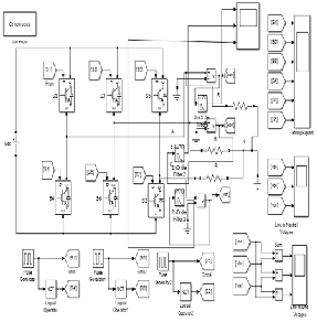
of thyristor S3 and commutation of S1. Hence simulation model for both modes is same . They only differs in the pulse width provided.
Fig.3. Simulation model of three phase 1800 and 1200 mode of conduction
V0 | S1 | S2 | S3 | S4 | S5 | S6 | S7 | S8 |
Vdc/2 | 1 | 1 | 1 | 1 | 0 | 0 | 0 | 0 |
Vdc/4 | 0 | 1 | 1 | 1 | 1 | 0 | 0 | 0 |
0 | 0 | 0 | 1 | 1 | 1 | 1 | 0 | 0 |
-Vdc/4 | 0 | 0 | 0 | 1 | 1 | 1 | 1 | 0 |
-Vdc/2 | 0 | 0 | 0 | 0 | 1 | 1 | 1 | 1 |
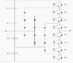
Fig.2. Single phase five-level diode clamped inverter[2]
In this each thyristor conducts for 1200 of a cycle. Like 1800
mode, 1200 mode inverter also requires six steps, each step of
600 duration, for completing one cycle of the output ac voltage. In this inverter too the sequence of firing the six thyristors is same the only difference is that 600 elapses between gating interval of one and commutation interval of second thyristor i.e. S1 conducts for 1200 and 600 elapse occurs between gating
Simulation models of different multilevel inverter topologies are developed in MATLAB/Simulink environment. The parameter used for simulation study are given in Table No.3. Table No.3
DC link parameters
DC link voltage 300V
DC link capacitor 2200 µF
Filter parameter
Cut off freq. 200Hz
Load parameters
Rated line to line voltage 415 V
Load resistance 1 Ω
Frequency 50Hz
Phase voltage Vao and THD analysis of multilevel inverter topologies and conventional inverter are shown in figures . The waveforms of voltages are shown in figures without filtering and with filter.
IJSER © 2014 http://www.ijser.org
International Journal of Scientific & Engineering Research, Volume 5, Issue 7, July-2014 1063
ISSN 2229-5518
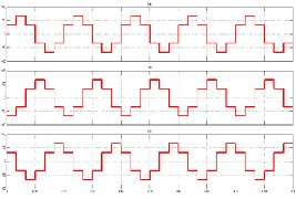
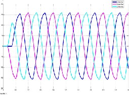
Fig.4. output voltages of conventional inverter (1800)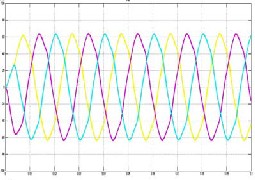
without filter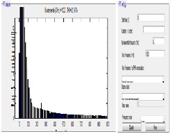
Fig.5. output voltages of conventional (1800) inverter with filter
Fig.6.THD Analysis of conventional (1800) inverter with filter i.e 21.95%
Fig.7. output voltage of conventional inverter (1200) with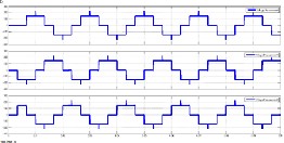
Filter
Fig.9. output voltage of conventional inverter (1200) without filter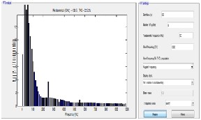
Fig.10. THD of conventional inverter (1200) with filter i.e
22.52%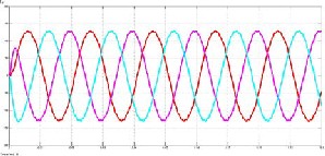
Fig.16. output voltage of three phase five level DCMLI with
Filter
IJSER © 2014 http://www.ijser.org
International Journal of Scientific & Engineering Research, Volume 5, Issue 7, July-2014 1064
ISSN 2229-5518
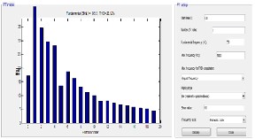
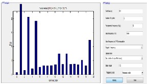
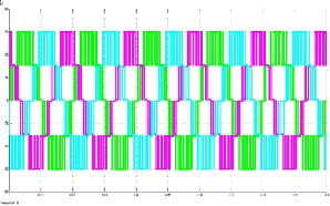 Fig.14. THD of three level DCMLI with filter i.e 20.12%
Fig.17. output voltage of three phase five level DCMLI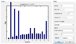
without Filter
Fig.15. THD of three level DCMLI without Filter i.e 39.57%
Fig.18. THD of three phase five level DCMLI with filter i.e
3.68%
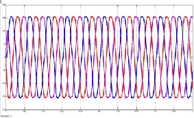
Fig.12.output voltage of three phase three level DCMLI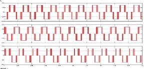
without Filter
Fig.13. output voltage of three phase three level DCMLI
without filter
PWM is a modulation technique that control the width of the rectangular pulse wave resulting in the variation of the average value of the waveform. PWM technique is the intersecting method which require sawtooth or rectangular wave as carrier signal and sinosuidal or rectangular as reference signal as shown in Fig, when the value of reference signal is more than the carrier signal the PWM signal is in high state otherwise it is in low state. The main advantage of PWM technique is that power loss in the switching devices is very low because when the switch is off there is practically no current and when switch is on then voltage drop across the switch is almost zero.
IJSER © 2014 http://www.ijser.org
International Journal of Scientific & Engineering Research, Volume 5, Issue 7, July-2014 1065
ISSN 2229-5518
7. | Three phase five level diode clamped multilevel inverter with filter | 3.68% |
8. | Three phase five level diode clamped multilevel inverter without filter | 34.67% |
In this paper the conventional inverters (1800 and 1200) are studied and analyzed using simulation results in MATLAB/SIMULINK environment. The main focus of the work is to carried out a comparative analysis of conventional inverters with multilevel inverters in terms of THD (Total Harmonic Distortion) of their output voltages. For this comparative analysis different inverters topology are studied and diode clamped multilevel inverter is considered for the comparative analysis. As we know that in case of multilevel inverter the THD of the output voltage decreases with the increase in number of levels. Two types of diode clamped multilevel inverter (three level and five level) are modeled in MATLAB environment. From the various simulation results it is observed that five level multilevel diode clamped inverter is a better choice with THD as compared to other topologies studied in this paper.
[1] J. Rodriguez, J. S. Lai, and F. Z. Peng, “Multilevel inverters: A surveyof topologies, controls, and applications,” IEEE Trans. Ind. Electron., vol. 49, no. 4, pp.
724–738, Aug. 2002
[2] J. S. Lai and F. Z. Peng, “Multilevel converters—A new breed of power converters,” IEEE Trans. Ind. Appl., vol. 32, no. 3, pp. 509–517, May/Jun. 1996 .
[3] L. M. Tolbert, F. Z. Peng, and T. G. Habetler, “Multilevel, converters for large electric drives,” IEEE Trans. Ind. Electron, vol 35, no. 1, pp. 36–44,Jan./Feb. 1999.
[4] M. H. Rashid, Power Electronics Handbook. New York: Academic, 2001, pp. 539–
562.
[5] Sung Geun Song, Feel Soon Kang, Member, IEEE, ,n d Sung-Jun Park, Member
,cascade multilevel inverter using single dc input ,IEEE transactions on industrial electronics, vol. 56, no. 6,june 2009 generation,” IEEE Trans. Ind. Appl., vol. 32, no. 5,
[6] J. N. Chiasson, B. Ozpineci,and L. M. Tolbert, “A five-level three-phase hybrid cascade multilevel inverter using a single DC source for a PM synchronous motor drive,” in Proc. IEEE APEC, 2011,
[7] J. Beristain, J. Bordonau, A. Gilabert, and S. Alepuz, “A new AC/AC multilevel
inverter for a single-phase inverter with HF isolation,” in Proc.IEEE PESC, 2011, vol.3
[8] D. Krug, S. Bernet, S. S. Fazel, K. Jalili, and M. Malinowski,“Comparison of 2.3-kV medium-voltage multilevel inverter for industrial” medium-voltage drives,” IEEE Trans. Ind.Electron., vol. 54, no. 6, pp. 2979–2992, Dec. 2007
[9] P. Lezana, C. A. SilvaY. Sato, M. Kawasaki, and T. Ito Chiba University, Japan “ A Diode-Clamped Multilevel Inverter with Voltage Boost Function” 8th International Conference on Power Electronics - ECCE Asia May 30-June 3, 2011, The Shilla Jeju, Korea
[10] S. Kouro, J. Rebolledo, and J. Rodriguez, “Reduced switching-frequency modulation algorithm for high-power multilevel inverters,” IEEE Trans .Ind. Electron., vol. 54, no.
5, 2894–2901, Oct. 2007
IJSER © 2014 http://www.ijser.org
International Journal of Scientific & Engineering Research, Volume 5, Issue 7, July-2014 1066
ISSN 2229-5518
IJSER © 2014 http://www.ijser.org